
LB1817W
No. 5805-1/9
LB1817W
Package Dimensions
unit: mm
3163A-SQFP48
Any and all SANYO products described or contained herein do not have specifications that can handle
applications that require extremely high levels of reliability, such as life-support systems, aircraft's
control systems, or other applications whose failure can be reasonably expected to result in serious
physical and/or material damage. Consult with your SANYO representative nearest you before using
any SANYO products described or contained herein in such applications.
SANYO assumes no responsibility for equipment failures that result from using products at values that
exceed, even momentarily, rated values (such as maximum ratings, operating condition ranges, or other
parameters) listed in products specifications of any and all SANYO products described or contained
herein.
73099RM(KI)
Ordering number : ENN5805
SANYO Electric Co.,Ltd. Semiconductor Company
TOKYO OFFICE Tokyo Bldg., 1-10, 1 Chome, Ueno, Taito-ku, TOKYO, 110-8534 JAPAN
Monolithic Digital IC
FDD Spindle Motor Driver
[LB1817W]
SANYO : SQFP48
Specifications
Absolute Maximum Ratings
at Ta = 25
�
C
Parameter
Symbol
Conditions
Ratings
Unit
Maximum supply voltage
V
CC
max
7.0
V
Maximum output current
I
CC
max1
t
0.5s
1.5
A
Maximum constant output current
I
O
max2
1.0
A
Allowable power dissipation
Pd max1
IC only
0.45
W
Operating temperature
Topr
�20 to +80
�
C
Storage temperature
Tstg
�40 to +150
�
C
0.5
7.0
9.0
0.15
0.18
0.75
0.5
0.75
0.75
0.5
0.75
0.5
0.1
1
12
13
24
25
36
37
48
7.0
9.0
1.7max
Overview
The LB1817W is a spindle motor driver for low-profile
floppy disk drives.
Functions and Features
� Three-phase full-wave linear drive
(with external PNP transistor)
� Low saturation voltage
� Built-in digital speed control
� Start/stop circuit (Low active)
� Switchable rotation speed
� Current limiter circuit
� Built-in index processing circuit
� Index timing adjustable by VR
� AGC circuit
� Thermal protection circuit
Allowable Operating Ranges
at Ta = 25
�
C
Parameter
Symbol
Conditions
Ratings
Unit
Power supply voltage
V
CC
4.2 to 6.5
V

LB1817W
No. 5805-2/9
Electrical Characteristics
at Ta = 25
�
C, V
CC
= 5V
Parameter
Symbol
Conditions
Ratings
Unit
min
typ
max
Current drain
I
CCO
S/S = 5V (Standby)
70
100
�
A
I
CC
S/S = 0V (Normal)
25
35
mA
MS1 bias current
I
MS
1
V
MS
1 = 5V
180
270
�
A
MS1 Low input voltage
V
MS
1L
0.0
0.8
V
MS1 High input voltage
V
MS
1H
2
V
CC
V
MS2 bias current
I
MS
2
V
MS
2 = 5V
90
135
�
A
MS2 Low input voltage
V
MS
2L
0.0
0.8
V
MS2 High input voltage
V
MS
2H
2
V
CC
V
MS3 bias current
I
MS
3
V
MS
3 = 5V
90
135
�
A
MS3 Low input voltage
V
MS
3L
0.0
0.8
V
MS3 High input voltage
V
MS
3H
2
V
CC
V
S/S bias current
I
S/S
20
�
A
S/S Low voltage
V
S/SL
0.0
0.8
V
S/S High voltage
V
S/SH
2
V
CC
V
Hall amplifier input bias current
I
HB
15
�
A
Common mode input voltage range
Vh
2.0
V
CC
�0.7
V
Differential input voltage range
Vdif
50
200
mVp-p
Input offset voltage
Vho
*
�
10
mV
Hall bias output voltage
V
H
I
H
= 5 mA
0.5
0.8
1.1
V
Leakage current
V
HL
S/S = 5V
�
10
�
A
Output saturation voltage
V(sat)
I
O
= 0.8A
0.45
0.64
V
Output leakage current
I
OL
1
mA
Current limiter
I
lim
R
F
= 3 k
, R
OUT
= 100
6.3
7.5
8.7
mA
Control amplifier voltage gain
G
C
�7.5
�5.5
�3.5
dB
Voltage gain phase differential
G
C
�
1
dB
V/I conversion source current
I
+
19
28
37
�
A
V/I conversion sink current
I
�
�19
�28
�37
�
A
V/I conversion current ratio
I
+
/I
�
0.8
1.0
1.2
DSC buffer input current
I
DSC
1
�
A
FG amplifier input voltage
V
FG
f
FG
= 300 Hz
2
20
mVp-p
FG amplifier voltage gain
G
FG
Open loop*
60
dB
FG amplifier input offset
V
FGO
*
�
10
mV
FG amplifier internal reference voltage
V
FGB
2.2
2.5
2.8
V
FG Schmitt hysteresis width
Vsh1
High �> Low*
25
mV
Vsh2
Low �> High*
25
mV
Speed discriminator count
N
1390/2
Discriminator operating frequency
F
D
*
1.1
MHz
Oscillator frequency
F
OSC
*
1.1
MHz
Oscillator frequency tolerance
F
OSC
�
0.2
%
Index output Low voltage
V
IDL
I
O
= 2 mA
0.4
V
Index output leakage current
I
IDL
�
10
�
A
Index amplifier common mode input voltage range
V
I
0.2
V
CC
�0.7
V
Index amplifier differential input voltage range
V
DIF
Hysteresis width < 25 mA
25
100
mV
Index amplifier hysteresis set current
I
HYS
2.9
4.2
5.5
�
A
Timing adjustment at High level
V
TH
MS1 = L
1.15
1.26
1.35
V
Timing adjustment at Low level
V
TL
MS1 = L
0.40
0.52
0.60
V
Timing adjustment ratio
T
HL
V
TH
(MS1 = L) / V
TH
(MS1 = H)
1.148
Reference voltage
V
REF
1
2.20
2.50
2.80
V
V
REF
2
1.85
2.15
2.45
V
Thermal protection operating temperature
TSD
*
150
180
�
C
Hysteresis width
TSD
*
10
�
C
Note: Items shown to be "*" are not measured.
LB1817W
No. 5805-3/9
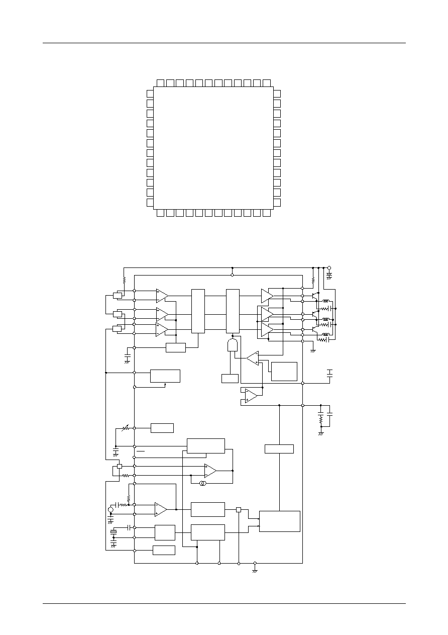
Pin Assignment
Block Diagram
48
1
LB1817W
NC
NC
2
V
REF
1
3
V
REF
2
4
I/D
5
NC
6
SG
7
MS3
8
MS2
9
MS1
10
S/S
11
I
�
12
NC
36
NC
35
UIN1
34
UIN2
33
WPB
32
W
OUT
31
NC
30
VPB
29
V
OUT
28
UPB
27
U
OUT
26
F
G
OUT
25
NC
Top view
47
NC
46
I
+
45
X1
44
X2
43
FC
42
NC
41
Rf
40
PG
39
FG
+
38
FG�
37
13
14
15
16
17
18
19
20
21
22
23
24
NC
NC
NC
CT
DSC
AGC
V
CC
HB
WIN1
WIN2
VIN1
VIN2
NC
PGND
W
OUT
V
OUT
U
OUT
W
PB
V
PB
U
PB
R
F
LB1817W
V
CC
V
CC
U
IN
1
U
IN
2
V
CC
FC
DSC
V
IN
1
V
IN
2
W
IN
1
W
IN
2
AGC
HB
S/S
V
REF
1
V
U
W
W
I+
CT
5
�
A
FG OUT
750k
12k
0.22
�
F
I/D
I�
FG�
FG+
X2
X1
SGND
MS3
MS2
(1:2)
H:2
L:1
MS1
(1:1.2)
H:1.2
L:1
H:360rpm
L:300rpm
1MHz
V
REF
2
V
U
HU
HV
HW
AGC
TSD
V
REF
1
V
REF
2
Timing
adjustment
Schmitt
comparator
1 / N
OSC
V/I
Hall amplifier
Matrix
Current control
Output amplifier
Control
amplifier
Hall bias
Current
limiter
V
LIM
Buffer amplifier
FG amplifier
Speed
discriminator
(1390/2 count)
N
(
)

LB1817W
No. 5805-4/9
Pin number
1,
5
12, 13
14, 19
24, 25
31, 36
37, 47
48
2
3
4
6
7
8
Pin name
NC
V
REF
1
V
REF
2
I/D
SG
MS3
MS2
Equivalent circuit
Pin Descriptions
Pin function
� Pins not used
� V
REF
1 pin.
Used as power supply for external CR
serving for index timing adjustment.
� V
REF
2 pin.
Used as bias pin for external index
sensor.
� Index pulse output pin.
� Signal ground pin.
Connect to ground together with pin 21.
� FG switching pin.
High: FG set to through
Low: FG set to 1-stage division
� CLK switching pin.
High: Clock set to through
Low: Clock set to 1-stage division
Pin voltage
2.5V typ
2.15V typ
H: 2.0V min
L: 0.8V max
H: 2.0V min
L: 0.8V max
100
V
CC
2
V
CC
4
V
CC
50k
50k
7
Continued on next page
V
CC
3
V
CC
50k
50k
8

LB1817W
No. 5805-5/9
Continued from preceding page
Pin number
9
10
11
15
16
17
18
Pin name
MS1
S/S
I
�
I
+
X1
X2
FC
Equivalent circuit
Pin function
� Rotation speed switching pin.
High: 360 rpm
Low: 300 rpm
For details, see rotation speed switching
table.
� Start/stop switching pin.
Low: active
� External index � input pin.
� External index + input pin.
When I
�
pin is High, constant current I1
flows. When pin is Low, constant current
I1 is cut off.
Resistor externally connected to I
�
pin
determines hysteresis width.
� Reference clock generator pin.
� Frequency characteristics compensation
pin.
To prevent current control loop oscillation,
insert a capacitor between this pin and
V
CC
.
Pin voltage
H: 2.0V min
L: 0.8V max
H: 2.0V min
L: 0.8V max
Continued on next page
V
CC
50k
50k
9
50k
50k
V
CC
10
200
V
CC
200
200
I1
11
15
V
CC
200
17
18
V
CC
400
200
200
16