Ordering number : EN4881A
N2095HA (OT)/11895TH (OT)No. 4881-1/16
Overview
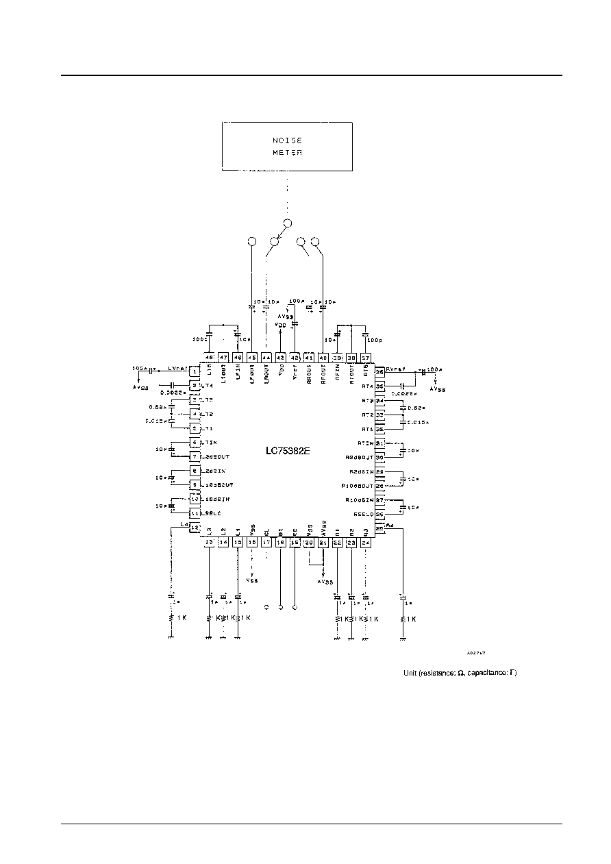
The LC75382E is an electronic tone control IC that can
implement, with minimal external components, the
complete range of tone and volume controls required in a
car stereo, including volume, balance, fader, bass and
treble, input switching and input level controls.
Features
∑ Volume:
Controls the left and right volume levels
independently from 0 dB to ≠78 dB (in
2 dB steps) and ≠
dB (41 settings).
Since the left and right levels are
independent this circuit also functions as
a balance control.
∑ Fader:
Attenuates either the rear or front outputs
over 16 levels, from 0 dB to ≠20 dB in
2 dB steps, from ≠20 dB to ≠25 dB in
5 dB step, from ≠25 dB to ≠45 dB in
10 dB steps and then to ≠60 dB and ≠
dB.
∑ Bass/treble:
Implements 21 position bass and treble
controls with the addition of external
capacitors.
∑ Input selector: Selects one of four inputs for both the
left and right channels. The selected
input signal can be amplified by between
0 dB and +18 dB in 6 dB steps.
∑ The provision of on-chip operational amplifiers means
that few external components are required.
∑ Fabricated in a silicon gate process for minimal
switching noise.
∑ All functions can be controlled by serial data over a
CCB interface.
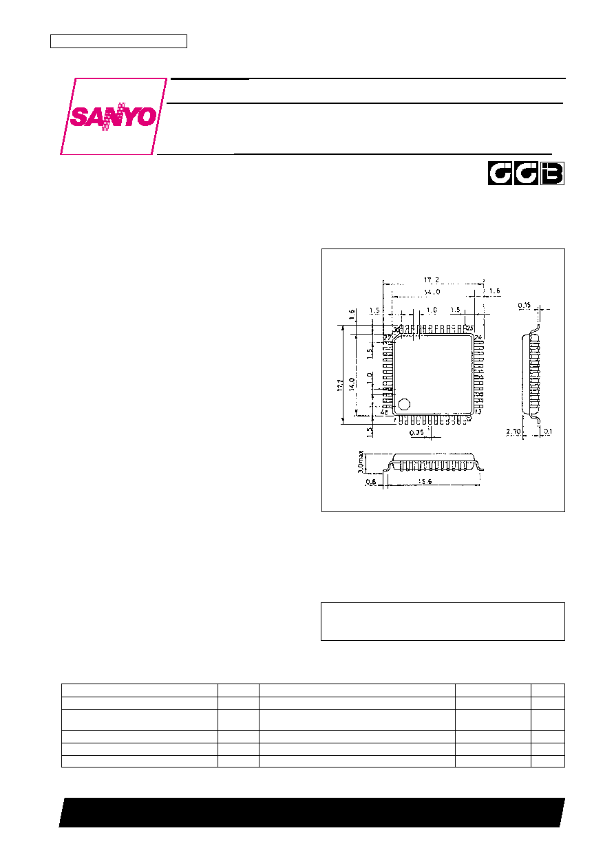
Package Dimensions
unit: mm
3156-QFP48E
SANYO: QIP48E
[LC75382E]
LC75382E
SANYO Electric Co.,Ltd. Semiconductor Bussiness Headquarters
TOKYO OFFICE Tokyo Bldg., 1-10, 1 Chome, Ueno, Taito-ku, TOKYO, 110-8534 JAPAN
Electronic Tone Controls
for Car Stereo Systems
CMOS LSI
∑ CCB is a trademark of SANYO ELECTRIC CO., LTD.
∑ CCB is SANYO's original bus format and all the bus
addresses are controlled by SANYO.
Specifications
Absolute Maximum Ratings
at Ta = 25∞C, V
SS
= 0 V
Parameter
Symbol
Conditions
Ratings
Unit
Maximum supply voltage
V
DD
max
V
DD
12
V
Maximum input voltage
V
IN
max
CL, DI, CE, LTIN, RTIN, L10dBIN, R10dBIN, L2dBIN,
V
SS
≠ 0.3 to
V
R2dBIN, LFIN, RFIN, L1 to L4, R1 to R4
V
DD
+ 0.3
Allowable power dissipation
Pd max
Ta
85∞C
310
mW
Operating temperature
Topr
≠40 to +85
∞C
Storage temperature
Tstg
≠50 to +125
∞C

Allowable Operating Ranges
at Ta = 25∞C, V
SS
= 0 V
Electrical Characteristics
at Ta = 25∞C, V
DD
= 9 V, V
SS
= 0 V
No. 4881-2/16
LC75382E
Parameter
Symbol
Conditions
min
typ
max
Unit
Supply voltage
V
DD
V
DD
6.0
11.0
V
Input high level voltage
V
IH
CL, DI, CE
4.0
V
DD
V
Input low level voltage
V
IL
CL, DI, CE
V
SS
1.0
V
Input voltage amplitude
V
IN
LTIN, RTIN, L10dBIN, R10dBIN, L2dBIN, R2dBIN,
V
SS
V
DD
Vp-p
LFIN, RFIN, L1 to L4, R1 to R4
Input pulse width
t
¯W
CL
1
µs
Setup time
t
setup
CL, DI, CE
1
µs
Hold time
t
hold
CL, DI, CE
1
µs
Operating frequency
fopg
CL
500
kHz
Parameter
Symbol
Conditions
min
typ
max
Unit
[Input Block]
Input resistance
Rin
L1 to L4, R1 to R4
1
M
Clipping level
Vcl
LSELO, RSELO: THD = 1.0%
2.35
Vrms
Output load resistance
R
L
LSELO, RSELO
10
k
Minimum input gain
Gin min
≠2
0
+2
dB
Maximum input gain
Gin max
+16.0
+18.0
+20.0
dB
Step resolution
Gstep
+6.0
dB
[Volume Block]
Input resistance
Rv10
L10dBIN, R10dBIN: 10 dB steps
21
35
49
k
Rv2
L2dBIN, R2dBIN: 2 dB steps
6
10
14
k
Step resolution
ATstep
2
dB
Step error
ATerr
step = 0 to ≠40 dB
≠2
0
+2
dB
[Fader Volume Block]
Input resistance
Rfed
LFIN, RFIN
12
20
28
k
step = 0 to ≠20 dB
2
dB
Step resolution
ATstep
step = ≠20 to ≠25 dB
5
dB
step = ≠25 to ≠45 dB
10
dB
Step error
ATerr
step = 0 to ≠40 dB, step = ≠40 to ≠60 dB
≠2
0
+2
dB
Output load resistance
R
L
LFOUT, LROUT, RFOUT, RROUT
10
k
[Bass/Treble Control Block]
Control range
Gbass, Gtre Max. Boost/Cut
±15
±17
±19
dB
Step resolution
Bstep
0.7
1.7
2.7
dB
Internal feedback resistance
Rfeed
46
76
107
k
[Overall Characteristics]
Total harmonic distortion
THD (1)
V
IN
= 300 mVrms, f = 1 kHz, all controls flat overall
0.005
0.01
%
THD (2)
V
IN
= 300 mVrms, f = 20 kHz, all controls flat overall
0.008
0.02
%
Crosstalk
CT
V
IN
= 1 Vrms, f = 1 kHz, all controls flat overall,
60
84.5
dB
Rg = 1 k
Output at maximum attenuation
V
O
min
V
IN
= 1 Vrms, f = 1 kHz, Main volume at ≠
≠65
≠74.5
dB
V
N
(1)
All controls flat overall (IHF-A), Rg = 1 k
5.2
12
µV
V
N
(2)
All controls flat overall (DIN-AUDIO), Rg = 1 k
7.2
16
µV
Output noise voltage
V
N
(3)
All controls flat overall (NO-FILTER), Rg = 1 k
9.2
20
µV
V
N
(4)
Gv = +18dB (IHF-A), Rg = 1 k
23
50
µV
V
N
(5)
Bass at maximum boost, treble at maximum boost
48
120
µV
(IHF-A), Rg = 1 k
Current drain
I
DD
V
DD
≠ V
SS
= 11 V
28
33
mA
Input high level current
I
IH
CL, DI, CE: V
IN
= 9 V
10
µA
Input low level current
I
IL
CL, DI, CE: V
IN
= 0 V
≠10
µA