 | –≠–ª–µ–∫—Ç—Ä–æ–Ω–Ω—ã–π –∫–æ–º–ø–æ–Ω–µ–Ω—Ç: LC78835 | –°–∫–∞—á–∞—Ç—å:  PDF PDF  ZIP ZIP |

Overview
The LC78835K and 78835KM are 18-bit digital-to-analog
D/A converter CMOS ICs with an on-chip eight-times
oversampling digital filter. The LC78835 and the
LC78835M are pin compatible.
Features
∑ Digital filter
-- 8 fs oversampling filter: 3-stage finite-impulse-
response (FIR) filter design (43rd-, 11th-, and third-
orders)
-- De-emphasis filter: Supports fs = 32 kHz, 44.1 kHz,
or 48 kHz
-- Soft mute
-- Noise shaper
-- Supports double-rate sampling
∑ D/A converter
-- Dynamic level-shifting 18-bit digital-to-analog
converter
-- On-chip 2-channel D/A converter (with
corresponding output)
-- On-chip output op-amp
-- Supports 384 fs, 392 fs, 448 fs, or 512 fs system
clock
-- Single 5 V supply
-- Permits low-voltage operation (3.5 V)
-- Low-power silicon-gate CMOS process
Package Dimensions
unit: mm
3092-DIP24W
unit: mm
3155-MFP24
CMOS IC
Ordering number : EN4624B
73696HA (OT)/N1094TH (OT)/82793JN No. 4624-1/14
SANYO: DIP24W
[LC78835K]
SANYO: MFP24
[LC78835KM]
SANYO Electric Co.,Ltd. Semiconductor Bussiness Headquarters
TOKYO OFFICE Tokyo Bldg., 1-10, 1 Chome, Ueno, Taito-ku, TOKYO, 110 JAPAN
18 Bits Digital Filter and D/A Converter
for Digital Audio
LC78835K, 78835KM
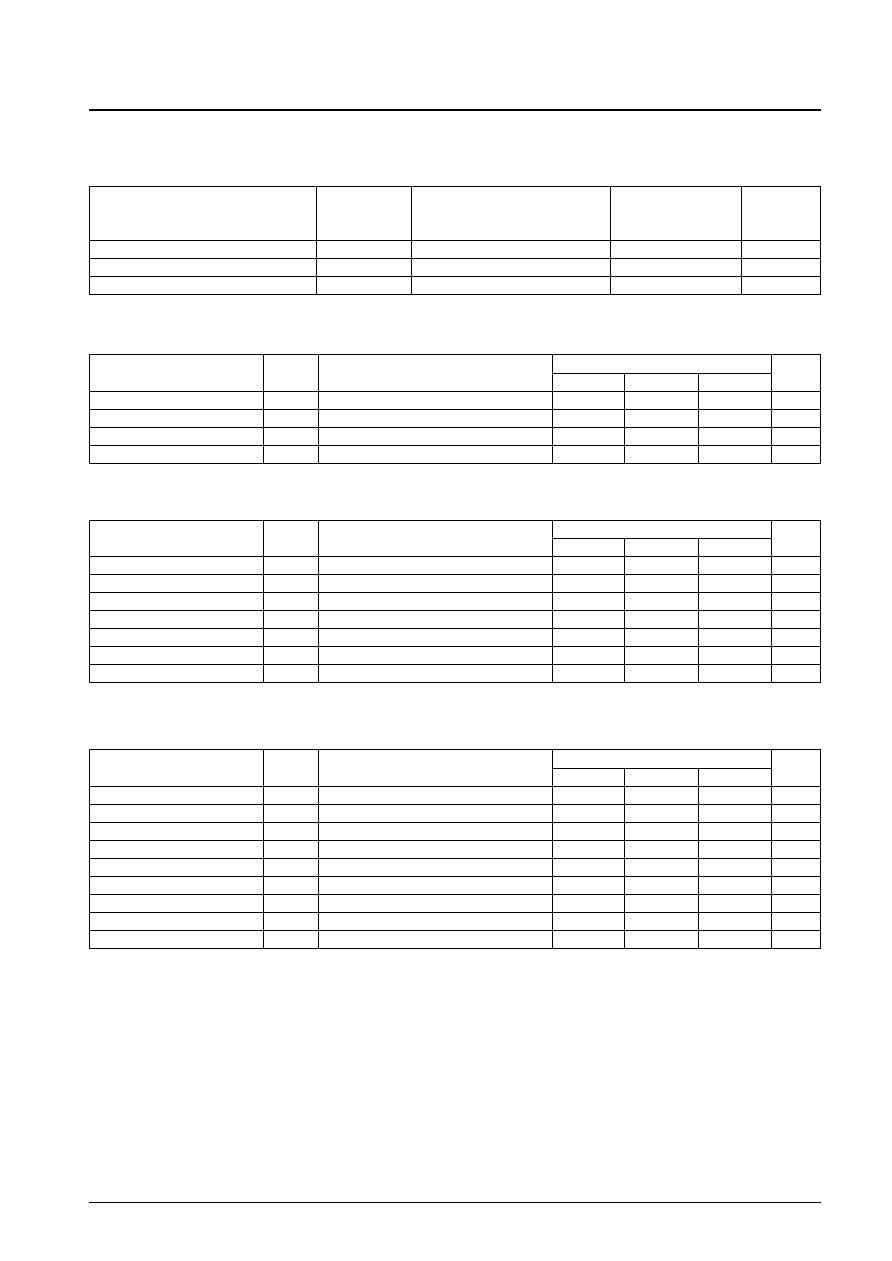
Specifications
Absolute Maximum Ratings
at Ta = 25∞C, V
SS
= 0∞C
Allowable Operating Ranges
DC Characteristics
at Ta = ≠30 to +75∞C, V
DD
= 3.5 to 5.5 V, V
SS
= 0 V
Note:
*
3, 4, 5, 6, 7, 11, 13, 14, 15, 16, 17 and 18 pin
AC Characteristics
at Ta = ≠30 to +75∞C, V
DD
= 3.5 to 5.5 V, V
SS
= 0 V
No. 4624-2/14
LC78835K, 78835KM
Parameter
Symbol
Conditions
Ratings
Unit
Maximum supply voltage
V
DD
max
≠0.3 to + 7.0
V
Input voltage
V
IN
≠0.3 to V
DD
+ 0.3
V
Output voltage
V
OUT
≠0.3 to V
DD
+ 0.3
V
Operating temperature
Topr
≠30 to + 75
∞C
Storage temperature
Tstg
≠40 to + 125
∞C
Parameter
Symbol
Conditions
Ratings
Unit
min
typ
max
Supply voltage
V
DD
3.5
5.0
5.5
V
Reference voltage high
Vref H
V
DD
≠ 0.3
V
DD
V
Reference voltage low
Vref L
0
0.3
V
Operating temperature
Topr
≠30
+75
∞C
Parameter
Symbol
Conditions
Ratings
Unit
min
typ
max
Input high level voltage (1)
V
IH
1
3, 4, 5, 6, 7, 13, 14, 15, 16, 17 and 18 pin
2.2
V
Input low level voltage (1)
V
IL
1
3, 4, 5, 6, 7, 13, 14, 15, 16, 17 and 18 pin
0.8
V
Input high level voltage (2)
V
IH
2
11 pin
0.7V
DD
V
Input low level voltage (2)
V
IL
2
11 pin
0.3V
DD
V
Output high level voltage
V
OH
9 pin: I
OH
= ≠3 mA
2.4
V
Output low level voltage
V
OL
9 pin: I
OL
= 3 mA
0.4
V
Input leakage current
I
L
*
, V
I
= V
SS
, V
DD
≠25
+25
µA
Parameter
Symbol
Conditions
Ratings
Unit
min
typ
max
Oscillation frequency
f
X
XIN pin for crystal oscillator
1.0
25
MHz
Clock pulse width
t
CW
With external clock input to other than XIN pin
18
ns
Clock pulse phase
t
CY
With external clock input to other than XIN pin
40
1000
ns
BCLK pulse width
t
BCW
60
ns
BCLK pulse phase
t
BCY
120
ns
Data setup time
t
DS
40
ns
Data hold time
t
DH
40
ns
LRCK setup time
t
LRS
40
ns
LRCK hold time
t
LRH
40
ns

Audio Input Waveforms
Electrical Characteristics (1)
at Ta = 25∞C, AV
DD
= DV
DD
= V
refH
= 5.0 V, AGND = DGND = V
refL
= 0 V, unless otherwise specified
Note: 1. "0 dB" signifies full scale.
2. XIN pulse width (pin 11) 1.5 to 3.5 V, fx = 16.9344 MHz
Test circuit: Based on application circuit
No. 4624-3/14
LC78835K, 78835KM
Parameter
Symbol
Conditions
Ratings
Unit
min
typ
max
D/A converter resolution
RES
18
Bits
Total harmonic distortion
THD
At 1 kHz, 0 dB
*
1
0.08
%
Dynamic range
DR
At 1 kHz, ≠60 dB
90
dB
Crosstalk
CT
At 1 kHz, 0 dB
≠85
dB
Signal-to-noise ratio
S/N
JIS-A
96
dB
Full-scale output voltage
VFS
3.0
V
P-P
Power dissipation
Pd
*
2
135
200
mW
Output load resistance
RL
21, 23 pin
5
k

Electrical Characteristics (2)
at Ta = 25∞C, AV
DD
= DV
DD
= VrefH 3.5 V, AGND = DGND = VrefH = 0 V, unless otherwise specified
Note: 1. "0 dB" signifies full scale.
2. XIN pulse width (pin 11) 1.0 to 2.5 V, fx = 16.9344 MHz
Test circuit: Based on application circuit
Block Diagram
Pin Assignment
No. 4624-4/14
LC78835K, 78835KM
Parameter
Symbol
Conditions
Ratings
Unit
min
typ
max
D/A converter resolution
RES
18
Bits
Total harmonic distortion
THD
At 1 kHz, 0dB
*
1
0.09
%
Dynamic range
DR
At 1 kHz, ≠60 dB
90
dB
Crosstalk
CT
At 1 kHz, 0 dB
≠85
dB
Signal-to-noise ratio
S/N
JIS-A
96
dB
Full-scale output voltage
VFS
2.1
V
P-P
Power dissipation
Pd
*
2
50
75
mW
Output load resistance
RL
21, 23 pin
15
k

Pin Description
No. 4624-5/14
LC78835K, 78835KM
Number
Name
Description
1
REFH
Reference voltage "H" pin
Normally connected to AGND via a capacitor
2
VrefH
Reference voltage "H" input pin
3
MUTE
Mute signal input pin
Soft mute is on when high
4
D/N
Normal/double-speed operation toggle
Double-speed operation when high, normal operation when low
5
BCLK
Bit clock input pin
6
DATA
Digital audio data input pin
2's complement code, with input from the most significant bit (MSB)
7
LRCK
Left-right clock input pin
Channel 1 when high, channel 2 when low
8
DV
DD
Digital power supply pin
9
CKOUT
Clock output pin
When at 392 fs: 196 fs clock
When not at 392 fs: XIN-frequency clock
10
XOUT
Crystal oscillator output pin (system clock output pin)
11
XIN
Crystal oscillator input pin (system clock input pin)
12
DGND
Digital ground pin
13
INITB
Initialization signal input pin
Initialization performed when low
14
EMP
On/Off toggle for the de-emphasis filter
On when high, off when low
15
FS1
32 kHz/44.1 kHz/48 kHz selector for the de-emphasis filter
16
FS2
17
CKSL1
System clock selector pin
18
CKSL2
19
VrefL
Reference voltage "L" input pin
20
REFL
Reference voltage "L" pin
Normally connected to AGND via a capacitor
21
CH2OUT
Channel 2 analog output pin
22
AGND
Analog ground pin
23
CH1OUT
Channel 1 analog output pin
24
AV
DD
Analog power supply pin
FS1
L
H
H
L
FS2
L
L
H
H
fs
44.1 kHz
32 kHz 48 kHz
CKSL1
CKSL2
System Clock
L
L
384 fs
L
H
392 fs
H
L
448 fs
H
H
512 fs