 | –≠–ª–µ–∫—Ç—Ä–æ–Ω–Ω—ã–π –∫–æ–º–ø–æ–Ω–µ–Ω—Ç: LC99452 | –°–∫–∞—á–∞—Ç—å:  PDF PDF  ZIP ZIP |
Ordering number : ENN
*
6298
N2599RM(OT) No. 6298-1/5
Features
∑ Very high resolution: 1616
◊
1296 (H
◊
V) pixels.
progressive scan
∑ 2/3 inch image area: 8.24mm
◊
6.61mm. Image diagonal
10.56mm
∑ Square pixel: 5.1µm
◊
5.1µm
∑ Color filter: R-G-B primary mosaic filter
∑ High sensitivity
∑ High dynamic range
∑ Low dark current
∑ Low noise
∑ Fast readout: 25 MHz horizontal drive frequency.
5 full-resolution images/s
∑ Electronic shuttering
∑ Supports monitoring modes
∑ Compact package: 20-pin leadless ceramic chip-carrier
(LCC)
Device Structure
∑ General
Frame-Transfer CCD with reduced storage section
Chip size: 9.49 mm (H)
◊
9.32 mm (V)
Package dimension
∑ Image Area
Unit cell size: 5.1 µm (H)
◊
5.1 µm (V)
Number of effective pixels: 1616 (H)
◊
1296 (V)
approx. 2094 k pixels.
Optical black: 12/Top + 12/Bottom 2/Left + 70/Right
Number of dummy lines: 4 /Bottom
Total number of pixels: 1688 (H)
◊
1324 (V)
approx. 2235k pix.
Effective Image size: 8.24 mm (H)
◊
6.61 mm (V)
Image diagonal: 10.56 mm (2/3 inch format)
Aspect ratio: 5:4 (or 4:3)
Color filter pattern: R-G-B; Bayer
Number of clock phase: 4
∑ Storage Area
Unit cell size: 5.1 µm (H)
◊
5.1 µm (V)
Number of cells: 1688 (H)
◊
298 (V)
Number of clock phase: 4
∑ Horizontal Register and Output Stage
Number of cells: 1696 (H)
◊
1 (V)
Number of dummy cells: 8/Front
Number of clock phase: 4
Output Stage: 3-stage source follower (open source)
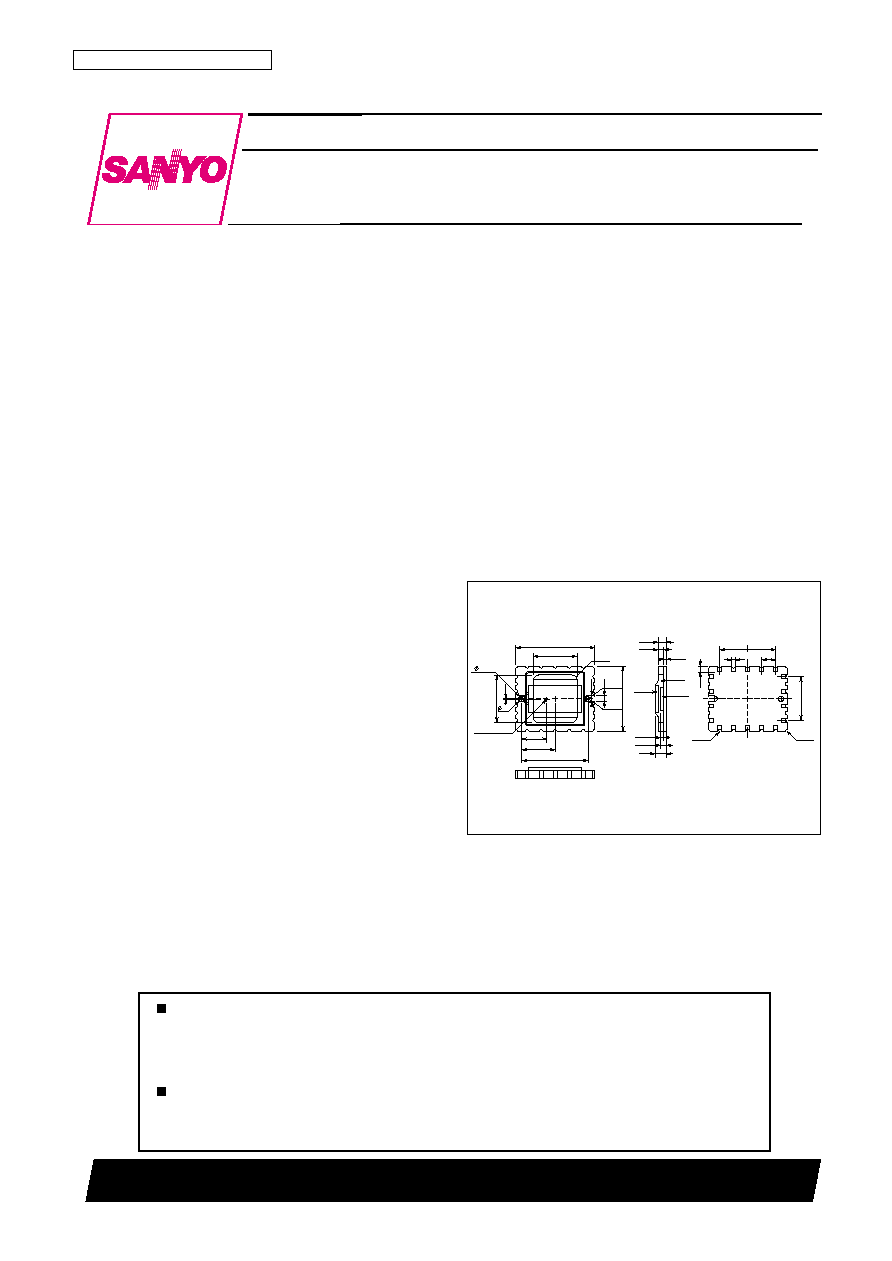
Package Dimensions
unit: mm
3258
Preliminary
LC99452
SANYO Electric Co.,Ltd. Semiconductor Company
TOKYO OFFICE Tokyo Bldg., 1-10, 1 Chome, Ueno, Taito-ku, TOKYO, 110-8534 JAPAN
2M pixel 2/3-inch Progressive Scan
CCD Image Sensor with Square Pixel
Any and all SANYO products described or contained herein do not have specifications that can handle
applications that require extremely high levels of reliability, such as life-support systems, aircraft's
control systems, or other applications whose failure can be reasonably expected to result in serious
physical and/or material damage. Consult with your SANYO representative nearest you before using
any SANYO products described or contained herein in such applications.
SANYO assumes no responsibility for equipment failures that result from using products at values that
exceed, even momentarily, rated values (such as maximum ratings, operating condition ranges, or other
parameters) listed in products specifications of any and all SANYO products described or contained
herein.
1.49
1.05
0.44
0.635
1.075
2.0
Resin
Glass
Sensor
1.015
10.16
0.7
2.54
1.0
7.62
R0.3
R0.25
4.65
6.0
12.3
11.8
14.3
8.0
R1.0
8.6
0.15
1.0
(1.2)
(R0.6)
(R0.5)
1.2
Optical Center
[LC99452]
No. 6298-2/5
LC99452
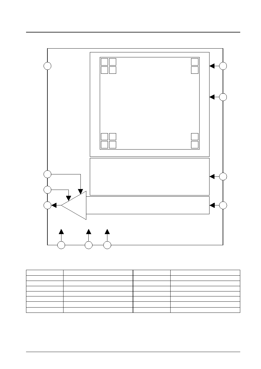
Block Diagram and Pixel Arrangement
G
B
R
G
G
B
R
G
B
G
B
G
Vout
Phi-R
N-SUB
VPW
Phi
1 to 4
Phi-S
1 to 4
Phi-H
1 to 4
Phi-R
Vrd
Vog
Vss
Vdd
A12757
Image area
Optical Black Area
Storage Area
Horizontal Shift Register
Output Amplifier
Pin Function
Symbol
Description
Symbol
Description
N-sub
N-Substrate
Phi 1 to 4
Image area clock
Vpw
P-Well
Phi-S 1 to 4
Storage area clock
Vdd
Power supply
Phi-H 1 to 4
Horizontal register clock
Vss
Power supply Source
Phi-R
Reset gate
Vog
CCD output gate
Vrd
Reset drain
Vout
CCD output
No. 6298-3/5
LC99452
Modes of Operation
The LC99452 has been especially designed for high-resolution low cost digital photography in color full 1600
◊
1280
resolution and real-time monitoring (preview) mode in color at reduced resolution. Two main modes of operation are
possible:
Still picture mode (mode-1)
In still picture mode, a 1600 (H)
◊
1280 (V) progressive scan image can be read out. A 'single shot' mechanical shutter is
required to obtain a 100% smear free image.
Preview mode (mode-2)
In preview mode, image with a reduced vertical resolution by on-chip data compression can be obtained. Progressive
scan images (mode-2), e.g. 120, 240 or 288 lines at up to 40 images/s, suitable for LCD displays can be selected by the
timing generator.
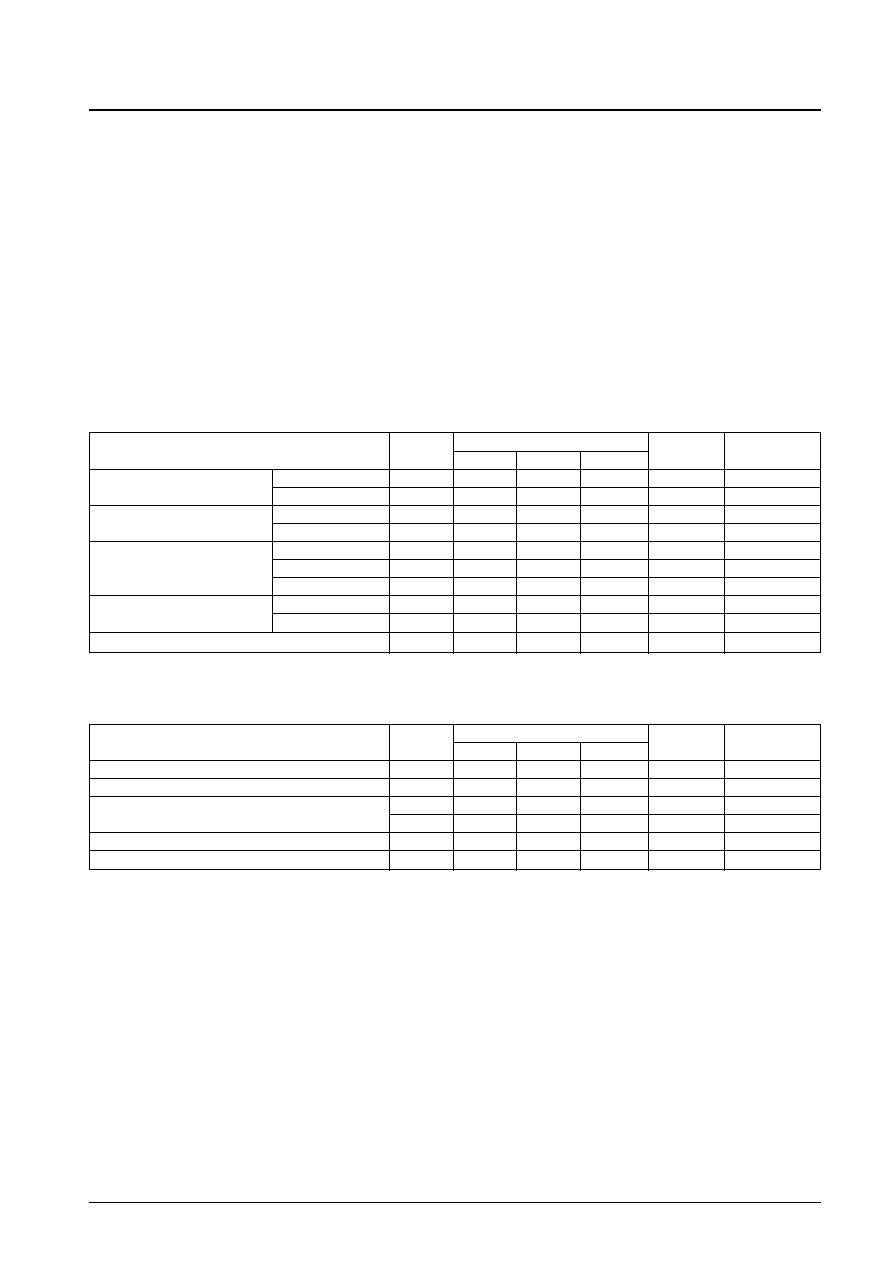
Clock Voltage Conditions
Parameter
Symbol
Ratings
Unit
Cap per phase
min
typ
max
Input resistanImage area pulses
Pulse amplitude
V
PIF
11
12
13
V
5.5 nF
Phi 1 to 4
Low level
V
LIF
0
V
Storage area pulses
Pulse amplitude
V
PSL
11
12
13
V
1.5 nF
Phi-S 1 to 4
Low level
V
LSL
0
V
Horizontal register pulses
Pulse amplitude
V
PH
4.5
5.0
5.25
V
60 pF
Phi-H 1 to 4
Low level C1,C3
V
LH 13
0
V
Low level C2,C4
V
LH 24
2.5
3
3.5
V
Reset gate pulses
Pulse amplitude
V
PR
4.5
5
5.25
V
15 pF
*
1
Phi-R
High level
V
HR
21
22
23
V
Charge reset pulse on Nsub
V
PSUB
4.5
5
5.5
V
Note:
*
1. DC setting depends on RG clock-swing.
DC Electrical Characteristics
Parameter
Symbol
Ratings
Unit
I (mA)
min
typ
max
N-sub bias
V
LSUB
20
24
28
V
2
*
1
P-well bias
V
PW
6
7
9
V
2
Output circuit power supply
V
DD
19
20
21
V
5.5
*
2
V
SS
0
0
0
V
1
*
2
OG bias
V
OG
3.5
4.0
4.5
V
*
3
Reset drain bias
V
RD
19
20
21
V
Notes: 1. V
LSUB
is set for optimal anti-blooming operation.
2. with RL = 3.3 k
, V
DD
should be adjusted at the same voltage as V
RD
.
3. OG setting depends on horizontal clock amplitude.
No. 6298-4/5
LC99452
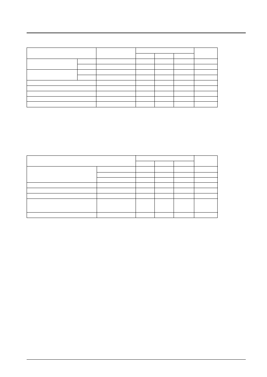
AC Electrical Characteristics
Parameter
Conditions
Ratings
Unit
min
typ
max
Transport frequency:
- horizontal
25
MHz
- vertical
1.56
*
1
3.125
MHz
Power consumption
mode 1
mW
mode 2
mW
Output impedance
400
Amplifier supply current
(R
L
= 3.3 k
)
5.2
mA
Bandwidth (R
L
= 3.3 k
, C
L
= 2pF)
90
MHz
RMS readout noise
@ 5 MHz BW (after CDS)
0.240
0.330
mV
Power supply rejection ratio at DC
*
2
0.15
0.2
V/V
Notes: 1. Typical value for preview and movie mode.
2. V
DD
must be decoupled properly with a 100 nF decoupling capacitor close to the pin.
Performance Characteristics
Test conditions: Typical conditions
Image capture mode (mode-1) of operation
Integration time = 1/30 sec.( unless specified differently )
Test temperature 60∞C; light source 3200 K; IR filter 1.7 mm BG40; F = 16
Parameter
Ratings
Unit
min
typ
max
green pixels
295
mV / lux
∑
s
Sensitivity
red pixels
240
mV / lux
∑
s
blue pixels
175
mV / lux
∑
s
Saturation signal
840
1150
1320
mV / lux
∑
s
Qmax
40
50
60
k-electrons
Blooming suppression
100
x Qmax
Dark conditions:
Average number of dark signal electrons
25
electrons
per pixel after 1/30 sec integration
Dark signal shading
1
mV
PS No. 6298-5/5
LC99452
This catalog provides information as of November, 1999. Specifications and information herein are
subject to change without notice.
Specifications of any and all SANYO products described or contained herein stipulate the performance,
characteristics, and functions of the described products in the independent state, and are not guarantees
of the performance, characteristics, and functions of the described products as mounted in the customer's
products or equipment. To verify symptoms and states that cannot be evaluated in an independent device,
the customer should always evaluate and test devices mounted in the customer's products or equipment.
SANYO Electric Co., Ltd. strives to supply high-quality high-reliability products. However, any and all
semiconductor products fail with some probability. It is possible that these probabilistic failures could
give rise to accidents or events that could endanger human lives, that could give rise to smoke or fire,
or that could cause damage to other property. When designing equipment, adopt safety measures so
that these kinds of accidents or events cannot occur. Such measures include but are not limited to protective
circuits and error prevention circuits for safe design, redundant design, and structural design.
In the event that any or all SANYO products (including technical data, services) described or contained
herein are controlled under any of applicable local export control laws and regulations, such products must
not be exported without obtaining the export license from the authorities concerned in accordance with the
above law.
No part of this publication may be reproduced or transmitted in any form or by any means, electronic or
mechanical, including photocopying and recording, or any information storage or retrieval system,
or otherwise, without the prior written permission of SANYO Electric Co., Ltd.
Any and all information described or contained herein are subject to change without notice due to
product/technology improvement, etc. When designing equipment, refer to the "Delivery Specification"
for the SANYO product that you intend to use.
Information (including circuit diagrams and circuit parameters) herein is for example only; it is not
guaranteed for volume production. SANYO believes information herein is accurate and reliable, but
no guarantees are made or implied regarding its use or any infringements of intellectual property rights
or other rights of third parties.