Absolute Maximum Ratings
( T
J
= 25∞C unless otherwise specified )
Symbol
Parameter
Condition
Ratings
Units
V
DRM
Repetitive Peak Off-State Voltage
600
V
I
T(AV)
Average On-State Current
Half Sine Wave : T
C
= 106 ∞C
3.8
A
I
T(RMS)
R.M.S On-State Current
180∞ Conduction Angle
6
A
I
TSM
Surge On-State Current
1/2 Cycle, 60Hz, Sine Wave
Non-Repetitive
66
A
I
2
t
I
2
t
for Fusing
t = 8.3ms
21
A
2
s
di/dt
Critical rate of rise of on-state current
50
A/
P
GM
Forward Peak Gate Power Dissipation
5
W
P
G(AV)
Forward Average Gate Power Dissipation
0.5
W
I
FGM
Forward Peak Gate Current
2
A
V
RGM
Reverse Peak Gate Voltage
5.0
V
T
J
Operating Junction Temperature
- 40 ~ 125
∞C
T
STG
Storage Temperature
- 40 ~ 150
∞C
SCR6C60
Dec, 2002. Rev. 3
Features
Repetitive Peak Off-State Voltage : 600V
R.M.S On-State Current ( I
T(RMS)
= 6 A )
Low On-State Voltage (1.4V(Typ.)@ I
TM
)
General Description
Standard gate triggering SCR is suitable for the application where
requiring high bidirectional blocking voltage capability and also
suitable for over voltage protection ,motor control circuit in power
tool, inrush current limit circuit and heating control system.
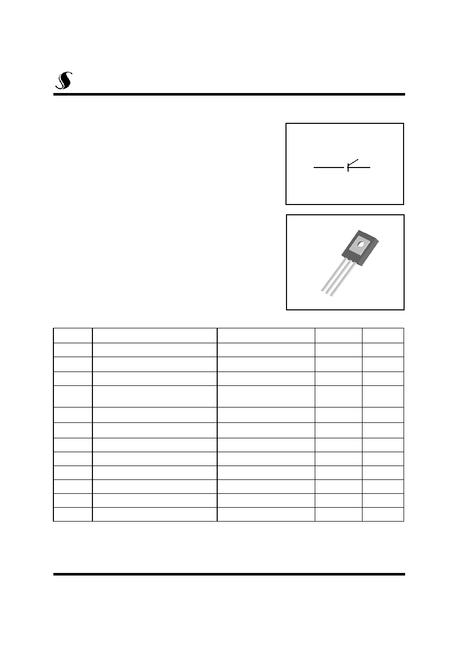
3. Gate
1. Cathode
Symbol
1/5
SemiWell
Semiconductor
Silicon Controlled Rectifiers
2. Anode
3
2
1
Copyright@SemiWell Semiconductor Co., Ltd., All rights are reserved.
TO-126

Electrical Characteristics
( T
C
= 25 ∞C unless otherwise noted )
Symbol
Items
Conditions
Ratings
Unit
Min.
Typ.
Max.
I
DRM
Repetitive Peak Off-State
Current
V
AK
= V
DRM
T
C
= 25 ∞C
T
C
= 125 ∞C
10
200
V
TM
Peak On-State Voltage (1)
I
TM
= 9 A tp=380
1.6
V
I
GT
Gate Trigger Current (2)
V
AK
= 6 V(DC), R
L
=10
T
C
= 25 ∞C
15
mA
V
GT
Gate Trigger Voltage (2)
V
D
= 6 V(DC), R
L
=10
T
C
= 25 ∞C
1.5
V
V
GD
Non-Trigger Gate Voltage (1)
V
AK
= 12 V, R
L
=100
T
C
= 125 ∞C
0.2
V
dv/dt
Critical Rate of Rise Off-State
Voltage
Linear slope up to V
D
= V
DRM
67%
,
Gate open T
J
= 125∞C
200
V/
I
H
Holding Current
I
T
= 100mA, Gate Open
T
C
= 25 ∞C
20
mA
R
th(j-c)
Thermal Impedance
Junction to case
3.12
∞C/W
R
th(j-a)
Thermal Impedance
Junction to Ambient
89
∞C/W
2/5
Notes :
1. Pulse Width
1.0 ms , Duty cycle
1%
2. R
GK
Current not Included in measurement.
SCR6C60
-50
0
50
100
150
0.1
1
10
I
GT
(t
o
C)
I
GT
(25
o
C)
Junction Temperature[
o
C]
10
-5
10
-4
10
-3
10
-2
10
-1
10
0
10
1
10
-2
10
-1
10
0
10
1
T
r
an
sient
T
her
ma
l
I
m
peda
nce
[
o
C/
W
]
Time (sec)
0.5
1.0
1.5
2.0
2.5
3.0
3.5
4.0
1
10
100
125
o
C
25
o
C
On
-
S
ta
te C
u
r
r
e
n
t
[A]
On-State Voltage [V]
0
1
2
3
4
40
60
80
100
120
140
= 180
o
M
a
x
.
Al
low
a
ble Case Tem
per
a
t
ur
e
[
o
C]
Average On-State Current [A]
10
-1
10
0
10
1
10
2
10
3
10
4
10
-1
10
0
10
1
I
GM
(2
A)
V
GD
(0.2V)
P
G(AV)
(0.5W)
P
GM
(5W)
V
GM
(5V)
25
o
C
Ga
te
Vo
l
t
ag
e
[V]
Gate Current [mA]
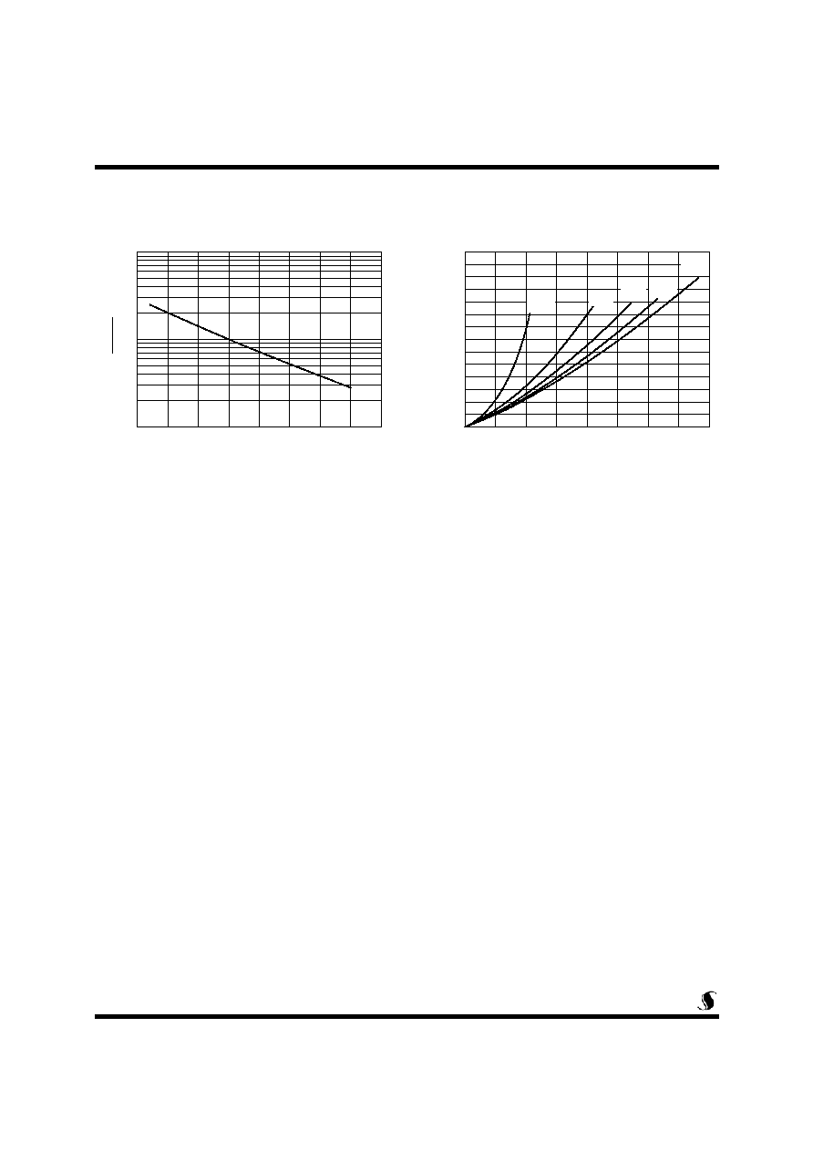
Fig 2. Maximum Case Temperature
: Conduction Angl e
360∞
2
Fig 3. Typical Forward Voltage
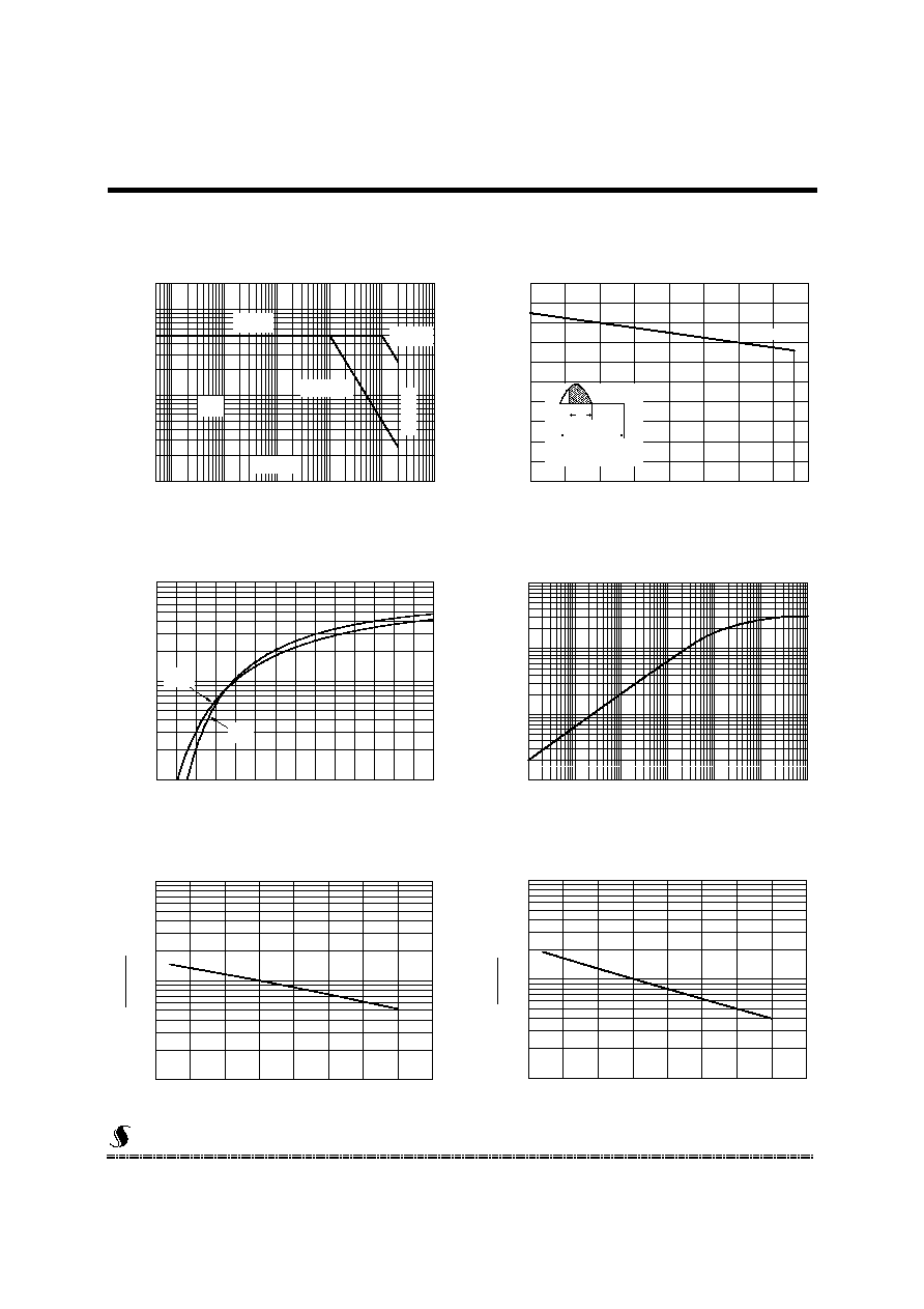
Fig 4. Thermal Response
Fig 5. Typical Gate Trigger Voltage vs.
Junction Temperature
Fig 6. Typical Gate Trigger Current vs.
Junction Temperature
3/5
SCR6C60
Fig 1. Gate Characteristics
-50
0
50
100
150
0.1
1
10
V
GT
(t
o
C)
V
GT
(25
o
C)
Junction Temperature[
o
C]