 | –≠–ª–µ–∫—Ç—Ä–æ–Ω–Ω—ã–π –∫–æ–º–ø–æ–Ω–µ–Ω—Ç: SC112 | –°–∫–∞—á–∞—Ç—å:  PDF PDF  ZIP ZIP |
© 2000 SEMTECH CORP.
652 MITCHELL ROAD NEWBURY PARK CA 91320
150mA ULTRA LOW DROPOUT
MICROPOWER LINEAR REGULATOR
SC112
PRELIMINARY - July 25, 2000
1
DESCRIPTION
The SC112 is a 150mA ultra low dropout linear
regulator with a built in CMOS/TTL logic level enable,
designed specifically for battery powered applications
where low quiescent current and low dropout are
critical for battery longevity.
The SC112 uses a Semtech proprietary internal PNP
device for the pass element, providing a low dropout
voltage of 130mV at a load of 60mA.
The output noise is reduced to 30µV (typical) by
placing a very low leakage 10nF capacitor on pin 3
(noise bypass).
Each device contains a bandgap reference, error
amplifier, PNP pass element, thermal and current
limiting circuitry and resistor divider network for setting
output voltage.
The SC112 is packaged in a six lead SOT-23 surface
mount package for a very small footprint and it requires
only a 1µF capacitor on the output and a 0.01µF on the
bypass pin for a minimum number of external
components.
FEATURES
∑
=
Low dropout voltage
∑
=
CMOS/TTL compatible control switch
∑
=
Very low quiescent current 60µA (ON, no load)
∑
=
Internal thermal shutdown
∑
=
Short circuit protection
∑
=
Very low standby current 0.1µA maximum (OFF)
∑
=
Low noise with external bypass capacitor
∑
=
Industrial temperature range
APPLICATIONS
∑
=
Battery powered systems
∑
=
Cellular telephones
∑
=
Cordless telephones
∑
=
Pagers, personal digital assistants
∑
=
Portable instrumentation
∑
=
Low voltage systems
TEL:805-498-2111 FAX:805-498-3804 WEB:http://www.semtech.com
DEVICE
(1)(2)
PACKAGE
SC112XXCSK.TR
6 pin SOT-23
ORDERING INFORMATION
Notes:
(1) Where XX denotes voltage options. Available volt-
ages are: 2.2V, 2.5V, 2.8V, 3.0V, 3.3V, 3.6V, 3.8V,
4.0V and 5.0V. Contact factory for additional voltage
options.
(2) Only available in tape and reel packaging. A reel
contains 3000 devices
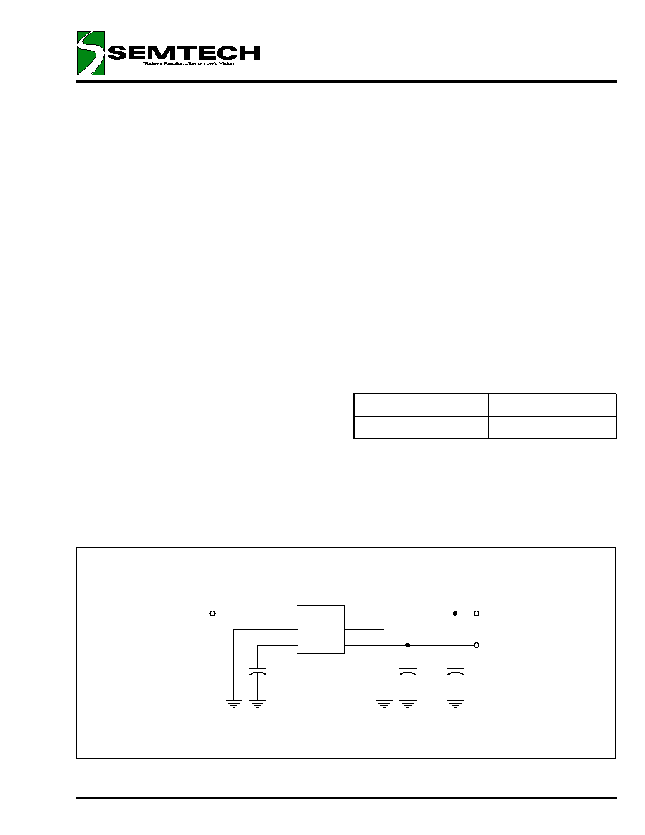
TYPICAL APPLICATION CIRCUIT
VIN
VO
EN
U1 SC112
1
2
3
4
5
6
EN
GND
BYP
VO
GND
VIN
C1
10nF
C2
1uF
C3
1uF

© 2000 SEMTECH CORP.
652 MITCHELL ROAD NEWBURY PARK CA 91320
150mA ULTRA LOW DROPOUT
MICROPOWER LINEAR REGULATOR
SC112
PRELIMINARY - July 25, 2000
2
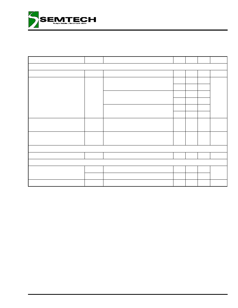
ELECTRICAL CHARACTERISTICS
Unless specified, T
A
= 25∞C, VIN = VO
(NOM)
+ 1V, C
IN
= 1µF, C
BYP
= 10nF, C
O
= 1µF.
Values in bold apply over full operating temperature range.
Parameter
Symbol
Test Conditions
MIN
TYP MAX
Units
VIN
Supply Voltage Range
VIN
2.5
14.5
V
Ground Pin Current
I
GND
I
O
= 0mA
60
75
µA
90
I
O
= 60mA
1.0
1.25
mA
1.5
I
O
= 100mA
2.1
2.5
3.0
I
O
= 150mA
4.2
4.75
5.25
V
IN
= 8V, Output OFF
0.1
µA
VO
Output Voltage
VO
I
O
= 30 mA
-2.5
VO
+2.5
%
-3.0
+3.0
Line Regulation
REG
(LINE)
VIN = (VO
(NOM)
+ 1V) to (VO
(NOM)
+ 6V),
5
10
mV
I
O
= 1mA
20
Load Regulation
REG
(LOAD)
I
O
= 1mA to 60mA
7.5
35
mV
I
O
= 1mA to 100mA
20
65
I
O
= 1mA to 150mA
35
110
Temperature Coefficient
VO/
T
I
O
= 10mA
40
ppm/∞C
ABSOLUTE MAXIMUM RATINGS
Parameter
Symbol
Maximum
Units
Input Supply Voltage
VIN
-0.3 to +16
V
Enable Input Voltage
V
EN
-0.3 to VIN
V
Power Dissipation
P
D
Internally Limited
W
Thermal Resistance Junction to Ambient
JA
230
∞C/W
Operating Ambient Temperature Range
T
A
-40 to +85
∞C
Operating Junction Temperature Range
T
A
-40 to +125
∞C
Storage Temperature Range
T
STG
-55 to +150
∞C
Lead Temperature (Soldering) 10 sec.
T
LEAD
300
∞C
ESD Rating
ESD
2
kV
© 2000 SEMTECH CORP.
652 MITCHELL ROAD NEWBURY PARK CA 91320
150mA ULTRA LOW DROPOUT
MICROPOWER LINEAR REGULATOR
SC112
PRELIMINARY - July 25, 2000
3
ELECTRICAL CHARACTERISTICS
Unless specified, T
A
= 25∞C, VIN = VO
(NOM)
+ 1V, C
IN
= 1µF, C
BYP
= 10nF, C
O
= 1µF.
Values in bold apply over full operating temperature range.
Parameter
Symbol
Test Conditions
MIN
TYP MAX
Units
VO (Cont.)
Current Limit
(1)
I
LIM
180
200
mA
Dropout Voltage
V
D
I
O
= 60mA
130
150
mV
180
I
O
= 100mA
165
195
225
I
O
= 150mA
200
245
275
Power Supply Rejection Ratio
RR
V
RIPPLE
= 100mV(rms), f = 400Hz,
60
dB
I
O
= 30mA
Output Noise Voltage
e
n
10 Hz
f
80 kHz,
30
µV(rms)
I
O
= 60mA
BYP
Noise Bypass Terminal Voltage
V
BYP
1.250
V
EN
Enable Input Threshold Voltage
V
IH
Output ON
1.8
V
V
IL
Output OFF
0.5
Enable Input Bias Current
I
EN
V
EN
= 1.8V, Output ON
6
10
µA
NOTE:
(1) As the load resistance further decreases, the SC112 folds back the output current to approximately 100mA at
VO = 0V.

© 2000 SEMTECH CORP.
652 MITCHELL ROAD NEWBURY PARK CA 91320
150mA ULTRA LOW DROPOUT
MICROPOWER LINEAR REGULATOR
SC112
PRELIMINARY - July 25, 2000
4
BLOCK DIAGRAM
PIN CONFIGURATION
PIN DESCRIPTION
Pin #
Pin Name
Description
1
EN
Active high enable pin. Connect to VIN if not being used.
2
GND
Ground pin. Use for heatsinking along with Pin #5.
3
BYP
Noise bypass pin. Connect a 10nF capacitor (required) between this pin and GND.
4
VO
Regulator output, supplying a guaranteed 150mA.
5
GND
Ground pin. Use for heatsinking along with Pin #2.
6
VIN
Power input pin.
Top View
SOT-23-6L
APPLICATION HINTS (Refer to Sheet 1):
(1) C
IN
(C3) is needed if the device is far from the supply's filter capac-
itors, or for operation from a battery. A value of 1.0µF or greater should
be used. C
IN
may be tantalum or ceramic.
(2) C
O
(C2) should be a 1µF or greater tantalum or ceramic capacitor,
with an Equivalent Series Resistance (ESR) between 10m
and 1
over temperature. Larger value capacitors will improve the overall tran-
sient response.
(3) C
BYP
(C1 - required) should be placed as close as possible to pin 3
and ground. A 10nF ceramic capacitor is recommended.
(4) EN may be tied to V
IN
if the shutdown feature is not required. Maxi-
mum EN voltage = V
IN
.
(5) Connect both ground pins (2 and 5) to ground to maximize heat
conduction.
© 2000 SEMTECH CORP.
652 MITCHELL ROAD NEWBURY PARK CA 91320
150mA ULTRA LOW DROPOUT
MICROPOWER LINEAR REGULATOR
SC112
PRELIMINARY - July 25, 2000
5
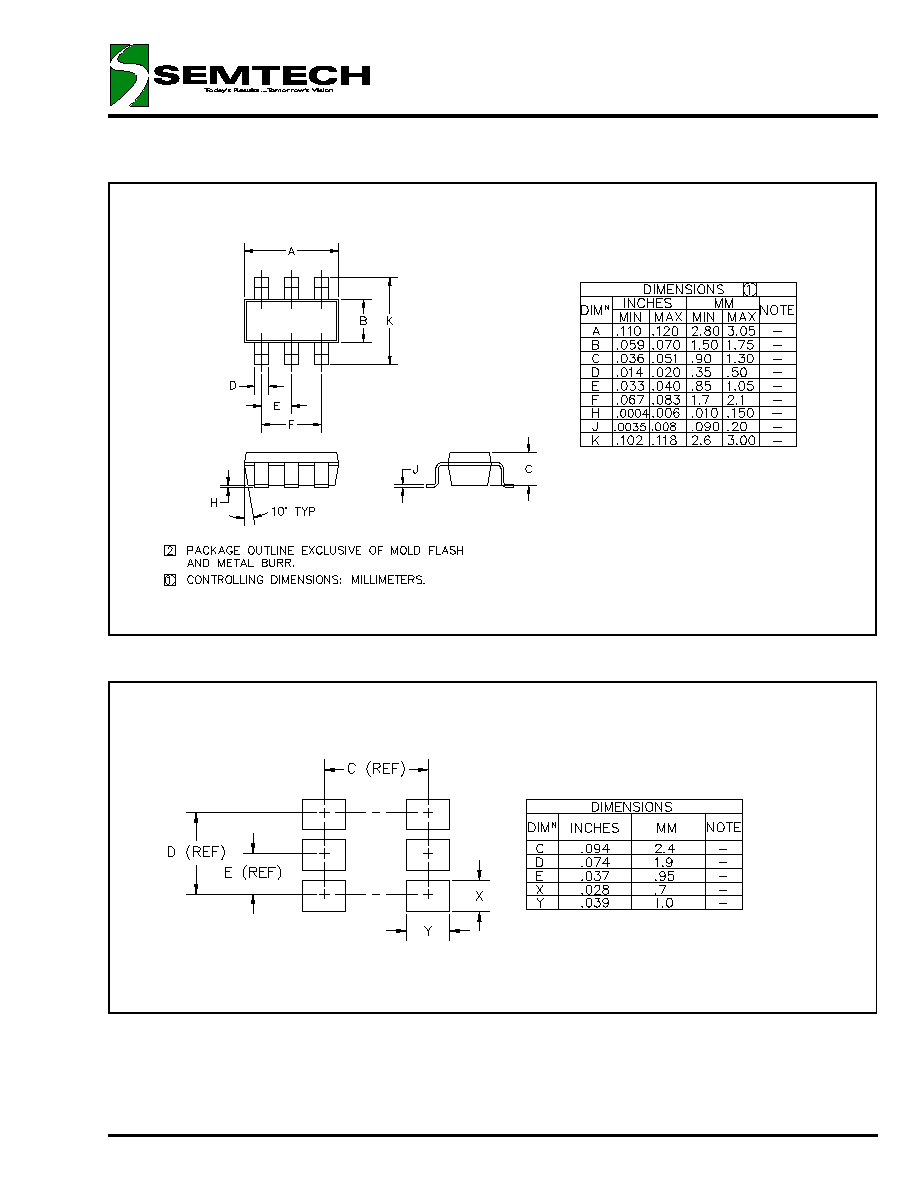
DEVICE OUTLINE - SOT23-6L
MINIMUM LAND PATTERN - SOT23-6L
ECN00-1203