1
www.semtech.com
SC1301A/B
2A High Speed Low-Side
MOSFET Driver in SOT-23
POWER MANAGEMENT
Revision: July 18, 2003
Description
Features
Applications
Typical Application Circuit
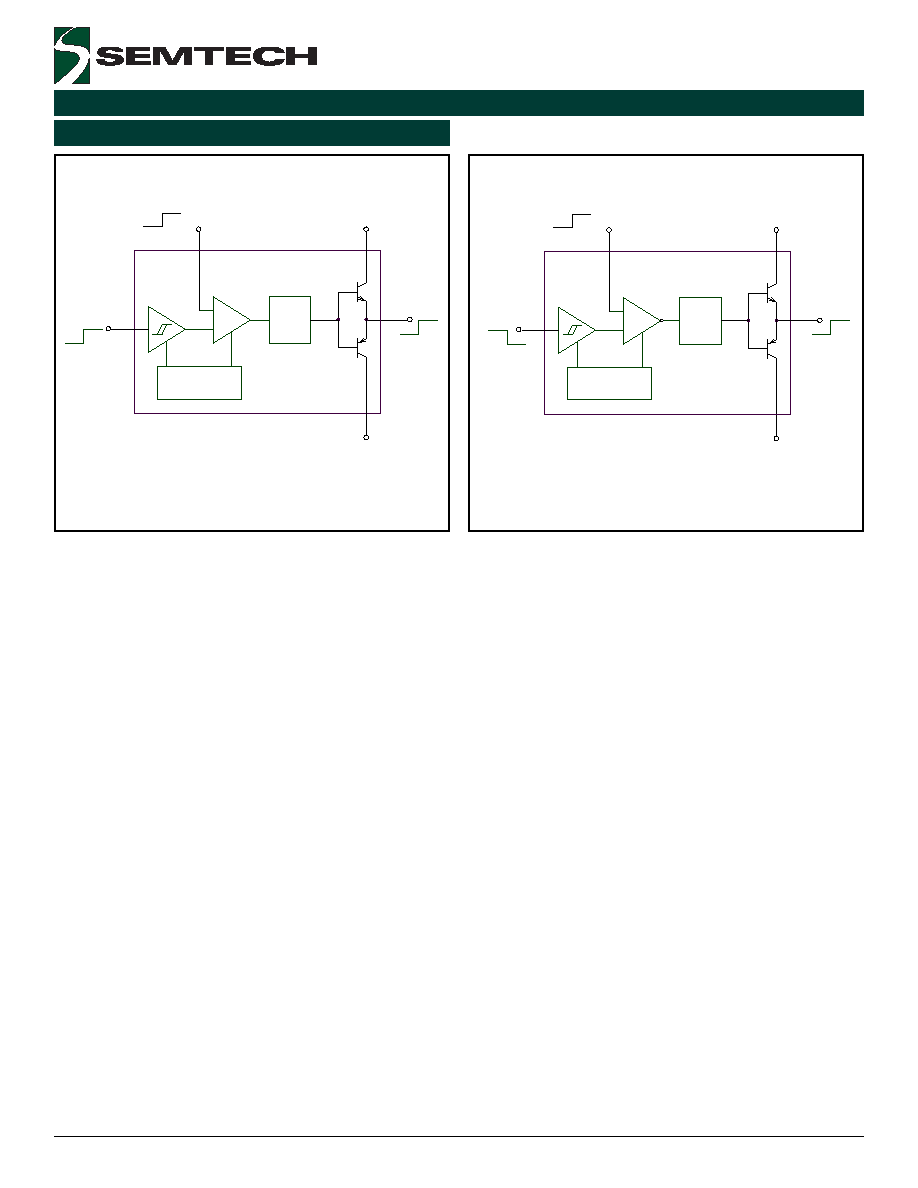
The SC1301A/B is a cost effective single-channel high-
speed MOSFET driver. The driver is capable of driving a
1000pF load in 20ns rise/fall time and has a 60ns propa-
gation delay time from input transition to the gate of the
power MOSFET. The high current driving capability
(2A peak) allows fast switching up to 1MHz. The SC1301A
is noninverting and the SC1301B is inverting.
An Undervoltage lockout circuit is included to guarantee
that the driver output is low when Vcc is less than or
equal to 4.1V (typ) at supply ramp up. An internal tem-
perature sensor shuts down the driver in the event of
overtemperature. The 5-pin SOT-23 package uses mini-
mum space.
+4.5V to +16.5V operation
Fast rise and fall times
(20ns typical with 1000pf load )
2A peak drive current
5-pin SOT-23 package
Enable/disable control
TTL-compatible input
Inverting or noninverting versions
Undervoltage lockout
Low supply current
-40°C to 85°C ambient temperature operating range
Over temperature protection
ESD protection
Switch-mode power supplies
Battery powered applications
Solenoid and motor drives
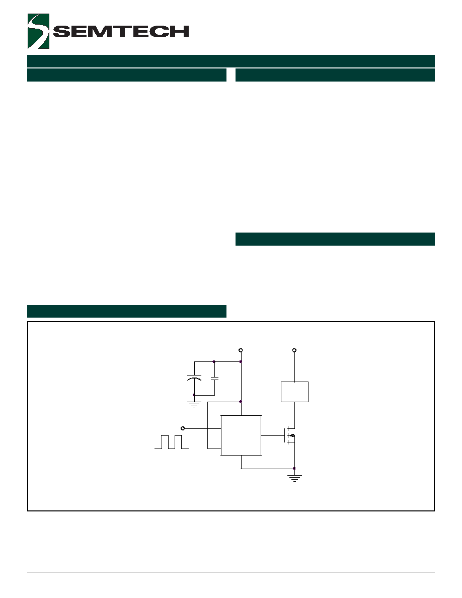
SC1301A
3
1
4
2
5
VC
C
IN
OUT
GN
D
EN
Vload
Input
10uF
LOAD
0.1uF
+12V
2
2003 Semtech Corp.
www.semtech.com
SC1301A/B
PRELIMINARY
POWER MANAGEMENT
Absolute Maximum Ratings
Unless otherwise specified: T
A
=
25°C, V
CC
= 12V, V
IN
= 5V, V
EN
= 5V
r
e
t
e
m
a
r
a
P
l
o
b
m
y
S
s
n
o
i
t
i
d
n
o
C
n
i
M
p
y
T
x
a
M
s
t
i
n
U
t
n
e
r
r
u
C
y
l
p
p
u
S
t
n
e
r
r
u
C
t
n
e
c
s
e
i
u
Q
I
Q
V
N
I
A
1
0
3
1
C
S
r
o
f
V
0
=
0
.
3
0
.
4
A
m
V
N
I
B
1
0
3
1
C
S
r
o
f
V
5
=
0
.
3
0
.
4
t
u
o
k
c
o
L
e
g
a
t
l
o
V
-
r
e
d
n
U
e
g
a
tl
o
V
d
l
o
h
s
e
r
h
T
V
C
C
9
.
3
1
.
4
4
.
4
V
e
l
b
a
n
E
e
g
a
tl
o
V
e
l
b
a
n
E
V
N
E
V
<
0
N
E
c
c
V
<
0
.
2
V
e
g
a
tl
o
V
e
l
b
a
s
i
D
V
N
E
V
<
0
N
E
c
c
V
<
8
.
0
V
t
u
p
t
u
O
o
t
y
a
l
e
D
t
N
E
_
D
h
g
i
h
o
t
w
o
l
m
o
r
f
N
E
0
6
S
n
t
u
p
t
u
O
o
t
y
a
l
e
D
t
S
I
D
_
D
w
o
l
o
t
h
g
i
h
m
o
r
f
N
E
0
4
S
n
t
n
e
r
r
u
C
t
u
p
n
I
e
l
b
a
n
E
I
N
E
V
<
0
N
E
c
c
V
<
5
2
1
A
µ
t
u
p
n
I
e
g
a
tl
o
V
t
u
p
n
I
l
e
v
e
L
h
g
i
H
V
H
I
V
<
0
N
I
c
c
V
<
0
.
2
V
e
g
a
tl
o
V
t
u
p
n
I
l
e
v
e
L
w
o
L
V
L
I
V
<
0
N
I
c
c
V
<
8
.
0
V
t
n
e
r
r
u
C
t
u
p
n
I
I
N
I
V
<
0
N
I
c
c
V
<
5
2
1
A
µ
r
e
t
e
m
a
r
a
P
l
o
b
m
y
S
x
a
M
s
t
i
n
U
e
g
a
tl
o
V
y
l
p
p
u
S
c
c
V
0
2
V
e
g
a
tl
o
V
y
l
p
p
u
S
g
n
it
a
r
e
p
O
c
c
V
5
.
6
1
V
e
g
a
tl
o
V
t
u
p
n
I
V
N
I
c
c
V
V
e
g
a
tl
o
V
t
u
p
t
u
O
V
T
U
O
c
c
V
V
e
g
a
tl
o
V
e
l
b
a
n
E
V
N
E
c
c
V
V
n
o
it
a
p
i
s
s
i
D
r
e
w
o
P
s
u
o
u
n
it
n
o
C
d
P
d
e
ti
m
il
y
ll
a
n
r
e
t
n
I
W
t
n
e
i
b
m
A
o
t
n
o
it
c
n
u
J
e
c
n
a
t
s
i
s
e
R
l
a
m
r
e
h
T
0
6
2
W
/
C
°
e
g
n
a
R
e
r
u
t
a
r
e
p
m
e
T
g
n
it
a
r
e
p
O
T
A
5
8
+
o
t
0
4
-
C
°
e
g
n
a
R
e
r
u
t
a
r
e
p
m
e
T
e
g
a
r
o
t
S
T
G
T
S
0
5
1
+
o
t
5
6
-
C
°
c
e
s
0
1
)
g
n
ir
e
d
l
o
S
(
e
r
u
t
a
r
e
p
m
e
T
d
a
e
L
T
D
A
E
L
0
6
2
C
°
)l
e
d
o
M
y
d
o
B
n
a
m
u
H
(
g
n
it
a
R
D
S
E
D
S
E
3
V
k
DC Electrical Characteristics
Exceeding the specifications below may result in permanent damage to the device, or device malfunction. Operation outside of the parameters specified
in the Electrical Characteristics section is not implied.
3
2003 Semtech Corp.
www.semtech.com
SC1301A/B
POWER MANAGEMENT
Timing Diagrams
r
e
t
e
m
a
r
a
P
l
o
b
m
y
S
s
n
o
i
t
i
d
n
o
C
n
i
M
p
y
T
x
a
M
s
t
i
n
U
e
m
it
e
s
i
R
t
R
m
a
r
g
a
i
D
g
n
i
m
i
T
e
e
S
0
2
s
n
e
m
it
ll
a
F
t
F
m
a
r
g
a
i
D
g
n
i
m
i
T
e
e
S
0
2
s
n
e
m
it
y
a
l
e
d
n
o
it
a
g
a
p
o
r
P
t
1
D
m
a
r
g
a
i
D
g
n
i
m
i
T
e
e
S
0
6
s
n
e
m
it
y
a
l
e
d
n
o
it
a
g
a
p
o
r
P
t
2
D
m
a
r
g
a
i
D
g
n
i
m
i
T
e
e
S
0
6
s
n
AC Electrical Characteristics
Unless otherwise specified: T
A
=
25°C, V
CC
= 12V
,
V
EN
= 5V, C
L
= 1000pF
r
e
t
e
m
a
r
a
P
l
o
b
m
y
S
s
n
o
i
t
i
d
n
o
C
n
i
M
p
y
T
x
a
M
s
t
i
n
U
t
u
p
t
u
O
t
n
e
r
r
u
C
k
a
e
P
t
u
p
t
u
O
I
E
C
R
U
O
S
_
K
P
V
T
U
O
t
,
V
5
.
0
=
W
P
,
S
µ
0
1
<
e
s
l
u
p
e
l
g
n
i
s
2
A
I
K
N
I
S
_
K
P
V
T
U
O
t
,
V
5
.
0
-
c
c
V
=
W
P
,
S
µ
0
1
<
e
s
l
u
p
e
l
g
n
i
s
2
A
n
w
o
d
t
u
h
S
l
a
m
r
e
h
T
t
n
i
o
P
p
ir
T
e
r
u
t
a
r
e
p
m
e
T
r
e
v
O
T
T
O
_
J
0
5
1
C
°
DC Electrical Characteristics (Cont.)
Unless otherwise specified: T
A
=
25°C, V
CC
= 12V
,
V
IN
= 5V, V
EN
= 5V
90%
10%
90%
10%
90%
10%
10%
90%
10%
90%
t
R
t
F
t
F
t
R
t
D1
t
D2
Input
Non-inverted
Output
SC1301A
Inverted
Output
SC1301B
0V
5V
4
2003 Semtech Corp.
www.semtech.com
SC1301A/B
PRELIMINARY
POWER MANAGEMENT
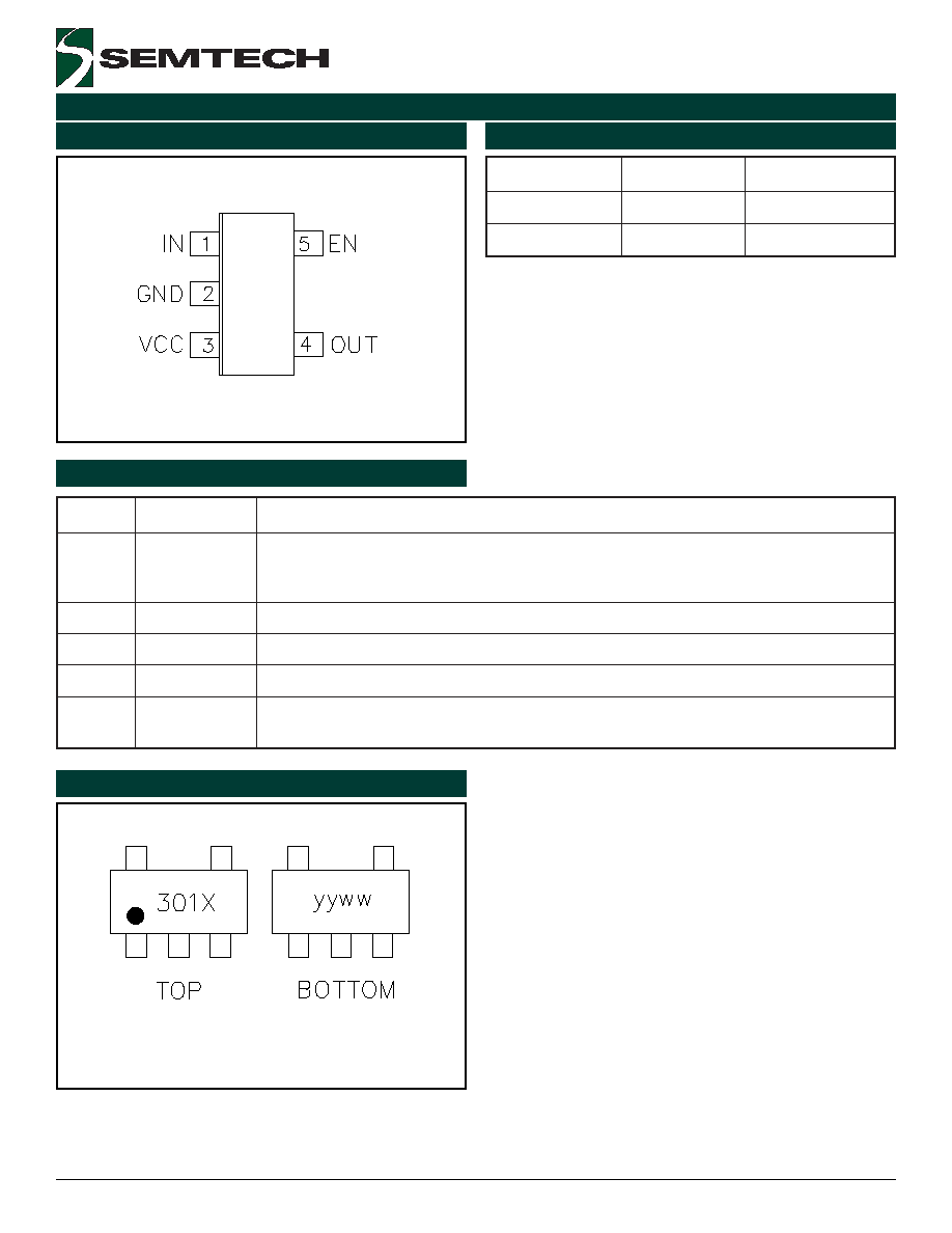
Pin Descriptions
Pin Configuration
Ordering Information
#
n
i
P
e
m
a
N
n
i
P
n
o
i
t
c
n
u
F
n
i
P
1
N
I
.r
e
v
ir
d
e
h
t
o
t
l
a
n
g
i
s
t
u
p
n
i
e
l
b
it
a
p
m
o
c
-
L
T
T
.
D
N
G
e
h
t
o
t
T
U
O
e
h
t
s
e
c
r
o
f
w
o
l
c
i
g
o
L
.
C
C
V
e
h
t
o
t
T
U
O
e
h
t
s
e
c
r
o
f
h
g
i
h
c
i
g
o
L
:
A
1
0
3
1
C
S
.
C
C
V
e
h
t
o
t
T
U
O
e
h
t
s
e
c
r
o
f
w
o
l
c
i
g
o
L
.
D
N
G
e
h
t
o
t
T
U
O
e
h
t
s
e
c
r
o
f
h
g
i
h
c
i
g
o
L
:
B
1
0
3
1
C
S
2
D
N
G
.
d
n
u
o
r
G
3
C
C
V
.
w
o
l
d
l
e
h
s
i
T
U
P
T
U
O
e
h
t
,
O
L
V
U
g
n
ir
u
D
.
y
l
p
p
u
s
V
5
.
6
1
+
o
t
V
5
.
4
+
:
y
l
p
p
u
S
4
T
U
O
.
T
E
F
S
O
M
g
n
i
h
c
ti
w
s
e
h
t
r
o
f
e
v
ir
d
e
t
a
g
t
u
p
t
u
O
5
N
E
e
h
t
,
n
e
p
o
tf
e
l
n
e
h
W
.
w
o
l
s
i
T
U
P
T
U
O
e
h
t
,
w
o
l
n
e
v
ir
d
s
i
N
E
e
h
t
n
e
h
W
.l
o
r
t
n
o
c
e
l
b
a
s
i
d
/
e
l
b
a
n
E
.
w
o
l
s
i
T
U
P
T
U
O
r
e
b
m
u
N
t
r
a
P
e
g
a
k
c
a
P
T
(
e
g
n
a
R
.
p
m
e
T
J
)
R
T
K
S
I
A
1
0
3
1
C
S
5
-
3
2
-
T
O
S
C
°
5
2
1
+
o
t
C
°
0
4
-
R
T
K
S
I
B
1
0
3
1
C
S
5
-
3
2
-
T
O
S
C
°
5
2
1
+
o
t
C
°
0
4
-
Note:
Only available in tape and reel packaging. A reel
contains 3000 devices.
Top View
(SOT-23-5L)
Marking Information
301X = 301A or 301B (Example: 301A)
yyww = Datecode (Example: 0050)