1
www.semtech.com
POWER MANAGEMENT
SC1302A/B/C/D/E/F
Dual High Speed Low-Side
MOSFET Driver
Revision: December 2, 2004
Description
Features
Applications
+4.5V to +16.5V operation
Fast rise and fall times (20ns typical with 1000pf
load)
Dual MOSFET driver
2A peak drive current
40ns propagation delay
8-pin SOIC / MSOP packages
Enable/disable control
TTL-compatible input
Under voltage lockout with hysteresis
Low shutdown supply current
Over temperature protection
ESD protection
Dual inverting/non-inverting and inverting/non-invert-
ing configurations
Switch-mode power supplies
Battery powered applications
Solenoid and motor drives
Typical Application Circuit
S C 1 3 0 2 A
6
2
4
5
1
V C C
IN A
O U TA
G N D
E N
1 0 u F
0 .1 u F
In p u tA
+ 1 2 V
IN B
O U TB
S H D N
7
3
8
L o a d A
L o a d B
V lo a d
In p u tB
The SC1302A/B/C/D/E/F family are low cost dual low-
side MOSFET drivers. These drivers accept TTL-compat-
ible inputs and are capable of supplying high current
outputs (> 2A peak) to external MOSFETs. Fast switch-
ing allows operation up to 1 MHz. The SC1302A/B/C is
available in six configurations: SC1302A is a dual non-
inverting, SC1302B is a dual inverting and SC1302C is a
one inverting plus one non-inverting output.
The SC1302D/E/F is the derivative part from SC1302A/
B/C with pin 1 (EN) and pin 8 (SHDN) internally tied to
VCC.
An under-voltage lockout circuit guarantees that the
driver outputs are low when Vcc is less than 4.5V (typ).
An internal temperature sensor shuts down the driver in
the event of over temperature.
2
2004 Semtech Corp.
www.semtech.com
SC1302A/B/C/D/E/F
PRELIMINARY
POWER MANAGEMENT
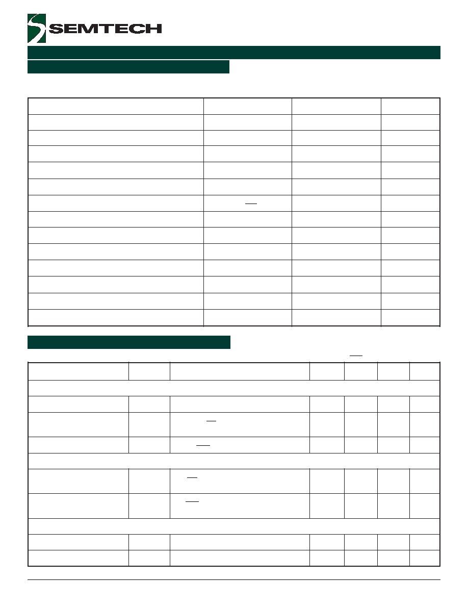
Absolute Maximum Ratings
DC Electrical Characteristics
Unless otherwise specified:
-40�C < T
A
< 85�C, V
CC
= 12V, V
IN
= 5V, V
EN
= 5V (SC1302A/B/C) , V
SHDN
= 5V (SC1302A/B/C).
r
e
t
e
m
a
r
a
P
l
o
b
m
y
S
s
n
o
i
t
i
d
n
o
C
n
i
M
p
y
T
x
a
M
s
t
i
n
U
t
n
e
r
r
u
C
y
l
p
p
u
S
t
n
e
r
r
u
C
t
n
e
c
s
e
i
u
Q
I
Q
V
C
C
V
<
T
R
A
T
S
1
8
.
1
A
m
t
n
e
r
r
u
C
t
n
e
c
s
e
i
u
Q
I
Q
V
N
E
V
=
N
D
H
S
,
C
/
B
/
A
2
0
3
1
C
S
r
o
f
V
3
=
V
A
N
I
V
=
B
N
I
V
3
=
7
.
5
1
.
8
A
m
t
n
e
r
r
u
C
t
n
e
c
s
e
i
u
Q
I
Q
V
N
D
H
S
C
/
B
/
A
2
0
3
1
C
S
r
o
f
V
0
=
3
8
A
�
t
u
o
k
c
o
L
e
g
a
t
l
o
V
-
r
e
d
n
U
e
g
a
tl
o
V
d
l
o
h
s
e
r
h
T
V
T
R
A
T
S
V
N
D
H
S
V
=
N
E
,
C
/
B
/
A
2
0
3
1
C
S
r
o
f
V
3
=
V
A
N
I
V
=
B
N
I
V
3
=
2
.
4
5
.
4
7
.
4
V
s
i
s
e
r
e
t
s
y
H
V
N
D
H
S
V
=
N
E
,
C
/
B
/
A
2
0
3
1
C
S
r
o
f
V
3
=
V
A
N
I
V
=
B
N
I
V
3
=
0
5
2
0
2
3
5
7
4
V
m
e
l
b
a
n
E
C
/
B
/
A
2
0
3
1
C
S
r
o
f
e
g
a
tl
o
V
e
l
b
a
n
E
V
N
E
V
<
0
N
E
V
<
C
C
0
.
2
V
e
g
a
tl
o
V
e
l
b
a
s
i
D
V
N
E
V
<
0
N
E
V
<
C
C
8
.
0
V
Exceeding the specifications below may result in permanent damage to the device, or device malfunction. Operation outside of the parameters specified
in the Electrical Characteristics section is not implied. Exposure to Absolute Maximum rated conditions for extended periods of time may affect device
reliability.
r
e
t
e
m
a
r
a
P
l
o
b
m
y
S
p
y
T
s
t
i
n
U
e
g
a
tl
o
V
y
l
p
p
u
S
V
C
C
0
2
o
t
3
.
0
-
V
e
g
a
tl
o
V
y
l
p
p
u
S
g
n
it
a
r
e
p
O
V
C
C
5
.
6
1
o
t
3
.
0
-
V
s
e
g
a
tl
o
V
t
u
p
n
I
V
,
A
N
I
V
B
N
I
V
o
t
3
.
0
-
C
C
V
s
t
n
e
r
r
u
C
t
u
p
t
u
O
k
a
e
P
I
,
A
T
U
O
I
B
T
U
O
3
A
)
C
/
B
/
A
2
0
3
1
C
S
(
e
g
a
tl
o
V
e
l
b
a
n
E
V
N
E
V
o
t
3
.
0
-
C
C
V
)
C
/
B
/
A
2
0
3
1
C
S
(
e
g
a
tl
o
V
n
w
o
d
t
u
h
S
V
N
D
H
S
V
o
t
3
.
0
-
C
C
V
n
o
it
a
p
i
s
s
i
D
r
e
w
o
P
s
u
o
u
n
it
n
o
C
d
P
d
e
ti
m
il
y
ll
a
n
r
e
t
n
I
W
e
g
n
a
R
e
r
u
t
a
r
e
p
m
e
T
g
n
it
a
r
e
p
O
T
A
5
8
+
o
t
0
4
-
C
�
)
P
O
S
M
(
t
n
e
i
b
m
A
o
t
n
o
it
c
n
u
J
e
c
n
a
t
s
i
s
e
R
l
a
m
r
e
h
T
A
J
6
0
2
W
/
C
�
)
C
I
O
S
(
t
n
e
i
b
m
A
o
t
n
o
it
c
n
u
J
e
c
n
a
t
s
i
s
e
R
l
a
m
r
e
h
T
A
J
5
6
1
W
/
C
�
e
g
n
a
R
e
r
u
t
a
r
e
p
m
e
T
e
g
a
r
o
t
S
T
G
T
S
0
5
1
+
o
t
5
6
-
C
�
c
e
s
0
1
)
g
n
i
r
e
d
l
o
S
(
e
r
u
t
a
r
e
p
m
e
T
d
a
e
L
T
D
A
E
L
0
6
2
C
�
)l
e
d
o
M
y
d
o
B
n
a
m
u
H
(
g
n
it
a
R
D
S
E
D
S
E
2
V
k
3
2004 Semtech Corp.
www.semtech.com
POWER MANAGEMENT
SC1302A/B/C/D/E/F
r
e
t
e
m
a
r
a
P
l
o
b
m
y
S
s
n
o
i
t
i
d
n
o
C
n
i
M
p
y
T
x
a
M
s
t
i
n
U
e
m
it
e
s
i
R
)
1
(
t
R
m
a
r
g
a
i
D
g
n
i
m
i
T
e
e
S
0
2
s
n
e
m
it
ll
a
F
)
1
(
t
F
m
a
r
g
a
i
D
g
n
i
m
i
T
e
e
S
0
2
s
n
e
m
it
y
a
l
e
d
n
o
it
a
g
a
p
o
r
P
)
1
(
t
1
D
m
a
r
g
a
i
D
g
n
i
m
i
T
e
e
S
3
5
s
n
e
m
it
y
a
l
e
d
n
o
it
a
g
a
p
o
r
P
)
1
(
t
2
D
m
a
r
g
a
i
D
g
n
i
m
i
T
e
e
S
1
4
s
n
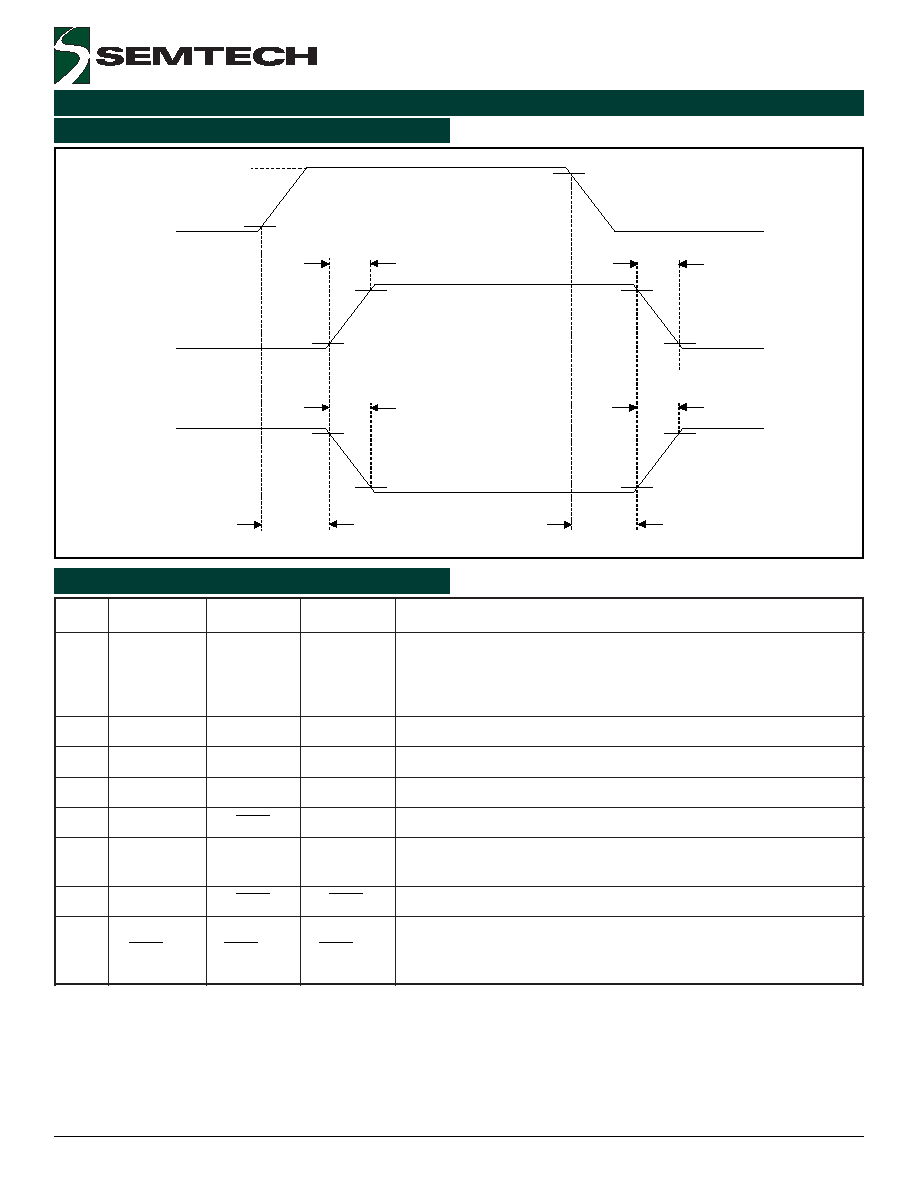
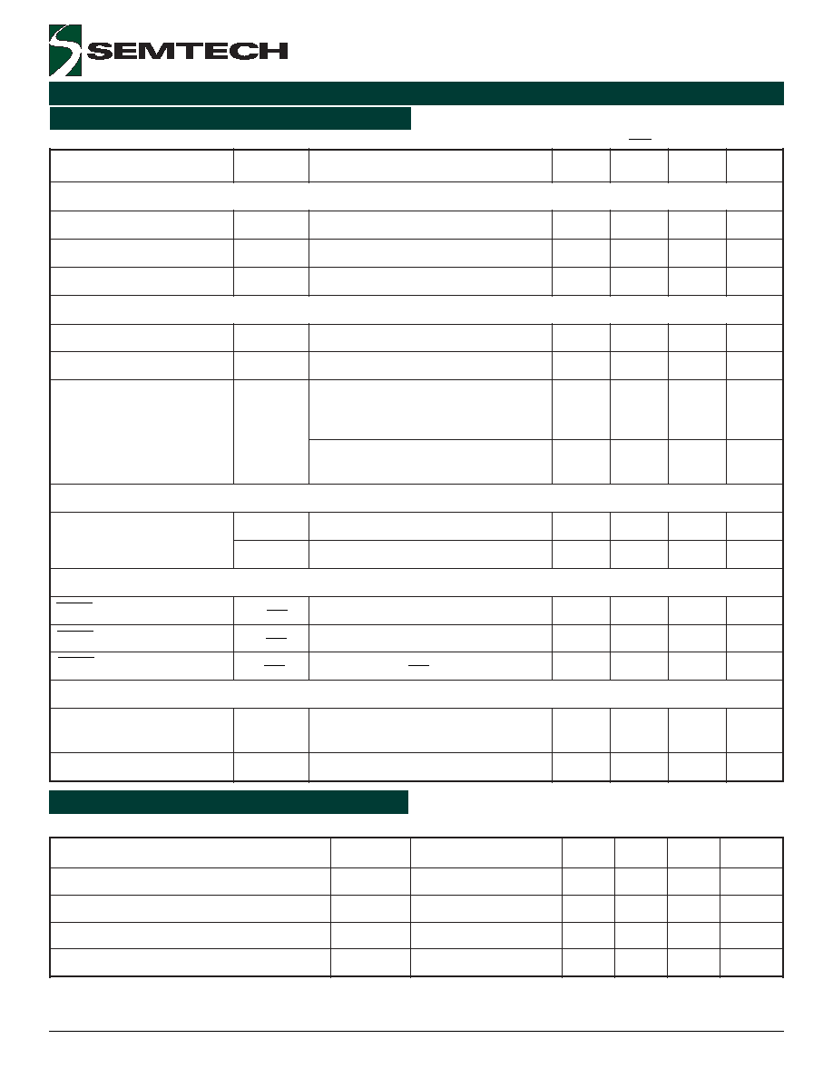
AC Electrical Characteristics
Unless otherwise specified: T
A
=
25�C, V
CC
= 12V, V
EN
= 5V, C
L
= 1000pF
DC Electrical Characteristics (Cont.)
Notes:
(1) Guaranteed by design not tested in production.
(2) Negative sign indicates that the input current flows out of the device.
r
e
t
e
m
a
r
a
P
l
o
b
m
y
S
s
n
o
i
t
i
d
n
o
C
n
i
M
p
y
T
x
a
M
s
t
i
n
U
)
.
t
n
o
C
(
C
/
B
/
A
2
0
3
1
C
S
r
o
f
e
l
b
a
n
E
t
u
p
t
u
O
o
t
y
a
l
e
D
)
1
(
t
N
E
_
D
h
g
i
h
o
t
w
o
l
r
o
f
N
E
0
7
s
n
t
u
p
t
u
O
o
t
y
a
l
e
D
)
1
(
t
S
I
D
_
D
w
o
l
o
t
h
g
i
h
m
o
r
f
N
E
5
5
s
n
t
n
e
r
r
u
C
t
u
p
n
I
e
l
b
a
n
E
N
E
I
V
<
0
N
I
V
<
C
C
0
1
4
1
9
1
A
�
t
u
p
n
I
e
g
a
tl
o
V
t
u
p
n
I
l
e
v
e
L
h
g
i
H
V
H
I
V
<
0
N
I
V
<
C
C
0
.
2
V
e
g
a
tl
o
V
t
u
p
n
I
l
e
v
e
L
w
o
L
V
L
I
V
<
0
N
I
V
<
C
C
8
.
0
V
t
n
e
r
r
u
C
t
u
p
n
I
I
N
I
V
<
0
N
I
V
<
C
C
f
o
)
s
(
t
u
p
n
I
g
n
it
r
e
v
n
I
-
n
o
N
F
/
D
/
C
/
A
2
0
3
1
C
S
3
1
5
.
8
1
A
�
V
<
0
N
I
V
<
C
C
F
/
E
/
C
/
B
2
0
3
1
C
S
f
o
)
s
(
t
u
p
n
I
g
n
it
r
e
v
n
I
)
2
(
8
-
A
�
t
u
p
t
u
O
t
n
e
r
r
u
C
k
a
e
P
t
u
p
t
u
O
I
E
C
R
U
O
S
_
K
P
V
T
U
O
t
,
V
5
.
0
=
W
P
S
u
0
1
<
0
0
6
1
A
m
I
K
N
I
S
_
K
P
V
T
U
O
V
=
C
C
t
,
V
5
.
0
-
W
P
S
u
0
1
<
0
0
6
1
A
m
)
.
t
n
o
C
(
C
/
B
/
A
2
0
3
1
C
S
n
w
o
d
t
u
h
S
h
g
i
H
e
g
a
tl
o
V
t
u
p
n
I
N
D
H
S
V
N
D
H
S
2
V
w
o
L
e
g
a
tl
o
V
t
u
p
n
I
N
D
H
S
V
N
D
H
S
3
.
0
V
t
n
e
r
r
u
C
n
i
P
N
D
H
S
I
N
D
H
S
V
N
D
H
S
V
5
=
2
3
0
4
A
�
n
w
o
d
t
u
h
S
l
a
m
r
e
h
T
p
ir
T
e
r
u
t
a
r
e
p
m
e
T
r
e
v
O
t
n
i
o
P
)
1
(
T
T
O
_
J
0
5
1
C
�
s
i
s
e
r
e
t
s
y
H
)
1
(
0
1
C
�
Unless otherwise specified:
-40�C < T
A
< 85�C, V
CC
= 12V, V
IN
= 5V, V
EN
= 5V (SC1302A/B/C) , V
SHDN
= 5V (SC1302A/B/C).
5
2004 Semtech Corp.
www.semtech.com
POWER MANAGEMENT
SC1302A/B/C/D/E/F
Pin Configuration
Ordering Information
r
e
b
m
u
N
t
r
a
P
)
2
(
e
g
a
k
c
a
P
)
1
(
T
(
e
g
n
a
R
.
p
m
e
T
A
)
T
R
T
S
I
A
2
0
3
1
C
S
8
-
C
I
O
S
C
�
5
8
+
o
t
C
�
0
4
-
T
R
T
S
I
B
2
0
3
1
C
S
T
R
T
S
I
C
2
0
3
1
C
S
T
R
T
S
D
2
0
3
1
C
S
T
R
T
S
E
2
0
3
1
C
S
T
R
T
S
F
2
0
3
1
C
S
T
R
T
S
M
I
A
2
0
3
1
C
S
8
-
P
O
S
M
C
�
5
8
+
o
t
C
�
0
4
-
T
R
T
S
M
I
B
2
0
3
1
C
S
T
R
T
S
M
I
C
2
0
3
1
C
S
Notes:
(1) Only available in tape and reel packaging. A reel
contains 2500 devices.
(2) Lead free product.This product is fully WEEE and
RoHS compliant.
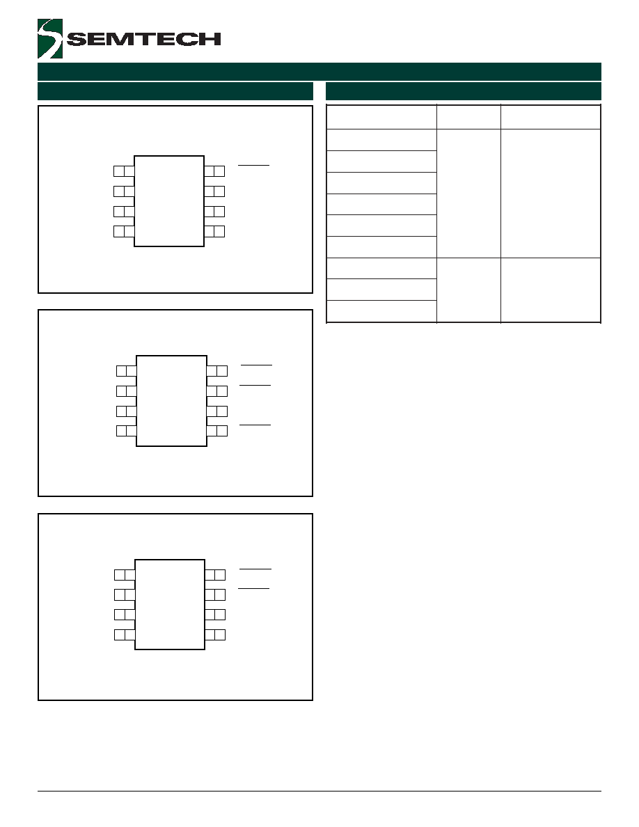
Top View
SC1302A/D (Dual Non-Inverting)
(8-Pin SOIC (A/D)
or MSOP (A only)
Top View
SC1302C/F (Inverting + Non-Inverting)
Top View
SC1302B/E (Dual Inverting)
1
2
3
4
SHDN/NC
EN/NC
5
6
7
8
OUTA
INA
VCC
GND
OUTB
INB
1
2
3
4
SHDN/NC
EN/NC
5
6
7
8
OUTA
INA
VCC
GND
OUTB
INB
1
2
3
4
SHDN/NC
EN/NC
5
6
7
8
OUTA
INA
VCC
GND
OUTB
INB
(8-Pin SOIC (B/E)
or MSOP (B only)
(8-Pin SOIC (C/F)
or MSOP (C only)