1
www.semtech.com
SC1454
Dual 150mA Ultra Low
Dropout, Low Noise Regulator
POWER MANAGEMENT
Revision 1, November 2000
The SC1454 contains two ultra low dropout voltage
regulators (ULDOs). It operates from an input voltage
range of 2.25V to 6.5V, and a wide variety of output
voltage options are available. One ULDO has a fixed
output, and the other is either fixed (SETA pin grounded)
or adjustable using external resistors. Each ULDO has an
independent enable pin.
The SC1454 has a bypass pin to enable the user to
capacitively decouple the bandgap reference for very low
output noise (50µV
RMS
typically).
Designed specifically for battery operated systems, the
devices utilize CMOS technology to require very low
operating currents (typically 130µA with both outputs
supplying 150mA). In addition, the dropout voltage is
typically 155mV at 150mA, helping to prolong battery
life further. The devices are designed to provide 400mA
of peak current for applications which require high initial
inrush current.
They have been designed to be used with low ESR
ceramic capacitors to save cost and PCB area.
The SC1454 is available with a wide variety of voltage
options as standard. It comes in the tiny 8 lead MSOP
surface mount package.
u
Up to 150mA per regulator output
u
Low quiescent current
u
Low dropout voltage
u
Stable operation with ceramic caps
u
Very low 50µV
RMS
output noise
u
Wide selection of output voltages
u
Tight load and line regulation
u
Current and thermal limiting
u
Reverse input polarity protection
u
<1.5uA off-mode current
u
Logic controlled enable
u
Cellular telephones
u
Palmtop/Laptop computers
u
Battery-powered equipment
u
Bar code scanners
u
SMPS post regulator/dc to dc modules
u
High efficiency linear power supplies
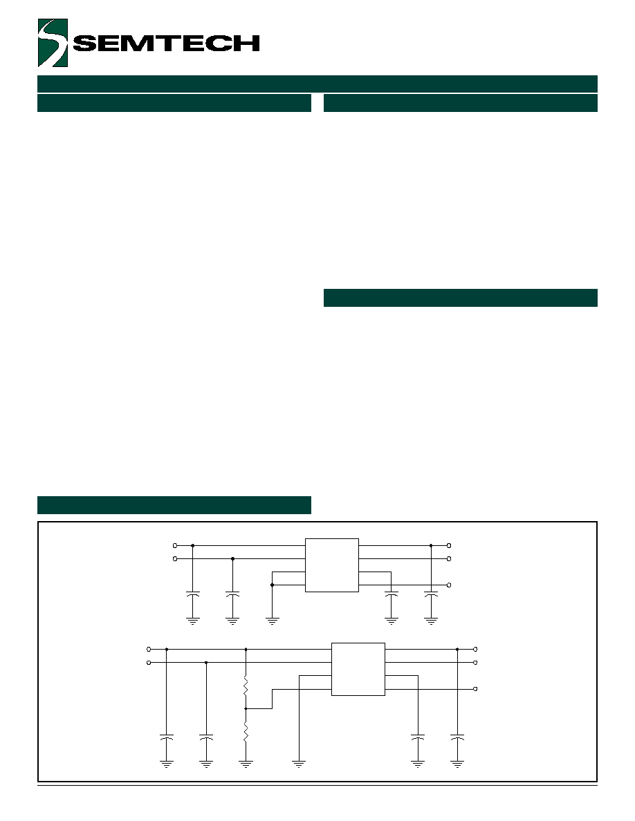
OUTPUT A: 3.0V
OUTPUT B: 3.0V
VIN
ENABLE OUTPUT A
ENABLE OUTPUT B
C3
10nF
C2
1uF
C1
1uF
C4
1uF
U1
SC1454DIMS
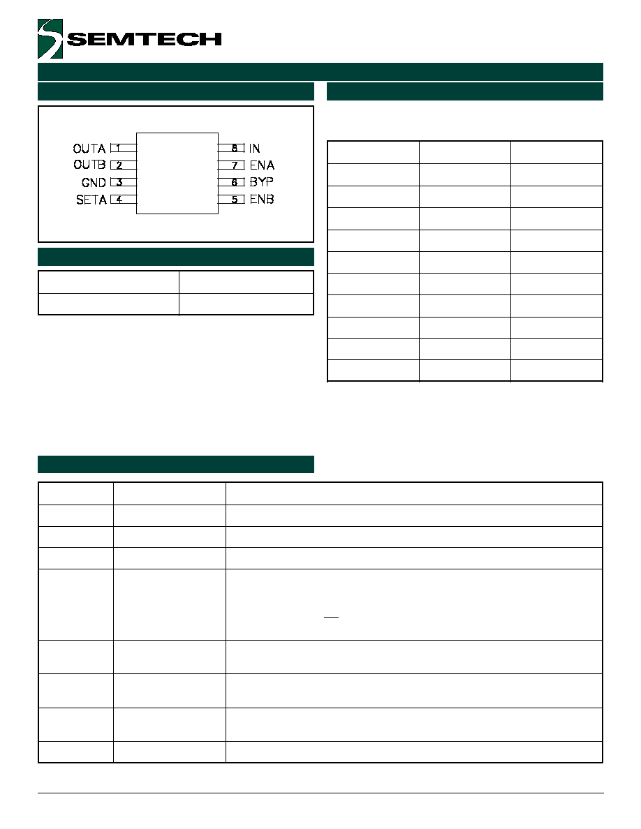
1
2
3
4
5
7
6
8
OUTA
OUTB
GND
SETA
ENB
ENA
BYP
IN
OUTPUT A: 2.5V
OUTPUT B: 2.8V
VIN
ENABLE OUTPUT A
ENABLE OUTPUT B
C3
10nF
C4
1uF
C1
1uF
C2
1uF
R1
100k
R2
100k
U1
SC1454CIMS
1
2
3
4
5
7
6
8
OUTA
OUTB
GND
SETA
ENB
ENA
BYP
IN
Description
Features
Applications
Typical Application Circuit
3
„ 2000 Semtech Corp.
www.semtech.com
SC1454
POWER MANAGEMENT
r
e
t
e
m
a
r
a
P
l
o
b
m
y
S
s
n
o
it
i
d
n
o
C
n
i
M
p
y
T
x
a
M
s
ti
n
U
).
t
n
o
C
(
B
T
U
O
,
A
T
U
O
e
g
a
tl
o
V
t
u
o
p
o
r
D
)
2
(
)
1
(
V
D
I
T
U
O
A
m
1
=
1
V
m
I
T
U
O
A
m
0
5
=
2
5
0
7
0
9
I
T
U
O
A
m
0
5
1
=
5
5
1
0
1
2
0
7
2
ti
m
i
L
t
n
e
rr
u
C
I
M
I
L
0
0
4
A
m
n
o
it
c
e
j
e
R
e
l
p
p
i
R
R
R
S
P
f
C
,
z
H
0
2
1
=
P
Y
B
F
n
0
1
=
0
6
B
d
e
s
i
o
N
e
g
a
tl
o
V
t
u
p
t
u
O
e
n
I
,
z
H
k
0
0
1
o
t
z
H
0
1
=
f
T
U
O
,
A
m
0
5
=
C
P
Y
B
C
,
F
n
0
1
=
T
U
O
F
µ
2
.
2
=
0
5
V
µ
S
M
R
I
,
z
H
M
1
o
t
z
H
0
1
=
f
T
U
O
,
A
m
0
5
=
C
P
Y
B
C
,
F
n
0
1
=
T
U
O
F
µ
2
.
2
=
5
5
B
N
E
,
A
N
E
d
l
o
h
s
e
r
h
T
t
u
p
n
I
e
l
b
a
n
E
V
H
I
6
.
1
V
V
L
I
4
.
0
t
n
e
rr
u
C
s
a
i
B
t
u
p
n
I
e
l
b
a
n
E
)
3
(
I
N
E
V
0 £ V
B
/
A
N
E
£ V
N
I
5
.
0
-
5
.
0
A
µ
P
Y
B
e
m
i
T
e
s
i
R
p
U
-t
r
a
t
S
t
r
C
P
Y
B
F
n
0
1
=
5
2
.
1
s
m
A
T
E
S
d
l
o
h
s
e
r
h
T
t
c
e
l
e
S
/
e
s
n
e
S
V
H
T
0
2
0
4
0
8
V
m
e
g
a
tl
o
V
e
c
n
e
r
e
f
e
R
A
T
E
S
V
A
T
E
S
V
N
I
I
,
V
5
.
2
=
T
U
O
A
m
1
=
%
1
-
0
5
2
.
1
%
1
+
V
A
m
0
£ I
T
U
O
£
V
5
.
2
,
A
m
0
5
1
£ V
N
I
£
V
5
.
5
%
2
-
%
2
+
t
n
e
rr
u
C
e
g
a
k
a
e
L
t
u
p
n
I
A
T
E
S
)
3
(
I
A
T
E
S
V
A
T
E
S
V
3
.
1
=
5
1
0
.
0
0
5
A
n
n
o
it
c
e
t
o
r
P
e
r
u
t
a
r
e
p
m
e
T
r
e
v
O
l
e
v
e
L
p
ir
T
h
g
i
H
T
I
H
0
5
1
C
∞
s
i
s
e
r
e
t
s
y
H
T
T
S
Y
H
0
2
C
∞
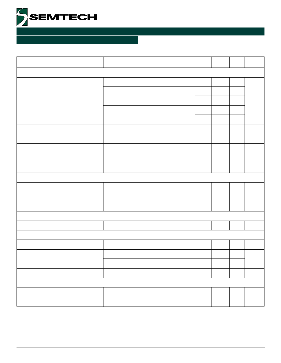
Unless specified: T
A
= 25∞C, V
IN
= V
OUT
+ 1V, I
OUTA
= I
OUTB
= 1mA, C
IN
= C
OUT
= 1.0 µF, V
ENA
= V
ENB
= V
IN
.
Values in bold apply over full operating temperature range.
Electrical Characteristics
NOTES:
(1) Low duty cycle pulse testing with Kelvin connections required.
(2) Defined as the input to output differential at which the output drops 100mV below the value measured at a
differential of 1V. Not measurable on 1.5V and 1.8V outputs due to minimum V
IN
constraints.
(3) Guaranteed by design.