 | –≠–ª–µ–∫—Ç—Ä–æ–Ω–Ω—ã–π –∫–æ–º–ø–æ–Ω–µ–Ω—Ç: SC1456 | –°–∫–∞—á–∞—Ç—å:  PDF PDF  ZIP ZIP |
Dual 150mA ULTRA LOW DROPOUT,
LOW NOISE REGULATOR
© 2000 SEMTECH CORP.
652 MITCHELL ROAD NEWBURY PARK CA 91320
SC1456
PRELIMINARY - June 15, 2000
1
DESCRIPTION
The SC1456 contains two low dropout linear regulators
that operate from a +2.5V to +6V input range and
deliver up to 150mA. PMOS pass transistors allow a
low 110µA supply current per device to remain
independent of load, making these devices ideal for
battery operated portable equipment such as cellular
phones, cordless phones and personal digital
assistants.
Each device can be powered from a separate supply
voltage or the same supply voltage for maximum
flexibility. The output voltage of each device can be
preset or adjusted with an external resistor divider.
Other features include independant low powered
shutdown, short circuit protection, thermal shutdown
protection and reverse battery protection for each
regulator. The SC1456 comes in the tiny 10 lead MSOP
package.
FEATURES
∑
Two guaranteed 150 mA outputs
∑
Designed to operate with ceramic capacitors
∑
Fixed or adjustable outputs
∑
Very small external components
∑
Low 75µV
RMS
output noise
∑
Very low supply currents
∑
Thermal overload protection
∑
Reverse battery protection
∑
Individual low power shutdown
∑
Surface mount packaging (10 pin MSOP)
∑
Full industrial temperature range
APPLICATIONS
∑
Battery Powered Systems
∑
Cellular Telephones
∑
Cordless Telephones
∑
Personal Digital Assistants
∑
Portable Instrumentation
∑
Modems
∑
PCMCIA cards
TEL:805-498-2111 FAX:805-498-3804 WEB:http://www.semtech.com
Part Number
Package
SC1456XIMSTR
(1)(2)
MSOP-10
ORDERING INFORMATION
Notes:
(1) Where X denotes voltage options - see table on page 4. Consult factory for other voltage options.
(2) Only available in tape and reel packaging. A reel contains 2500 devices.
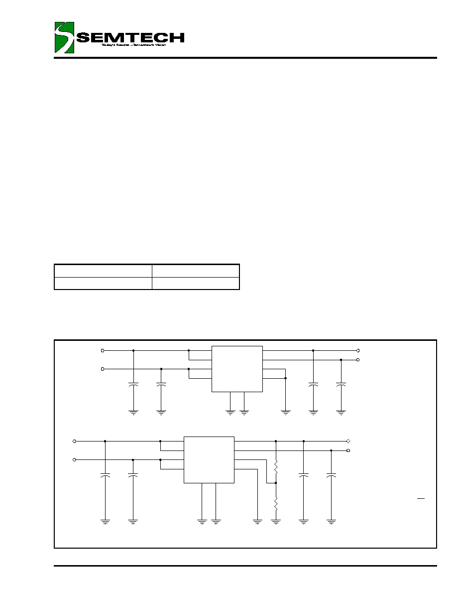
TYPICAL APPLICATIONS
VOUT1 = PRESET
VOUT2 = PRESET
VIN2
VIN1
C1
1uF
C4
1uF
C2
1uF
C3
1uF
U1
SC1456
1
2
3
4
5
6
7
8
9
10
EN1
GND
SET1
OUT2
IN2
EN2
GND
SET2
OUT1
IN1
(OR VIN1)
VOUT1 (SEE EQUATION)
VOUT2 = PRESET
VIN1
VIN2
U1
SC1456
1
2
3
4
5
6
7
8
9
10
EN1
GND
SET1
OUT2
IN2
EN2
GND
SET2
OUT1
IN1
C1
1uF
C3
2.2uF
C4
1uF
C2
1uF
R1
R2
(OR VIN1)
Output Voltages Set Internally
Output 1 Set Externally and Output 2 Set Internally
+
∑
=
k
120
2
R
2
R
1
R
1
250
.
1
V
1
OUT

Dual 150mA ULTRA LOW DROPOUT,
LOW NOISE REGULATOR
© 2000 SEMTECH CORP.
652 MITCHELL ROAD NEWBURY PARK CA 91320
SC1456
PRELIMINARY - June 15, 2000
2
ABSOLUTE MAXIMUM RATINGS
Parameter
Symbol
Maximum
Units
Input Supply Voltage
V
IN
-0.3 to +7
V
Thermal Resistance Junction to Ambient
JA
113
∞C/W
Operating Ambient Temperature Range
T
A
-40 to +85
∞C
Operating Junction Temperature Range
T
J
-40 to +125
∞C
Storage Temperature Range
T
STG
-65 to +150
∞C
Lead Temperature (Soldering) 10 seconds
T
LEAD
300
∞C
ESD Rating (Human Body Model)
ESD
1.25
kV
ELECTRICAL CHARACTERISTICS
(1)
Unless specified: V
IN
= 3.6V, V
SET
= GND, V
EN
= V
IN
, T
A
= 25∞C. Values in bold apply over full operating ambient temperature range.
Parameter
Symbol
Conditions
Min
Typ
Max
Units
IN1, IN2
Supply Voltage Range
V
IN
2.5
6.0
V
Supply Current
I
Q
I
OUT
= 0mA
90
130
µA
160
50mA
I
OUT
150mA
110
160
µA
200
V
EN
= 0V
0.0001
1
µA
2
OUT1, OUT2
Output Voltage
(2)
V
OUT
I
OUT
= 1mA
-2.0%
V
OUT
+2.0%
V
1mA
I
OUT
150mA, V
OUT
+1V
V
IN
5.5V
-3.5%
+3.5%
Line Regulation
(2)
REG
(LINE)
2.5V
V
IN
5.5V, V
SET
= V
OUT
, I
OUT
= 1mA
5
10
mV
12
Load Regulation
(2)
REG
(LOAD)
I
OUT
= 0mA to 50mA
-10
-15
mV
-20
I
OUT
= 0mA to 100mA
-15
-20
mV
-25
I
OUT
= 0mA to 50mA, V
SET
= V
OUT
-2.5
-7.5
mV
-15.0
I
OUT
= 0mA to 100mA, V
SET
= V
OUT
-5
-15
mV
-30

Dual 150mA ULTRA LOW DROPOUT,
LOW NOISE REGULATOR
© 2000 SEMTECH CORP.
652 MITCHELL ROAD NEWBURY PARK CA 91320
SC1456
PRELIMINARY - June 15, 2000
3
ELECTRICAL CHARACTERISTICS
(1)
(Cont.)
Unless specified: V
IN
= 3.6V, V
SET
= GND, V
EN
= V
IN
, T
A
= 25∞C. Values in bold apply over full operating ambient temperature range.
Parameter
Symbol
Conditions
Min
Typ
Max
Units
OUT1, OUT2 (Cont.)
Dropout Voltage
(2)(3)
V
D
I
OUT
= 1mA
1.1
mV
I
OUT
= 50mA
55
90
mV
120
I
OUT
= 100mA
110
180
mV
240
Current Limit
I
LIM
150
240
350
mA
Output Voltage Noise
e
n
10Hz to 99kHz, I
OUT
= 50mA, C
OUT
= 1µF
90
µV
RMS
C
OUT
= 100µF
75
Power Supply Rejection Ratio
PSRR
f = 120Hz
55
dB
EN1, EN2
EN Input Threshold
V
IH
1.8
V
V
IL
0.4
EN Input Bias Current
(4)
I
EN
V
EN
= V
IN
0
100
nA
200
SET1, SET2
Sense/Select Threshold
V
TH
20
55
80
mV
SET Reference Voltage
(2)
V
SET
I
OUT
= 1mA
1.225 1.250 1.275
V
1mA
I
OUT
150mA, 2.5V
V
IN
5.5V
1.206
1.294
SET Input Leakage Current
(4)
I
SET
V
SET
= 1.3V
0.015 2.500
nA
5.000
OVER TEMPERATURE PROTECTION
High Trip Level
T
HI
170
∞C
Hysteresis
T
HYST
10
∞C
NOTE:
(1) This device is ESD sensitive. Use of standard ESD handling precautions is required.
(2) Low duty cycle pulse testing with Kelvin connections required.
(3) Defined as the input to output differential at which the output voltage drops 100mV below the value measured
at a differential of 2V.
(4) Guaranteed by design.

Dual 150mA ULTRA LOW DROPOUT,
LOW NOISE REGULATOR
© 2000 SEMTECH CORP.
652 MITCHELL ROAD NEWBURY PARK CA 91320
SC1456
PRELIMINARY - June 15, 2000
4
BLOCK DIAGRAM
PIN CONFIGURATION
Top View
MSOP-10
PIN DESCRIPTIONS
Pin #
Pin Name Description
1
EN1
Active high enable pin for device 1. Connect to VIN1 if not being used.
2
GND
Ground pin. Can be used for heatsinking if needed. Electrically connected to pin 7.
3
SET1
Connecting this pin to ground results in the internally preset value for V
OUT1
. Connecting to an
external resistor divider changes V
OUT1
to:
4
OUT2
Regulator output for device 2, sourcing up to 150mA
5
IN2
Supply input pin for device 2.
6
EN2
Active high enable pin for device 2. Connect to VIN2 if not being used.
7
GND
Ground pin. Can be used for heatsinking if needed. Electrically connected to pin 2.
8
SET2
Connecting this pin to ground results in the internally preset value for V
OUT2
. Connecting to an
external resistor divider changes V
OUT2
to:
9
OUT1
Regulator output for device 1, sourcing up to 150mA
10
IN1
Supply input pin for device 1.
+
∑
=
2
R
1
R
1
250
.
1
V
1
OUT
+
∑
=
2
R
1
R
1
250
.
1
V
2
OUT
VOLTAGE OPTIONS
Replace X in the part number (SC1456XIMS) by the letter shown
below for the corresponding voltage option:
X
V
OUTA
(V)
V
OUTB
(V)
A
2.5
2.5
B
2.8
2.8
C
3.0
3.0
D
3.3
3.3
Dual 150mA ULTRA LOW DROPOUT,
LOW NOISE REGULATOR
© 2000 SEMTECH CORP.
652 MITCHELL ROAD NEWBURY PARK CA 91320
SC1456
PRELIMINARY - June 15, 2000
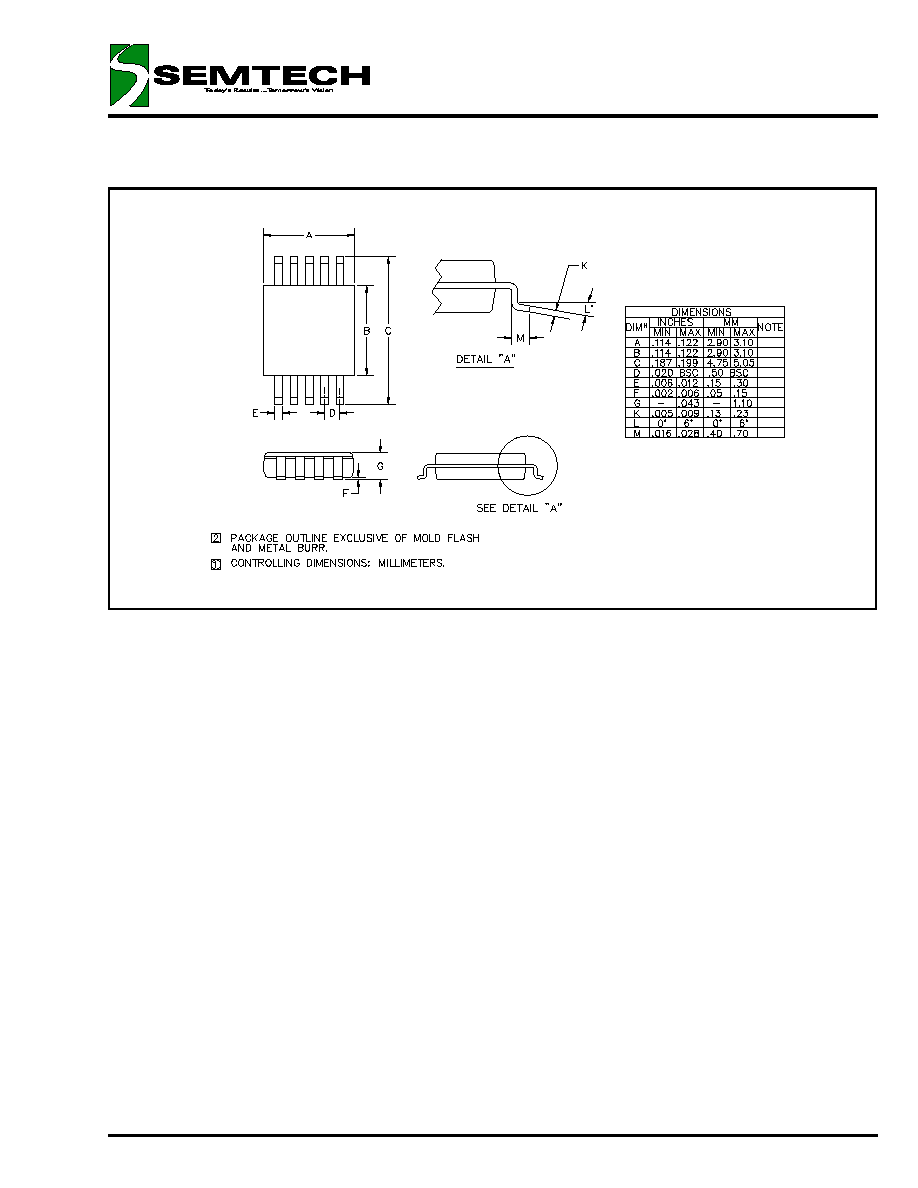
5
DEVICE OUTLINE - MSOP-10
ECN 00-1167