 | –≠–ª–µ–∫—Ç—Ä–æ–Ω–Ω—ã–π –∫–æ–º–ø–æ–Ω–µ–Ω—Ç: SC1532 | –°–∫–∞—á–∞—Ç—å:  PDF PDF  ZIP ZIP |
© 2000 SEMTECH CORP.
652 MITCHELL ROAD NEWBURY PARK CA 91320
400mA SmartLDO
TM
with Internal Pass
MOSFET
SC1532
January 3, 2000
1
TEL:805-498-2111 FAX:805-498-3804 WEB:http://www.semtech.com
DESCRIPTION
Intended for applications such as Power Managed PCI,
the SC1532 is designed to maintain a glitch-free 3.3V
output when at least one of two inputs, 5V (VIN1) and
3.3V (VIN2), is present.
The SC1532 combines a 5V to 3.3V linear regulator
with an integral 3.3V bypass switch, along with logic
and detection circuitry to control which supply provides
the power for the output.
Whenever VIN1 exceeds a predetermined threshold
value, the internal 3.3V PMOS linear regulator is en-
abled, and the internal pass NMOS is turned off.
When VIN1 falls below a lower threshold value, the
NMOS pass device is turned on and the PMOS linear
regulator is turned off. This ensures an uninterrupted
3.3V output even if VIN1 falls out of specification.
When both supplies are simultaneously available, the
PMOS linear regulator will be turned on, and the
NMOS pass will be turned off, thus preferentially sup-
plying the output from the 5V supply.
The internal 5V detector has its upper threshold (for
VIN1 rising) set to 4.18V (typical) while the lower
threshold (for VIN falling) is at 4.1V (typical) giving a
hysteresis of approximately 80mV.
The SC1532 is available in the popular SO-8 surface
mount package.
FEATURES
∑
Glitch-free transition between input sources
∑
Internal logic selects input source
∑
5V detector with hysteresis
∑
1% regulated output voltage accuracy
∑
400mA load current capability
APPLICATIONS
∑
Desktop Computers
∑
Network Interface Cards (NICs)
∑
PCMCIA/PCI Interface Cards
∑
Peripheral Cards
ORDERING INFORMATION
Part Number
(1)
Package
SC1532CS
SO-8
Note:
(1) Add suffix `TR' for tape and reel packaging.
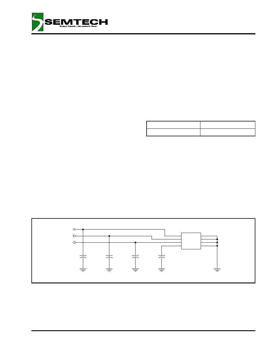
TYPICAL APPLICATION CIRCUIT
3.3VAUX IN
5V IN
3.3V OUT
U1
SC1532
1
2
3
4
5
6
7
8
VIN2
VIN1
VO
CP
GND
GND
GND
GND
C4
1nF
C1
4.7uF
C2
4.7uF
C3
4.7uF
NOTES:
(1) Ceramic capacitors are recommended - see Applications Information for further details.
(2) Output capacitor C3 needs to be 1.0uF or greater for stability. Additional capacitance (tantalum or ceramic) will
improve overall performance.

© 2000 SEMTECH CORP.
652 MITCHELL ROAD NEWBURY PARK CA 91320
400mA SmartLDO
TM
with Internal Pass
MOSFET
SC1532
January 3, 2000
2
NOTE:
(1) 1 inch square of 1/16" FR-4, double sided, 1 oz. minimum copper weight.
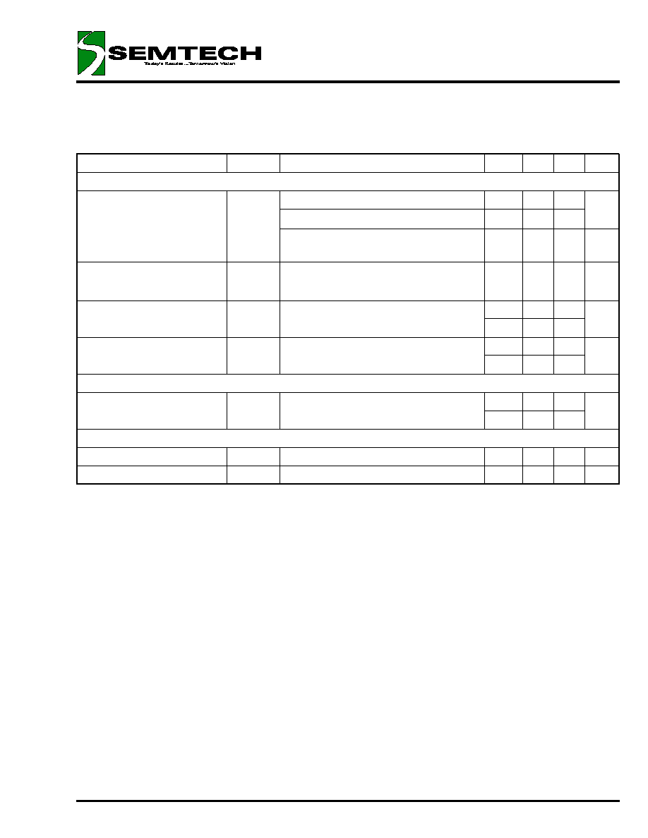
ABSOLUTE MAXIMUM RATINGS
Parameter
Symbol
Maximum
Units
Input Supply Voltages
VIN1, VIN2
-0.5 to +7
V
Charge Pump Capacitor Pin Voltage
CP
-0.5 to +16
V
Output Current
I
O
400
mA
Operating Ambient Temperature Range
T
A
-5 to +70
∞C
Operating Junction Temperature Range
T
J
-5 to +125
∞C
Storage Temperature Range
T
STG
-65 to +150
∞C
Lead Temperature (Soldering) 10 Sec
T
LEAD
300
∞C
Thermal Impedance Junction to Ambient
(1)
JA
65
∞C/W
ESD Rating (Human Body Model)
ESD
4
kV
ELECTRICAL CHARACTERISTICS
Unless specified, T
A
= 25∞C, VIN1 = 5V, VIN2 = 3.3V, I
O
= 400mA, CIN1 = 4.7uF, CIN2 = 4.7uF, C
O
= 4.7uF, Cp=1nF.
Values in bold apply over full operating temperature range.
Parameter
Symbol
Test Conditions
MIN
TYP MAX Units
VIN1
Supply Voltage
VIN1
VIN2 = 0V
4.3
5.0
5.5
V
Quiescent Current
I
Q1
VIN1 = 5V, 0V
VIN2
3.6V, I
O
= 0mA
2.0
3.0
mA
4.0
Reverse Leakage From VIN2
(1)
I
VIN1
VIN1 = 0V, VIN2 = 3.6V, I
O
= 0mA
0
1
µA
VIN2
Supply Voltage
VIN2
3.0
3.3
3.6
V
Quiescent Current
I
Q2
VIN2 = 3.3V, 0V
VIN1
5.5V, I
O
= 0mA
650 1300
µA
2000
Reverse Leakage From VIN1
(1)
I
VIN2
VIN1 = 5.5V, VIN2 = 0V, I
O
= 0mA
0
1
µA
5V Detect
(1)(2)
Low Threshold Voltage
V
TH(LO)
VIN1 Falling, I
O
= 20mA
3.90
4.10
V
Hysteresis
V
HYST
I
O
= 20mA
60
80
150
mV
High Threshold Voltage
V
TH(HI)
VIN1 Rising, I
O
= 20mA
4.18 4.30
V
© 2000 SEMTECH CORP.
652 MITCHELL ROAD NEWBURY PARK CA 91320
400mA SmartLDO
TM
with Internal Pass
MOSFET
SC1532
January 3, 2000
3
NOTES:
(1) Guaranteed by design.
(2) Recommended source impedance for 5V supply:
0.125
. This will ensure clean transitions between supplies
with no "chattering" (see Applications Information).
(3) Refer to block diagram.
ELECTRICAL CHARACTERISTICS (Cont.)
Unless specified, T
A
= 25∞C, VIN1 = 5V, VIN2 = 3.3V, I
O
= 400mA, CIN1 = 4.7uF, CIN2 = 4.7uF, C
O
= 4.7uF, Cp=1nF.
Values in bold apply over full operating temperature range.
Parameter
Symbol
Test Conditions
MIN
TYP MAX Units
VO
LDO Voltage Accuracy
VO
I
O
= 20mA
-1
+1
%
4.3V
VIN1
5.5V, 0mA
I
O
400mA
(1)
-2
+2
3.90V
VIN1
4.3V, VIN2 = 3.3V,
0mA
I
O
400mA
(1)
3.000
V
VIN2 Pass Device On Resis-
R
DS(ON)
VIN1 < 3.9V, 0mA
I
O
400mA
360
500
m
tance
(Aux. NMOS)
(1)(3)
Line Regulation
REG
(LINE)
VIN1 = 4.3V to 5.5V
0.3
0.6
%
0.7
Load Regulation
REG
(LOAD)
I
O
= 20mA to 400mA
0.3
0.6
%
0.7
Current Limit (LDO)
Output Current
I
LIM
VIN1 = 5V, VIN2 = 0V, VO = 0V
600
975 1200
mA
1400
Over Temperature Protection
High Trip Level
T
HI
VIN1=5V
175
∫C
Hysteresis
T
HYS
VIN1=5V
10
∫C
© 2000 SEMTECH CORP.
652 MITCHELL ROAD NEWBURY PARK CA 91320
400mA SmartLDO
TM
with Internal Pass
MOSFET
SC1532
January 3, 2000
4
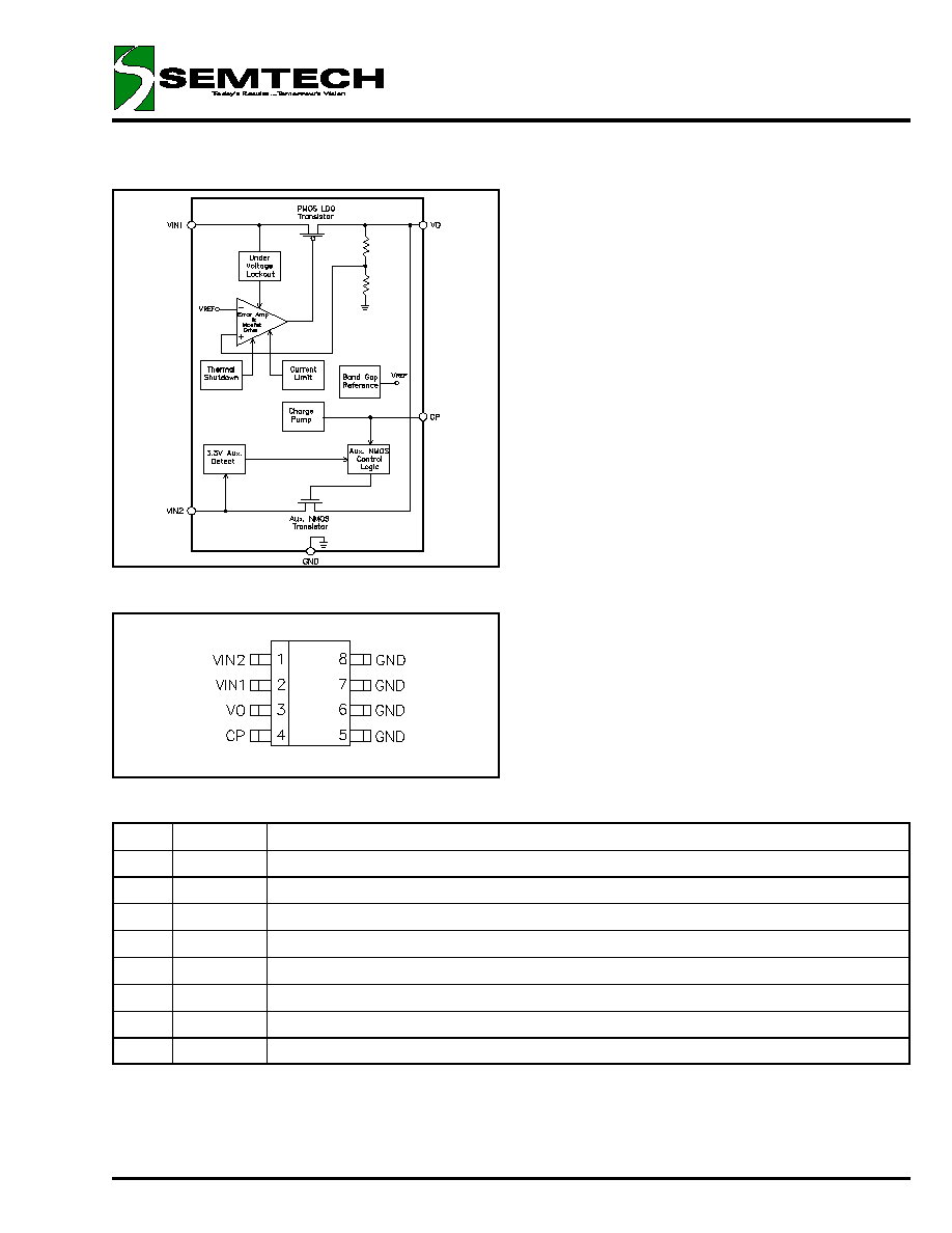
Top View
(SO-8)
PIN DESCRIPTIONS
Pin
Pin Name
Pin Function
1
VIN2
Secondary input supply, nominally 3.3V.
2
VIN1
Main input supply for the IC, nominally 5V.
3
VO
3.3V out.
4
CP
Charge pump capacitor connection.
5
GND
Ground pin.
6
GND
Ground pin.
7
GND
Ground pin.
8
GND
Ground pin.
PIN CONFIGURATION
BLOCK DIAGRAM
© 2000 SEMTECH CORP.
652 MITCHELL ROAD NEWBURY PARK CA 91320
400mA SmartLDO
TM
with Internal Pass
MOSFET
SC1532
January 3, 2000
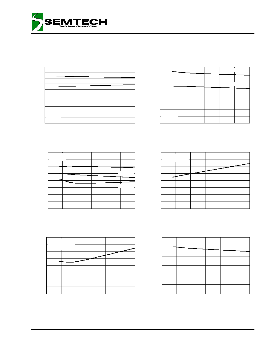
5
0.00
0.05
0.10
0.15
0.20
0.25
0.30
0.35
0.40
-25
0
25
50
75
100
125
T
J
(∞C)
REG
(LOAD)
(%)
VIN1 = 5V
VIN2 = 3.3V
I
O
= 20mA to 400mA
0.00
0.05
0.10
0.15
0.20
0.25
0.30
0.35
0.40
-25
0
25
50
75
100
125
T
J
(∞C)
REG
(LINE)
(%)
VIN1 = 4.3V to 5.5V
I
O
= 400mA
0.0
0.2
0.4
0.6
0.8
1.0
1.2
1.4
1.6
1.8
2.0
-25
0
25
50
75
100
125
T
J
(∞C)
I
Q1
(mA)
VIN1 = 5V
I
O
= 0mA
VIN2 = 3.6V
VIN2 = 0V
TYPICAL CHARACTERISTICS
Quiescent Current (I
Q1
) vs.
Junction Temperature vs. VIN2
0
100
200
300
400
500
600
700
800
-25
0
25
50
75
100
125
T
J
(∞C)
I
Q2
(µA)
VIN1 = 0V
VIN1 = 5.5V
VIN2 = 3.3V
I
O
= 0mA
Quiescent Current (I
Q2
) vs.
Junction Temperature vs. VIN1
LDO Line Regulation vs.
Junction Temperature
LDO Load Regulation vs.
Junction Temperature
3.270
3.275
3.280
3.285
3.290
3.295
3.300
3.305
3.310
-25
0
25
50
75
100
125
T
J
(∞C)
V
O
(V)
I
O
= 0mA
I
O
= 200mA
I
O
= 400mA
VIN1 = 5V
VIN2 = 3.3V
LDO Output Voltage vs. Junction
Temperature vs. Output Current
0
200
400
600
800
1000
1200
-25
0
25
50
75
100
125
T
J
(∞C)
I
LIM
(mA)
VIN1 = 5V
VIN2 = 0V
VO = 0V
LDO Current Limit vs.
Junction Temperature