 | –≠–ª–µ–∫—Ç—Ä–æ–Ω–Ω—ã–π –∫–æ–º–ø–æ–Ω–µ–Ω—Ç: SC1563 | –°–∫–∞—á–∞—Ç—å:  PDF PDF  ZIP ZIP |

© 2000 SEMTECH CORP.
652 MITCHELL ROAD NEWBURY PARK CA 91320
VERY LOW DROPOUT, LOW
QUIESCENT 500mA REGULATOR
SC1563
PRELIMINARY - September 11, 2000
1
FEATURES
∑
=
450mV dropout @ 500mA
∑
=
Designed to operate with ceramic capacitors
∑
=
Adjustable output from 1.200V to 3.3V
∑
=
Multiple output voltage options (all parts also
adjustable externally using resistors)
∑
=
Over current and over temperature protection
∑
=
Enable pin
∑
=
1µA quiescent current in shutdown
∑
=
Low reverse leakage (output to input)
∑
=
Full industrial temperature range
DESCRIPTION
The SC1563 is a high performance positive voltage
regulator designed for use in applications requiring
very low dropout voltage at up to 500 milliamps. Since
it has superior dropout characteristics compared to
regular LDOs, it can be used to supply 2.5V on
motherboards or 2.8V on peripheral cards from the
3.3V supply with no heatsink. Additionally, the SC1563
has a shutdown pin, to further reduce power
dissipation while shut down. The SC1563 provides
excellent regulation over variations in line, load and
temperature.
The SC1563 is available as a five terminal fixed or
adjustable output voltage device with enable. The
device is available in a 5-pin SOT-23 package and an
8-pin MSOP package for higher power dissipation/
lower junction temperature.
APPLICATIONS
∑
=
Battery powered systems
∑
=
Motherboards
∑
=
Peripheral cards
∑
=
PCMCIA cards
DEVICE
(1)(2)(3)
PACKAGE
SC1563ISK-X.XTR
SOT-23-5L
SC1563IMS-X.XTR
MSOP-8
ORDERING INFORMATION
Notes:
(1) Where -X.X denotes voltage options. Available
voltages are: 1.8V, 2.5V, 2.8V, 3.0V, 3.1V and 3.3V.
(2) Output voltage can be adjusted using external re-
sistors, see Pin Description.
(3) Only available in tape and reel packaging. A reel
contains 2500 devices (MSOP-8) or 3000 devices
(SOT-23-5L).
TEL:805-498-2111 FAX:805-498-3804 WEB:http://www.semtech.com
TYPICAL APPLICATION
Internally Preset Output Voltage
Externally Set Output Voltage
Volts
R2
R2)
(R1
1.200
VO
+
=
VIN
SHDN
VO (X.XV)
VIN
SHDN
VO
U1
SC1563ISK-X.X
1
2
3
4
5
SHDN GND ADJ
VO
VIN
C1
C2
U1
SC1563ISK-X.X
1
2
3
4
5
SHDN GND ADJ
VO
VIN
C1
C2
R1
R2
© 2000 SEMTECH CORP.
652 MITCHELL ROAD NEWBURY PARK CA 91320
VERY LOW DROPOUT, LOW
QUIESCENT 500mA REGULATOR
SC1563
PRELIMINARY - September 11, 2000
2
ABSOLUTE MAXIMUM RATINGS
Parameter
Symbol
Maximum
Units
Input Voltage
V
IN
5.5
V
Power Dissipation
P
D
Internally Limited
W
Thermal Resistance Junction to Ambient
MSOP-8
(1)
MSOP-8
(2)
SOT-23-5L
(1)
JA
206
95
256
∞C/W
Thermal Resistance Junction to Case
MSOP-8
SOT-23-5L
JC
39
81
∞C/W
Operating Ambient Temperature Range
T
A
-40 to+85
∞C
Operating Junction Temperature Range
T
J
-40 to 150
∞C
Storage Temperature Range
T
STG
-65 to 150
∞C
Lead Temperature (Soldering) 10 Sec.
T
LEAD
300
∞C
ESD Rating
ESD
2
kV
ELECTRICAL CHARACTERISTICS
Unless specified: V
SHDN
= 0V
Adjustable Option (V
ADJ
> V
TH(ADJ)
): V
IN
= 2.2 to 5.5V and I
O
= 10µA to 500mA
Fixed Options (V
ADJ
= GND): V
IN
= (V
O
+ 0.7V) to 5.5V and I
O
= 0A to 500mA
Values in bold apply over the full operating temperature range.
Parameter
Symbol
Test Conditions
Min
Typ
Max
Units
VIN
Supply Voltage Range
VIN
2.2
5.5
V
Quiescent Current
I
Q
V
IN
= 3.3V
100
150
µA
V
IN
= 5.5V, V
SHDN
= Open
0.5
2
µA
VO
Output Voltage
(1)
V
O
V
IN
= V
O
+ 0.7V, I
O
= 10mA
0.99V
O
V
O
1.01V
O
V
(Internal Fixed Voltage)
0.98V
O
V
O
1.02V
O
Line Regulation
(1)
REG
(LINE)
V
IN
= (V
O
+ 0.25V) to 5.5V, I
OUT
= 10mA
0.035
0.3
%
Load Regulation
(1)
REG
(LOAD)
V
IN
= V
O
+ 0.7V
0.2
0.4
%
Notes:
(1) Minimum pad size.
(2) 1 square inch of FR-4, double sided, 1oz. minimum copper weight.
© 2000 SEMTECH CORP.
652 MITCHELL ROAD NEWBURY PARK CA 91320
VERY LOW DROPOUT, LOW
QUIESCENT 500mA REGULATOR
SC1563
PRELIMINARY - September 11, 2000
3
NOTES:
(1) Low duty cycle pulse testing with Kelvin connections required.
(2) Defined as the input to output differential at which the output voltage drops to 1% below the value measured at
a differential of 0.7V.
(3) Required to maintain regulation. Voltage set resistors R1 and R2 are usually utilized to meet this requirement.
Adjustable versions only.
(4) Guaranteed by design.
(5) When V
ADJ
exceeds this threshold, the "Sense Select" switch disconnects the internal feedback chain from the
error amplifier and connects V
ADJ
instead.
ELECTRICAL CHARACTERISTICS (Cont.)
Unless specified: V
SHDN
= 0V
Adjustable Option (V
ADJ
> V
TH(ADJ)
): V
IN
= 2.2 to 5.5V and I
O
= 10µA to 500mA
Fixed Options (V
ADJ
= GND): V
IN
= (V
O
+ 0.7V) to 5.5V and I
O
= 0A to 500mA
Values in bold apply over the full operating temperature range.
Parameter
Symbol
Test Conditions
Min
Typ
Max
Units
VO (Cont.)
Dropout Voltage
(2)
V
D
I
LOAD
= 2mA
1
5
mV
10
I
LOAD
= 100mA
75
100
mV
150
I
LOAD
= 250mA
200
300
mV
400
I
LOAD
= 500mA
450
550
mV
700
Minimum Load Current
(3)
I
O
V
IN
= V
O
+ 0.7V
1
10
µA
Current Limit
I
CL
0.50
1.00
A
ADJ
Reference Voltage
(1)
V
REF
V
IN
= 2.2V, V
ADJ
= V
OUT
, I
O
= 10mA
1.188
1.200
1.212
V
1.176
1.224
Adjust Pin Current
(4)
I
ADJ
V
ADJ
= V
REF
50
100
nA
Adjust Pin Threshold
(5)
V
TH(ADJ)
0.10
0.20
0.40
V
SHDN
Shutdown Pin Current
I
SHDN
V
SHDN
= 0V, V
IN
= 3.3V
1
10
µA
Shutdown Pin Threshold
V
IH
V
IN
= 3.3V
1.8
V
V
IL
V
IN
= 3.3V
0.4
OVER TEMPERATURE PROTECTION
High Trip Level
T
HI
165
∞C
Hysteresis
T
HYST
10
∞C
© 2000 SEMTECH CORP.
652 MITCHELL ROAD NEWBURY PARK CA 91320
VERY LOW DROPOUT, LOW
QUIESCENT 500mA REGULATOR
SC1563
PRELIMINARY - September 11, 2000
4
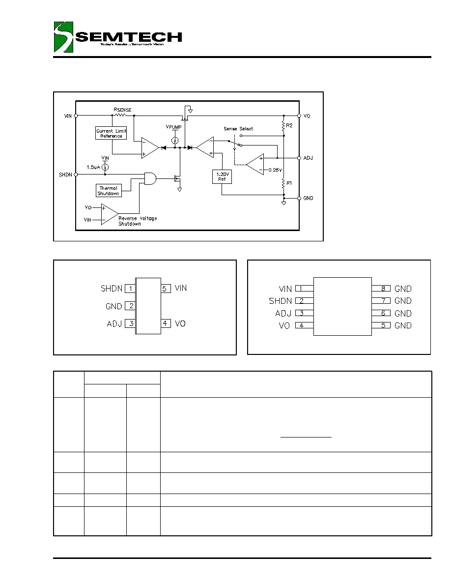
PIN DESCRIPTION
Pin
Pin Number
Pin Function
Name
SOT-23-5L MSOP-8
ADJ
3
3
This pin, when grounded, sets the output voltage to that set by the internal feed-
back resistors. If external feedback resistors are used, the output voltage will be
(See Application Circuit):
GND
2
5-8
Reference ground. Connect all MSOP-8 GND pins. These pins may be used for
heatsinking purposes.
VIN
5
1
Input voltage. For regulation at full load, the input to this pin must be between (VO
+ 0.7V) to 5.5V. Minimum VIN = 2.2V.
VO
4
4
This pin is the power output of this device.
SHDN
1
2
Shutdown Input. Leaving this pin open turns the regulator off, reducing the quies-
cent current to a fraction of its operating value (typically <100nA). The device will
be enabled if this pin is pulled below 0.4V. Connect to GND if not being used.
Volts
R2
R2)
(R1
1.200
VO
+
=
BLOCK DIAGRAM
PIN CONFIGURATIONS
Top View
SOT-23-5L
Top View
MSOP-8

© 2000 SEMTECH CORP.
652 MITCHELL ROAD NEWBURY PARK CA 91320
VERY LOW DROPOUT, LOW
QUIESCENT 500mA REGULATOR
SC1563
PRELIMINARY - September 11, 2000
5
TYPICAL APPLICATION (Externally Set Output Voltage)
(1)(2)
Volts
R2
R2)
(R1
1.200
VO
+
=
Notes:
(1) Maximum VO setpoint is 3.3V.
(2) This device is designed to operate with ceramic input and output capacitors.
TYPICAL APPLICATIONS (Internally Set Output Voltage)
(2)
VIN
SHDN
VO (X.XV)
U1
SC1563IS-X.X
1
2
3
4
5
SHDN GND ADJ
VO
VIN
C1
1uF
C2
10uF
VIN
SHDN
VO
U1
SC1563IS-X.X
1
2
3
4
5
SHDNGND ADJ
VO
VIN
C1
1uF
C2
10uF
R1
R2
VIN
VO (X.XV)
SHDN
U1 SC1563IMS-X.X
1
2
3
4
5
6
7
8
VIN
SHDN
ADJ
VO
GND
GND
GND
GND
C1
1uF
C2
10uF