SC1563 data sheet
POWER MANAGEMENT
1
www.semtech.com
SC1563
Very Low Dropout, Low
Quiescent 500mA Regulator
Revision 4, October 2002
The SC1563 is a high performance positive voltage
regulator designed for use in applications requiring very
low dropout voltage at up to 500mA. Since it has supe-
rior dropout characteristics compared to regular LDOs, it
can be used to supply 2.5V on motherboards or 2.8V on
peripheral cards from the 3.3V supply with no heatsink.
Additionally, the SC1563 has a shutdown pin to further
reduce power dissipation while shut down. The SC1563
provides excellent regulation over variations in line, load
and temperature.
A wide range of fixed output voltage options are
available. In addition, the output voltage of every device
can be adjusted between 1.2V and 4.8V using external
resistors. The SC1563 comes in both 5-pin
SOT-23 and 8-pin MSOP packages to allow the user to
select a package suitable for their spacing and heat
dissipation needs.
350mV dropout @ 500mA
Designed to operate with ceramic capacitors
Adjustable output from 1.2V to 4.8V
Multiple output voltage options (all parts also
adjustable externally using resistors)
Over current and over temperature protection
2µA quiescent current in shutdown
No minimum load current requirement
Low reverse leakage (output to input)
Full industrial temperature range
SOT-23-5 and MSOP-8 surface mount packages
Personal Digital Assistants
Battery powered systems
Motherboards
Peripheral cards
PCMCIA cards
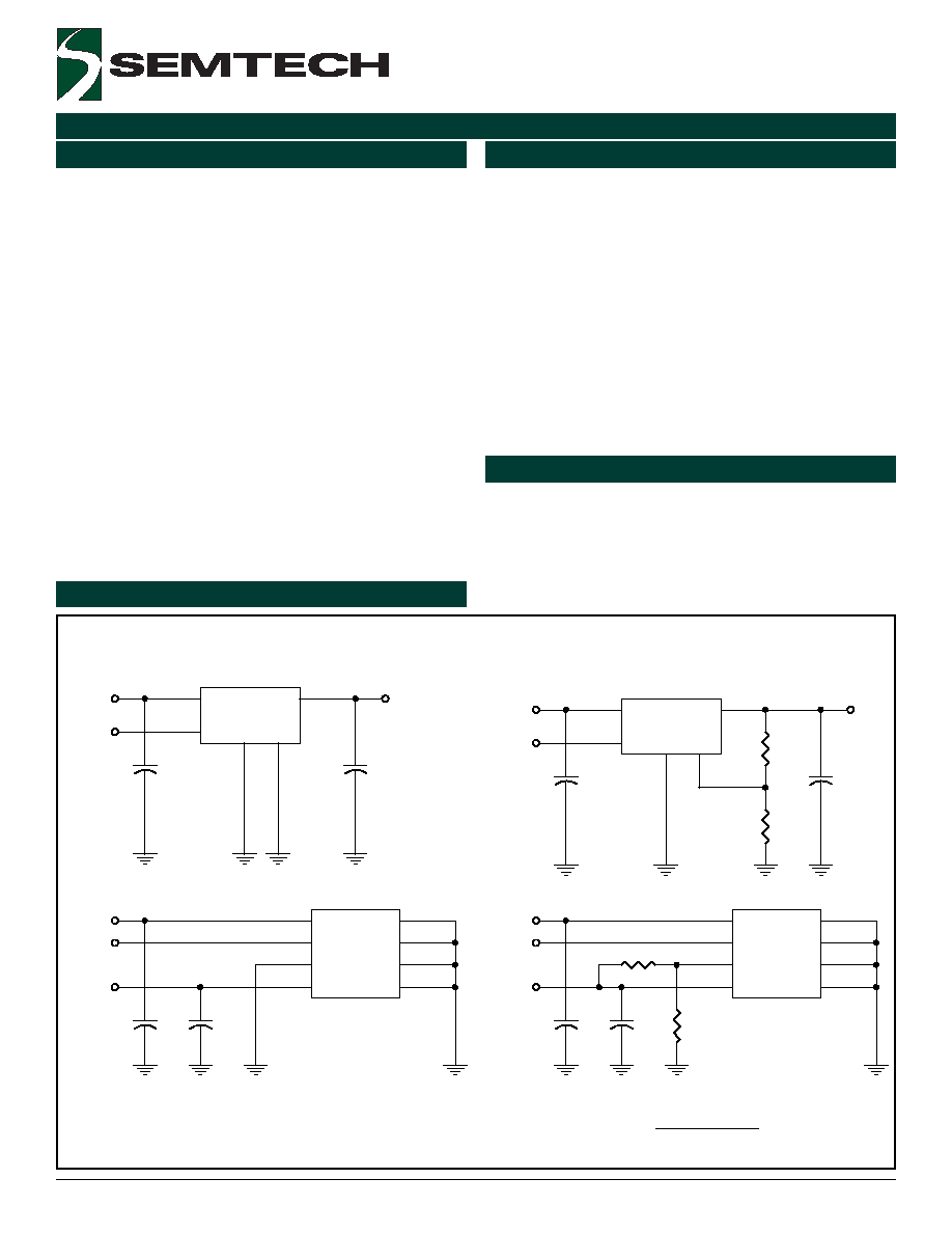
Internally Preset Output Voltage
Externally Set Output Voltage
U1
SC1563IS-X.X
1
2
3
4
5
SHDN GND ADJ
OUT
IN
C2
R1
R2
C2
U1 SC1563IMS-X.X
1
2
3
4
5
6
7
8
IN
SHDN
ADJ
OUT
GND
GND
GND
GND
R2
C1
VIN
U1 SC1563IMS-X.X
1
2
3
4
5
6
7
8
IN
SHDN
ADJ
OUT
GND
GND
GND
GND
VO (X.XV)
VO
SHDN
SHDN
VO (X.XV)
C1
C2
VIN
C1
SHDN
R1
C2
VO
VIN
C1
VIN
SHDN
U1
SC1563IS-X.X
1
2
3
4
5
SHDN GND ADJ
OUT
IN
Volts
R2
R2)
(R1
1.200
V
OUT
+
=
Description
Features
Applications
Typical Application Circuits
2
2002 Semtech Corp.
www.semtech.com
POWER MANAGEMENT
SC1563
r
e
t
e
m
a
r
a
P
l
o
b
m
y
S
s
n
o
i
t
i
d
n
o
C
n
i
M
p
y
T
x
a
M
s
t
i
n
U
N
I
e
g
n
a
R
e
g
a
tl
o
V
y
l
p
p
u
S
V
N
I
2
.
2
5
.
6
V
t
n
e
r
r
u
C
t
n
e
c
s
e
i
u
Q
I
Q
V
N
I
V
3
.
3
=
5
8
0
5
1
A
µ
V
N
I
V
,
V
5
.
6
=
N
D
H
S
n
e
p
O
=
1
0
.
0
0
0
.
2
A
µ
T
U
O
e
g
a
tl
o
V
t
u
p
t
u
O
)
1
(
V
T
U
O
V
N
I
V
=
T
U
O
I
,
V
7
.
0
+
T
U
O
A
m
0
1
=
%
1
-
V
T
U
O
%
1
+
V
)
e
g
a
tl
o
V
d
e
x
i
F
l
a
n
r
e
t
n
I
(
%
2
-
%
2
+
n
o
it
a
l
u
g
e
R
e
n
i
L
)
1
(
G
E
R
)
E
N
I
L
(
V
N
I
V
(
=
T
U
O
I
,
V
5
.
5
o
t
)
V
5
2
.
0
+
T
U
O
A
m
0
1
=
1
.
0
4
.
0
%
n
o
it
a
l
u
g
e
R
d
a
o
L
)
1
(
G
E
R
)
D
A
O
L
(
V
N
I
V
=
T
U
O
V
7
.
0
+
5
1
.
0
0
4
.
0
%
Unless specified: V
SHDN
= 0V, Adjustable mode (V
ADJ
> V
TH(ADJ)
): V
IN
= 2.2V to 5.5V and I
OUT
= 0A to 500mA,
Fixed mode (V
ADJ
= GND): V
IN
= (V
OUT
+ 0.7V) to 5.5V and I
OUT
= 0A to 500mA. Values in bold apply over full operating temperature range.
r
e
t
e
m
a
r
a
P
l
o
b
m
y
S
m
u
m
i
x
a
M
s
t
i
n
U
e
g
a
tl
o
V
t
u
p
n
I
V
N
I
7
o
t
3
.
0
-
V
e
g
a
tl
o
V
n
w
o
d
t
u
h
S
V
N
D
H
S
V
o
t
3
.
0
-
N
I
V
n
o
it
a
p
i
s
s
i
D
r
e
w
o
P
P
D
d
e
ti
m
i
L
y
ll
a
n
r
e
t
n
I
W
t
n
e
i
b
m
A
o
t
n
o
it
c
n
u
J
e
c
n
a
t
s
i
s
e
R
l
a
m
r
e
h
T
8
-
P
O
S
M
)
1
(
8
-
P
O
S
M
)
2
(
5
-
3
2
-
T
O
S
)
1
(
A
J
6
0
2
5
9
6
5
2
W
/
C
°
e
s
a
C
o
t
n
o
it
c
n
u
J
e
c
n
a
t
s
i
s
e
R
l
a
m
r
e
h
T
8
-
P
O
S
M
5
-
3
2
-
T
O
S
C
J
9
3
1
8
W
/
C
°
g
n
it
a
r
e
p
O
t
n
e
i
b
m
A
e
g
n
a
R
e
r
u
t
a
r
e
p
m
e
T
T
A
5
8
o
t
0
4
-
C
°
g
n
it
a
r
e
p
O
n
o
it
c
n
u
J
e
g
n
a
R
e
r
u
t
a
r
e
p
m
e
T
T
J
4
-
0
5
1
o
t
0
C
°
e
g
n
a
R
e
r
u
t
a
r
e
p
m
e
T
e
g
a
r
o
t
S
T
G
T
S
0
5
1
o
t
5
6
-
C
°
c
e
s
0
1
)
g
n
ir
e
d
l
o
S
(
e
r
u
t
a
r
e
p
m
e
T
d
a
e
L
T
D
A
E
L
0
0
3
C
°
g
n
it
a
R
D
S
E
V
D
S
E
2
V
k
Absolute Maximum Ratings
Notes:
(1) Minimum pad size.
(2) 1 square inch of FR-4, double sided, 1oz. minimum copper weight.
Electrical Characteristics
Exceeding the specifications below may result in permanent damage to the device, or device malfunction. Operation outside of the parameters
specified in the Electrical Characteristics section is not implied.
3
2002 Semtech Corp.
www.semtech.com
POWER MANAGEMENT
SC1563
r
e
t
e
m
a
r
a
P
l
o
b
m
y
S
s
n
o
i
t
i
d
n
o
C
n
i
M
p
y
T
x
a
M
s
t
i
n
U
)
.
t
n
o
C
(
T
U
O
e
g
a
tl
o
V
t
u
o
p
o
r
D
)
2
(
)
1
(
V
D
I
T
U
O
A
m
2
=
1
5
V
m
0
1
I
T
U
O
A
m
0
0
1
=
0
7
0
0
1
V
m
0
5
1
I
T
U
O
A
m
0
5
2
=
5
7
1
0
5
2
V
m
0
5
3
I
T
U
O
A
m
0
0
5
=
0
5
3
0
0
5
V
m
0
0
7
ti
m
i
L
t
n
e
r
r
u
C
I
M
I
L
5
.
0
0
.
1
A
J
D
A
e
g
a
tl
o
V
e
c
n
e
r
e
f
e
R
)
1
(
V
F
E
R
V
N
I
V
,
V
2
.
2
=
J
D
A
V
=
T
U
O
I
,
T
U
O
A
m
0
1
=
8
8
1
.
1
0
0
2
.
1
2
1
2
.
1
V
6
7
1
.
1
4
2
2
.
1
n
e
r
r
u
C
n
i
P
t
s
u
j
d
A
t
)
3
(
I
J
D
A
V
J
D
A
V
=
F
E
R
5
6
0
5
1
A
n
d
l
o
h
s
e
r
h
T
n
i
P
t
s
u
j
d
A
)
4
(
V
)
J
D
A
(
H
T
0
1
.
0
5
2
.
0
0
4
.
0
V
N
D
H
S
t
n
e
r
r
u
C
n
i
P
n
w
o
d
t
u
h
S
I
N
D
H
S
V
N
D
H
S
V
,
V
0
=
N
I
V
3
.
3
=
5
.
1
0
.
5
A
µ
d
l
o
h
s
e
r
h
T
n
i
P
n
w
o
d
t
u
h
S
V
H
I
V
N
I
V
3
.
3
=
8
.
1
V
V
L
I
V
N
I
V
3
.
3
=
4
.
0
n
o
i
t
c
e
t
o
r
P
e
r
u
t
a
r
e
p
m
e
T
r
e
v
O
l
e
v
e
L
p
ir
T
h
g
i
H
T
I
H
0
7
1
°C
s
i
s
e
r
e
t
s
y
H
T
T
S
Y
H
0
1
°C
Notes:
(1) Low duty cycle pulse testing with Kelvin connections required.
(2) Defined as the input to output differential at which the output voltage drops to 1% below the value measured at
a differential of 0.7V for 2.5V
V
OUT
3.4V. Not measurable on outputs less than 2.2V due to minimum V
IN
con-
straints. See typical characteristics curves.
(3) Guaranteed by design.
(4) When V
ADJ
exceeds this threshold, the "Sense Select" switch disconnects the internal feedback chain from the
error amplifier and connects V
ADJ
instead.
Unless specified: V
SHDN
= 0V, Adjustable mode (V
ADJ
> V
TH(ADJ)
): V
IN
= 2.2V to 5.5V and I
OUT
= 0A to 500mA,
Fixed mode (V
ADJ
= GND): V
IN
= (V
OUT
+ 0.7V) to 5.5V and I
OUT
= 0A to 500mA. Values in bold apply over full operating temperature range.
Electrical Characteristics
4
2002 Semtech Corp.
www.semtech.com
POWER MANAGEMENT
SC1563
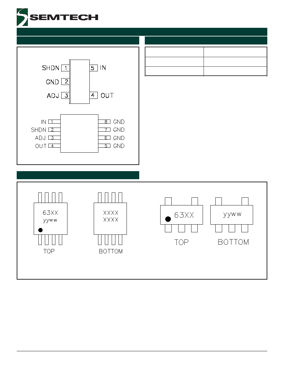
Top View
SOT-23-5
r
e
b
m
u
N
t
r
a
P
)
3
(
)
2
(
)
1
(
e
g
a
k
c
a
P
R
T
X
.
X
-
S
M
I
3
6
5
1
C
S
8
-
P
O
S
M
R
T
X
.
X
-
K
S
I
3
6
5
1
C
S
5
-
3
2
-
T
O
S
Note:
(1) Where -X.X denotes voltage options. Available
voltages are: 1.8V, 2.5V, 2.8V, 3.0V, 3.1V and 3.3V.
(2) Output voltage can be adjusted using external
resistors, see Pin Descriptions.
(3) Only available in tape and reel packaging. A reel
contains 2500 devices (MSOP-8) or 3000 devices
(SOT-23-5).
Pin Configurations
Ordering Information
MSOP-8
Marking Information
MSOP-8
SOT-23-5
63XX = SC1563, voltage option (example: 6318 for 1.8V option)
yyww = Date code (example: 0008 for week 8 of 2000)
XXXXXXXX = Lot number, not marked on SOT-23-5 (example: E01102)
5
2002 Semtech Corp.
www.semtech.com
POWER MANAGEMENT
SC1563
n
i
P
e
m
a
N
r
e
b
m
u
N
n
i
P
n
o
i
t
c
n
u
F
n
i
P
8
-
P
O
S
M
5
-
3
2
-
T
O
S
J
D
A
3
3
k
c
a
b
d
e
e
f
l
a
n
r
e
t
n
i
e
h
t
y
b
t
e
s
t
a
h
t
o
t
e
g
a
tl
o
v
t
u
p
t
u
o
e
h
t
s
t
e
s
,
d
e
d
n
u
o
r
g
n
e
h
w
,
n
i
p
s
i
h
T
n
o
it
a
c
il
p
p
A
e
e
S
(
e
b
ll
i
w
e
g
a
tl
o
v
t
u
p
t
u
o
e
h
t
,
d
e
s
u
e
r
a
s
r
o
t
s
i
s
e
r
k
c
a
b
d
e
e
f
l
a
n
r
e
t
x
e
fI
.
s
r
o
t
s
i
s
e
r
:
)
1
e
g
a
p
n
o
ti
u
c
r
i
C
D
N
G
8
-
5
2
g
n
i
k
n
i
s
t
a
e
h
r
o
f
d
e
s
u
e
b
y
a
m
s
n
i
p
e
s
e
h
T
.
s
n
i
p
8
-
P
O
S
M
ll
a
t
c
e
n
n
o
C
.
d
n
u
o
r
g
e
c
n
e
r
e
f
e
R
.
s
e
s
o
p
r
u
p
N
I
1
5
V
(
n
e
e
w
t
e
b
e
b
t
s
u
m
n
i
p
s
i
h
t
o
t
t
u
p
n
i
e
h
t
,
d
a
o
l
ll
u
f
t
a
n
o
it
a
l
u
g
e
r
r
o
F
.
e
g
a
tl
o
v
t
u
p
n
I
T
U
O
)
V
7
.
0
+
V
m
u
m
i
n
i
M
.
V
5
.
6
d
n
a
N
I
.
V
2
.
2
=
T
U
O
4
4
.
A
m
0
0
5
o
t
p
u
g
n
i
c
r
u
o
s
,
e
c
i
v
e
d
s
i
h
t
f
o
t
u
p
t
u
o
r
e
w
o
p
e
h
t
s
i
n
i
p
s
i
h
T
N
D
H
S
2
1
t
n
e
r
r
u
c
t
n
e
c
s
e
i
u
q
e
h
t
g
n
i
c
u
d
e
r
,f
f
o
r
o
t
a
l
u
g
e
r
e
h
t
s
n
r
u
t
n
e
p
o
n
i
p
s
i
h
t
g
n
i
v
a
e
L
.t
u
p
n
I
n
w
o
d
t
u
h
S
n
i
p
s
i
h
t
fi
d
e
l
b
a
n
e
e
b
ll
i
w
e
c
i
v
e
d
e
h
T
.
)
A
n
0
0
3
<
y
ll
a
c
i
p
y
t
(
e
u
l
a
v
g
n
it
a
r
e
p
o
s
ti
f
o
n
o
it
c
a
r
f
a
o
t
.
d
e
s
u
g
n
i
e
b
t
o
n
fi
D
N
G
o
t
t
c
e
n
n
o
C
.
V
4
.
0
w
o
l
e
b
d
e
ll
u
p
s
i
Volts
R2
R2)
(R1
1.200
V
OUT
+
=
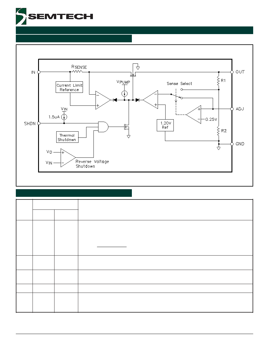
Block Diagram
Pin Descriptions