1
www.semtech.com
SC4808A/B
High Performance Dual
Ended PWM Controller
POWER MANAGEMENT
Revision July 18, 2003
Description
Features
Applications
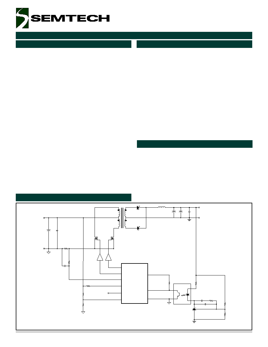
Typical Application Circuit
120µA starting current
Pulse by pulse current limit
Programmable operation up to 1MHz
Internal soft start
Programmable line undervoltage lockout
Over current shutdown
Dual output drive stages on push-pull configuration
Programmable internal slope compensation
Programmable mode of operation (peak current mode
or voltage mode)
External frequency synchronization
Bi-phase mode of operation
MSOP 10 package
-40 to 105 °C operating temperature
Telecom equipment and power supplies
Networking power supplies
Industrial power supplies
Push-pull converter
Half bridge converter
Full bridge converter
Isolated VRM's
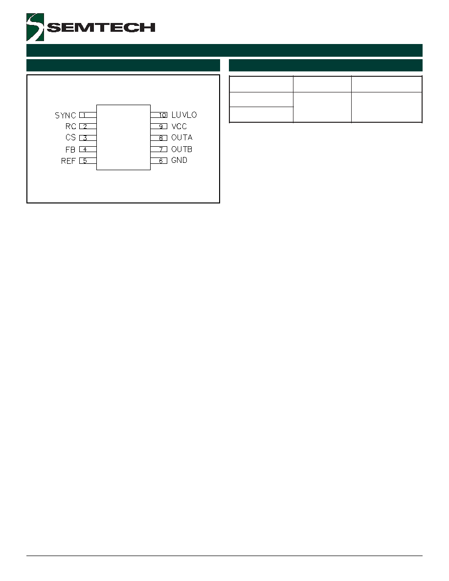
Vo
Vin
RSENSE
Gnd_Out
SYNC
Gnd_In
FB
GND
REF
LUVLO
OUTA
OUTB
CS
VCC
SYNC
RC
SC4808
The SC4808A/B is a dual-ended, high speed, highly
integrated PWM controller that is optimized for applications
requiring minimum space. The device is easily configurable
for Current or Voltage operation and contains all the control
circuitry required for isolated applications, where a
secondary side error amplifier is used.
Although simple in use, the SC4808 is fully featured and
requires only a few external components. It features,
programmable frequency up to 1MHZ, internal slope
compensation, pulse by pulse current limit, a line
monitoring input with hysteresis to reduce stress on the
power components. An internal ramp on the Current Sense
pin allows for slope compensation to be programmed
simply by an external resistor. This also allows for operation
in voltage mode.
A unique oscillator is utilized which allows two SC4808's
to be synchronized together and work out of phase. This
feature minimizes the input and output ripples, and
reduces stress and size on input/output filter components.
The outputs are configured for push-pull format, dead time
between the 2 outputs is programmable depending on the
size of the timing components.
The SC4808 features a turn on threshold of 12V (SC4808A)
& 4.4 volts (SC4808B). Both devices are available at a
MSOP-10 package.
2
2002 Semtech Corp.
www.semtech.com
SC4808A/B
POWER MANAGEMENT
Absolute Maximum Ratings
Electrical Characteristics
r
e
t
e
m
a
r
a
P
s
n
o
i
t
i
d
n
o
C
t
s
e
T
n
i
M
p
y
T
x
a
M
t
i
n
U
M
W
P
e
l
c
y
C
y
t
u
D
m
u
m
i
x
a
M
,
V
5
=
B
F
,
z
H
k
0
5
=
c
s
o
F
B
T
U
O
r
o
A
T
U
O
t
a
d
e
r
u
s
a
e
M
8
4
9
4
0
5
%
e
l
c
y
C
y
t
u
D
m
u
m
i
n
i
M
,
V
5
.
1
=
B
F
,
z
H
k
0
5
=
c
s
o
F
B
T
U
O
r
o
A
T
U
O
t
a
d
e
r
u
s
a
e
M
0
%
e
s
n
e
S
t
n
e
r
r
u
C
n
i
a
G
3
l
a
n
g
i
S
t
u
p
n
I
m
u
m
i
x
a
M
5
7
4
5
2
5
5
7
5
V
m
y
a
l
e
D
t
u
p
t
u
O
o
t
S
C
0
0
1
s
n
d
l
o
h
s
e
r
h
T
t
n
e
r
r
u
C
r
e
v
O
0
5
8
.
0
5
9
.
1
V
n
o
it
a
s
n
e
p
m
o
C
e
p
o
l
S
l
a
n
r
e
t
n
I
r
o
t
s
i
s
e
R
5
2
k
t
e
s
f
f
O
S
C
o
t
B
F
0
3
.
1
0
5
.
1
0
7
.
1
V
t
u
p
t
u
O
l
e
v
e
L
w
o
L
T
U
O
0
0
5
.
0
7
.
V
l
e
v
e
L
h
g
i
H
T
U
O
0
.
1
1
5
2
.
1
1
0
0
.
2
1
V
e
m
i
T
e
s
i
R
5
2
s
n
e
m
i
T
ll
a
F
5
2
s
n
t
u
o
k
c
o
L
e
g
a
t
l
o
V
r
e
d
n
U
C
C
V
)
A
8
0
8
4
C
S
(
d
l
o
h
s
e
r
h
T
t
r
a
t
S
5
7
.
0
1
2
1
5
2
.
3
1
V
)
A
8
0
8
4
C
S
(
s
i
s
e
r
e
t
s
y
H
5
.
3
5
.
4
5
.
5
V
)
B
8
0
8
4
C
S
(
d
l
o
h
s
e
r
h
T
t
r
a
t
S
0
.
4
0
4
.
4
5
.
4
V
)
B
8
0
8
4
C
S
(
s
i
s
e
r
e
t
s
y
H
0
4
0
7
0
1
1
V
m
r
e
t
e
m
a
r
a
P
l
o
b
m
y
S
m
u
m
i
x
a
M
s
t
i
n
U
e
g
a
tl
o
V
y
l
p
p
u
S
V
C
C
8
1
V
t
n
e
r
r
u
C
y
l
p
p
u
S
I
C
C
0
2
A
m
D
N
G
o
t
B
T
U
O
/
A
T
U
O
V
B
/
A
T
U
O
8
1
o
t
5
.
-
V
)
k
a
e
p
(
t
n
e
r
r
u
C
e
c
r
u
o
S
B
T
U
O
/
A
T
U
O
I
e
c
r
u
o
s
0
5
2
-
A
m
)
k
a
e
p
(
t
n
e
r
r
u
C
k
n
i
S
B
T
U
O
/
A
T
U
O
I
k
n
i
s
0
5
2
A
m
T
t
a
n
o
it
a
p
i
s
s
i
D
r
e
w
o
P
A
C
°
5
2
=
P
D
5
0
1
.
1
W
e
c
n
a
t
s
i
s
e
R
l
a
m
r
e
h
T
A
J
1
.
3
1
1
W
/
C
°
e
r
u
t
a
r
e
p
m
e
T
n
o
it
c
n
u
J
T
J
0
5
1
o
t
5
5
-
C
°
e
g
n
a
R
e
r
u
t
a
r
e
p
m
e
T
e
g
a
r
o
t
S
T
G
T
S
0
5
1
o
t
5
6
-
C
°
.
c
e
S
0
1
)
g
n
i
r
e
d
l
o
S
(
e
r
u
t
a
r
e
p
m
e
T
d
a
e
L
T
D
A
E
L
0
0
3
+
C
°
)
l
e
d
o
M
y
d
o
B
n
a
m
u
H
(
g
n
it
a
R
D
S
E
V
D
S
E
2
V
k
Unless specified: VCC = 12V; CL = 100pF; T
A
= -40°C to 105°C
Exceeding the specifications below may result in permanent damage to the device, or device malfunction. Operation outside of the parameters specified in
the Electrical Characteristics section is not implied.

5
2002 Semtech Corp.
www.semtech.com
SC4808A/B
POWER MANAGEMENT
FB: The inverting input to the PWM comparator. Stray in-
ductances and parasitic capacitance should be minimized
by utilizing ground planes and correct layout guide lines
(see page 22).
REF: Bandgap reference output It should be by passed with
a 2.2uF low ESR capacitance, right at the IC pin.
CS: Current sense input and internal slope compensation
are both provided via the CS pin. The current sense input
from a sense resistor is used for the peak current and
overcurrent comparators. An internal 1 to 3 feed back volt-
age divider provides a 3X amplification of the CS signal.
This is used for comparison to the external error amplifier
signal. If an external resistor is connected from CS to the
current sense resistor, the internal current source will pro-
vide a programmable slope compensation. The value of
the resistor will determine the level of compensation. At
higher compensation levels, voltage mode of operation can
be achieved.
RC: The oscillator programming pin. The oscillator should
be referenced to a stable reference voltage for an accu-
rate and stable frequency. Only two components are re-
quired to program the oscillator, a resistor (tied to Vref and
RC), and a capacitor (tied to the RC and GND). The follow-
ing formula can be used for a close approximation of the
oscillator frequency.
8
.
0
1
_
×
TOT
OSC
A
OSC
C
R
F
9
.
0
1
_
×
TOT
OSC
B
OSC
C
R
F
where:
Circuit
SC
OSC
TOT
C
C
C
C
+
+
=
4808
pF
C
SC
22
4808
Where the frequency is in Hertz, resistance in ohms, and
capacitance in farads. The recommended range of timing
resistors is between 10 kohm and 200kohm and range of
timing capacitors is between 100pF and 1000pF. Timing
resistors less than 10 kohm should be avoided.
Refer to layout guide lines on page 22 to achieve best re-
sults.
LUVLO: Line undervoltage lockout pin. An external resis-
tive divider will program the undervoltage lockout level. The
external divider should be referenced to the quiet analog
ground (see page 22). During the LUVLO, the driver out-
puts are disabled and the softstart is reset. This pin can
also function as an Enable/Disable.
SYNC: SYNC is a positive edge triggered input with a thresh-
old set to 1.6V (SC4808A), and 1.0V (SC4808B).
In a single controller operation, SYNC could be grounded
or connected to an external synchronization clock within
the SYNC frequency range (see page 3). In the Bi-Phase
operation mode SYNC pins could be connected to the Cosc
(Timing Capacitors) of the other controller. This will force
an out of phase operation (see page 15).
GND: Device power and analog ground. Careful attention
should be paid to the layout of the ground planes (see page
22).
OUTA and OUTB: Out of phase gate drive stages. The
driver's peak source and sink current drive capability of
100mA, enables the use of an external MOSFET driver or
a NPN/PNP transistor buffer.
The oscillator RC network programs the oscillator frequency,
which is twice the OUTA/OUTB frequency. To insure that
the outputs do not overlap, a dead time can be generated
between the two outputs by sizing the oscillator timing ca-
pacitor (see page 14).
VCC: The supply input for the device. Once VCC has ex-
ceeded the UVLO limit, the internal reference, oscillator,
drivers and logic are powered up. A low ESR capacitance,
should be used for decoupling right at the IC pin to mini-
mize noise problems.
Pin Descriptions