 | –≠–ª–µ–∫—Ç—Ä–æ–Ω–Ω—ã–π –∫–æ–º–ø–æ–Ω–µ–Ω—Ç: SC5826 | –°–∫–∞—á–∞—Ç—å:  PDF PDF  ZIP ZIP |

SC5826
© 2000 SEMTECH CORP.
HotSwitchTM
USB Power Distribution Switch
PRELIMINARY - February 18, 2000
652 MITCHELL ROAD NEWBURY PARK CA 91320
1
ORDERING INFORMATION
DESCRIPTION
USB power distribution switches are high-side n-
channel MOSFET switches with built-in overcurrent
protection and low on-state resistance. The SC5826
switch is designed to meet the USB requirements for
power switching and maintenance-free fault protection
for self-powered & bus-powered hub applications. The
SC5826 features low on-state resistance to meet the
USB requirement for voltage drop and regulation. The
switch is controlled by an enable input that is
compatible with 3V and 5V logic. The enable input is
available with an active high or active low input for
maximum design flexibility. The device provides short
circuit current limiting at a value of less than 1.6A, well
below the USB limit of 5A. During an overcurrent
condition the device provides a fault notification to
signal the USB controller. An integrated thermal
protection circuit automatically shuts the switch off
when the junction temperature reaches its thermal
limit. The switch remains off until the junction
temperature drops approximately 10∞C. The switch will
continue to cycle on and off until the fault is removed.
Inrush current limiting prevents the voltage drop on an
upstream port when the switch is enabled. An
undervoltage lockout circuit guarantees the switch is
initially off during start-up.
TEL:805-498-2111 FAX:805-498-3804 WEB:http://www.semtech.com
Note:
(1) Add suffix `TR' for tape and reel.
DEVICE
(1)
ENABLE
PACKAGE
SC5826-1CS
Active High
SO-8
SC5826-2CS
Active Low
SO-8
FEATURES
∑
Designed to meet USB specification 1.1 power
management requirements
∑
500mA continuous load current
∑
High-side MOSFET switch with low R
DS(ON)
∑
Short-circuit current protection
∑
Internal thermal shutdown
∑
Undervoltage lockout
∑
Logic overcurrent output
∑
Soft start circuit with slow turn-on time
APPLICATIONS
∑
Universal Serial Bus (USB) power management
∑
Self-powered or bus-powered USB hubs
∑
Root hubs in desktop PCs & servers
∑
Notebook PCs
∑
Peripherals
BLOCK DIAGRAM
PIN CONFIGURATION
Top View
(8-Pin SOIC)
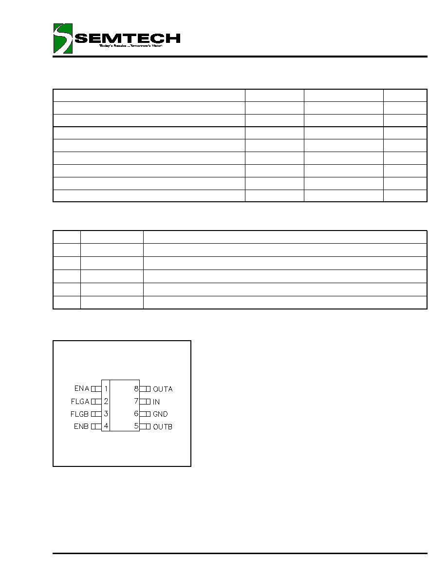
SC5826
© 2000 SEMTECH CORP.
HotSwitchTM
USB Power Distribution Switch
PRELIMINARY - February 18, 2000
652 MITCHELL ROAD NEWBURY PARK CA 91320
2
Parameter
Symbol
Maximum
Units
Input Voltage Range
V
IN
-0.3 to +7
V
Output Voltage Range`
V
OUT
-0.3 to +7
V
Enable Input
V
EN
-0.3 to +7
V
Continuous Output Current
I
O
Internally Limited
mA
Operating Ambient Temperature Range
T
A
-40 to +85
∞C
Operating Junction Temperature Range
T
J
-40 to +125
∞C
Storage Temperature Range
T
STG
-65 to +150
∞C
Lead Temperature (Soldering) 10 seconds
T
L
300
∞C
ABSOLUTE MAXIMUM RATINGS
PIN DESCRIPTION
Pin #
Pin Name
Pin Function
1, 4
ENA/ENB
Enable input: TTL compatible switch enable input.
2, 3
FLGA/FLGB
Error flag output: FLG is asserted active low during fault condition.
6
GND
Ground.
7
IN
Input voltage: Output MOSFET Drain. Connect to supply voltage.
5, 8
OUTA/OUTB
Power switch output: Output MOSFET Source. Connect to switched side of load.
PIN CONFIGURATION
Top View
(8-Pin SOIC)
SC5826
© 2000 SEMTECH CORP.
HotSwitchTM
USB Power Distribution Switch
PRELIMINARY - February 18, 2000
652 MITCHELL ROAD NEWBURY PARK CA 91320
3
ELECTRICAL CHARACTERISTICS
(1)(2)
Unless specified: T
A
= 25∞C, V
IN
= 5V, I
OA
/I
OB
= 500mA (Switches ON).
Parameter
Symbol
Conditions
Min Typ Max
Units
Power Switch
On Resistance
r
ON
4.25V
V
IN
5.50V
100 140
m
Output Leakage Current
I
L(OFF)
V
O
= 5.5V, Switches OFF
1
µA
Output Turn On Rise Time
t
R
C
O
= 1µF, R
O
= 10
1
ms
Output Turn Off Fall Time
t
F
C
O
= 1µF, R
O
= 10
0.1
1
ms
Enable Input
High Level Input Voltage
V
EN(HI)
4.25V
V
IN
5.50V
2.4
V
Low Level Input Voltage
V
EN(LO)
4.25V
V
IN
5.50V
0.8
V
Input Current
I
EN
EN = V
IN
, OUTA/B = OPEN
0
1
µA
EN = 0V, I
OA
/I
OB
= 0mA, OUTA/B = OPEN
0
1
Output Turn On Delay
t
D(ON)
0.25
ms
Output Turn Off Delay
t
D(OFF)
25
50
µs
Current Limit
Short Circuit Current Limit
I
OS
V
OA
/V
OB
= GND, Switches ON
0.65 0.90 1.60
A
Supply Current
Outputs Off
I
IN(OFF)
Switches OFF
0.02
1
µA
Outputs On
I
IN(ON)
I
OA
/I
OB
= 0mA
130 200
µA
Undervoltage Lockout
UVLO Threshold
V
UVLO
2.2
2.7
V
Hysteresis
V
HYST
90
mV
Error Flag
Output Resistance
r
FLG
I
FLG
= 10mA, V
OA
/V
OB
= GND, Switches ON
10
50
Leakage Current (Off)
I
FLG
V
FLG
= 5.0V, Switches OFF
0.01
1
µA
Over Temperature Protection
High Trip Level
T
HI
160
∞C
Hysteresis
T
HYST
10
∞C
NOTE:
(1) For SC5826-1, Switch OFF is V
EN
0.8V and Switch ON is V
EN
2.4V ("Active High").
For SC5826-2, Switch ON is V
EN
0.8V and Switch OFF is V
EN
2.4V ("Active Low").
For testing purposes EN will be 0V or V
IN
as applicable, unless otherwise specified.
(2) This device is ESD sensitive. Use of standard ESD handling precautions is required.
SC5826
© 2000 SEMTECH CORP.
HotSwitchTM
USB Power Distribution Switch
PRELIMINARY - February 18, 2000
652 MITCHELL ROAD NEWBURY PARK CA 91320
4
0.0
0.1
0.2
0.3
0.4
0.5
0.6
0.7
0.8
0.9
1.0
-50
-25
0
25
50
75
100
125
150
T
J
(∞C)
I
OS
(A)
V
IN
= 5V
2.000
2.100
2.200
2.300
2.400
2.500
2.600
2.700
2.800
2.900
3.000
-50
-25
0
25
50
75
100
125
150
T
J
(∞C)
V
UVLO
(V)
V
IN
Rising
V
IN
Falling
0
25
50
75
100
125
150
175
200
-50
-25
0
25
50
75
100
125
150
T
J
(∞C)
I
IN(ON)
(µA)
V
IN
= 5V
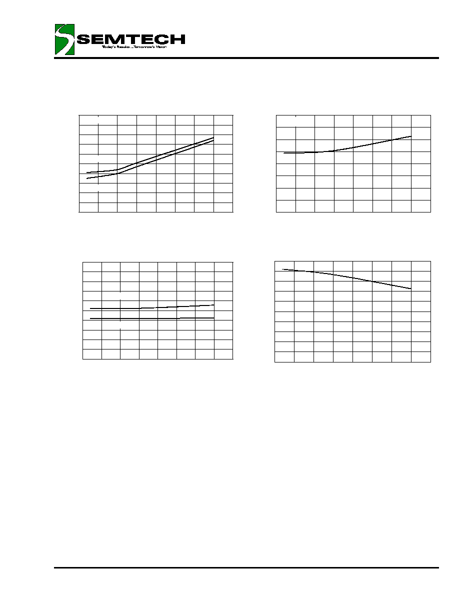
TYPICAL CHARACTERISTICS
Supply Current (Outputs On)
vs. Junction Temperature
Short Circuit Output Current
vs. Junction Temperature
UVLO Threshold vs.
Junction Temperature
50
60
70
80
90
100
110
120
130
140
150
-50
-25
0
25
50
75
100
125
150
T
J
(∞C)
r
ON
(m
)
I
O
= 0.5A
V
IN
= 4.25V
V
IN
= 5.5V
On Resistance vs. Junction Temperature
vs. Input Voltage

SC5826
© 2000 SEMTECH CORP.
HotSwitchTM
USB Power Distribution Switch
PRELIMINARY - February 18, 2000
652 MITCHELL ROAD NEWBURY PARK CA 91320
5
DETAILED DESCRIPTION
The SC5826 HotSwitchTM is a dual port, high-side
switch optimized for power control & distribution in Uni-
versal Serial Bus (USB) applications. It features an n-
channel power MOSFET with a low on-state resistance
for meeting USB voltage regulation requirements. It
available with active high (SC5826-1) or active low
(SC5826-2) inputs.
In/Out
The input is the supply voltage connection to the drain
of the power switch MOSFET. The output is con-
nected to the source of the MOSFET. Under normal
operating conditions when the power switch is enabled,
current flows from the input to the output towards the
load. The power switch is designed to sustain a mini-
mum load current of 500mA in accordance with USB
specifications.
Charge Pump
An internal charge pump powers the MOSFET gate
drive circuit and provides the necessary voltage to pull
the gate above the source.
Control Logic
The gate drive circuit controls the gate voltage of the
MOSFET power switch. The gate drive circuit also
controls the rise & fall times of the power switch output
voltage. The typical "soft start" or output voltage rise
time is 1ms.
Enable Input
A logic signal at the enable (EN) pin activates the
power MOSFET switch. A logic 1 (SC5826-1) or logic
0 (SC5826-2) will bias the charge pump, gate drive,
and control circuitry turning on the power switch. A
logic signal of opposite polarity turns off the switch. If
both outputs are off, the device powers down. The en-
able input is compatible with 3V & 5V logic levels.
Error Flag
The error flag (FLG) output is an n-channel, open drain
MOSFET. The FLG pin is an active low during short
circuit, undervoltage, or thermal shutdown conditions.
The output remains low until the fault condition is re-
moved.
Thermal Sense
An internal thermal shutdown circuit turns off the power
switch output MOSFET when the die junction tempera-
ture exceeds 160∞C. The output FLG pin is asserted
to a logic low signaling a fault condition. A built in hys-
teresis prevents the switch from turning on until the die
temperature has cooled approximately 10∞C. The
switch will continue to cycle on and off until the fault
condition is removed. The thermal sense circuit func-
tions only when the switch is enabled.
Undervoltage Lockout
An undervoltage lockout circuit monitors the input volt-
age and prevents the power switch MOSFET from
turning on until the input voltage (IN) exceeds 2.5V
(typical). If the input voltage falls 90mV (typical) below
that point after the switch has been turned on, the un-
dervoltage lockout turns off the power switch output
MOSFET and asserts the FLG output to logic low. The
undervoltage lockout functions only when the switch is
enabled.