
1
United States Patent No. 6,504,422
www.semtech.com
POWER MANAGEMENT
5+$!
CHARGE PUMP REGULATOR WITH
SELECTABLE 5.0V/4.5V OUTPUT
Revision 2, .ebruary 2003
Description
.eatures
Applications
Typical Application Circuit
The SC603 is a versatile charge pump designed for use in
battery operated power supply applications. The wide input
range is matched for Li-Ion battery applications. Only two tiny
ceramic bucket capacitors are required, and the inductorless
implementation provides a reduced-EMI solution. Patented low
noise mode switching circuitry and constant output current allow
the use of extremely small input and output capacitors.
The SC603
charge pump regulator can be used for applications
that require up to 200mA of output current with a 4.5V output.
The 5.0V output version provides up to 160mA of output
current.
Compared to a switch mode regulator, the SC603 offers a
solution with less cost, area, noise and complexity.
KSmall size - MLP Micro 10 lead 3x3mm package
KSelectable 5.0V or 4.5V output voltage
K200mA available with 4.5V output
K160mA available with 5.0V output
KShort circuit protection
KSoft Start function
KShutdown current <2�A
KSelectable fixed frequencies of 262kHz and 650kHz
KLow ripple
KRegulated to +/-5%
KEase of use
KCellular phones
KLED photo flash for cellular phones
KLED backlighting
KPDA power supplies
KPortable electronics
KElectronic books
KWireless web appliances
Cin
1.0u.
2.7V to 6.5V
Cbucket1
1.0u.
Cbucket2
1.0u.
VIN
EN
VSEL
.SEL
GND
C.2-
C.2+
C.1-
C.1+
VOUT
3
6
4
5
8
7
10
9
2
1
U1
5
+
$
!
Cout
1.0u.
UP TO 10 LEDS
4.5V or 5.0V

2
2003 Semtech Corp.
United States Patent No. 6,504,422
www.semtech.com
5+$!
POWER MANAGEMENT
Absolute Maximum Ratings
Electrical Characteristics
r
e
t
e
m
a
r
a
P
l
o
b
m
y
S
m
u
m
i
x
a
M
s
ti
n
U
e
g
a
tl
o
V
y
l
p
p
u
S
V
N
I
0
.
7
+
o
t
3
.
0
-
V
e
g
a
tl
o
V
t
u
p
t
u
O
V
T
U
O
0
.
7
+
o
t
3
.
0
-
V
V
T
U
O
n
o
it
a
r
u
D
ti
u
c
ri
C
t
r
o
h
S
C
S
e
ti
n
if
e
d
n
I
t
n
e
i
b
m
A
o
T
n
o
it
c
n
u
J
,
e
c
n
a
t
s
i
s
e
R
l
a
m
r
e
h
T
)
d
o
h
t
e
M
d
r
a
d
n
a
t
S
1
5
D
S
E
J
(
A
J
1
3
W
/
C
�
t
n
e
i
b
m
A
g
n
it
a
r
e
p
O
T
A
5
8
+
o
t
0
4
-
C
�
e
g
n
a
R
e
r
u
t
a
r
e
p
m
e
T
n
o
it
c
n
u
J
T
C
J
0
5
1
+
o
t
0
4
-
C
�
e
g
n
a
R
e
r
u
t
a
r
e
p
m
e
T
e
g
a
r
o
t
S
T
G
T
S
0
5
1
+
o
t
5
6
-
C
�
e
r
u
t
a
r
e
p
m
e
T
d
a
e
L
T
D
A
E
L
0
0
3
C
�
r
e
t
e
m
a
r
a
P
l
o
b
m
y
S
s
n
o
i
t
i
d
n
o
C
N
I
M
P
Y
T
X
A
M
s
t
i
n
U
e
g
a
tl
o
V
y
l
p
p
u
S
t
u
p
n
I
V
N
I
5
.
2
5
.
6
V
t
n
e
r
r
u
C
t
n
e
c
s
e
i
u
Q
I
Q
I
,
z
H
k
2
6
2
=
.
q
e
r
.
T
U
O
V
,
A
m
0
=
N
I
V
7
.
3
=
0
.
1
4
.
1
A
m
I
,
z
H
k
0
5
6
=
.
q
e
r
.
T
U
O
V
,
A
m
0
=
N
I
V
7
.
3
=
1
.
2
8
.
2
A
m
0
=
e
l
b
a
n
E
2
A
�
e
g
a
tl
o
V
t
u
p
t
u
O
V
T
U
O
h
ti
w
n
o
it
a
l
u
g
e
R
d
a
o
L
c
it
a
t
S
1
=
L
E
S
V
5
7
.
4
0
.
5
5
2
.
5
V
h
ti
w
n
o
it
a
l
u
g
e
R
d
a
o
L
c
it
a
t
S
0
=
L
E
S
V
5
7
2
.
4
5
.
4
5
2
7
.
4
V
t
n
e
r
r
u
C
t
u
p
t
u
O
I
T
U
O
V
<
V
2
.
3
,
1
=
L
E
S
V
N
I
V
5
.
5
<
0
5
1
A
m
V
<
V
2
.
3
,
1
=
L
E
S
V
N
I
V
5
.
5
<
T
A
0
4
-
=
o
0
7
o
t
C
o
C
0
6
1
A
m
V
<
V
2
.
3
,
0
=
L
E
S
V
N
I
V
5
.
5
<
0
9
1
A
m
V
<
V
2
.
3
,
0
=
L
E
S
V
N
I
V
5
.
5
<
T
A
0
4
-
=
o
0
7
o
t
C
o
C
0
0
2
A
m
V
<
V
5
8
.
2
,
1
=
L
E
S
V
N
I
V
5
.
5
<
0
6
A
m
V
<
V
5
8
.
2
,
0
=
L
E
S
V
N
I
V
5
.
5
<
0
2
1
A
m
y
c
n
e
u
q
e
r
.
p
m
u
P
f
P
M
U
P
0
=
L
E
S
.
,
1
=
e
l
b
a
n
E
%
5
1
-
2
6
2
%
5
1
+
z
H
k
1
=
L
E
S
.
,
1
=
e
l
b
a
n
E
%
0
2
-
0
5
6
%
0
2
+
z
H
k
e
m
i
T
n
o
it
i
s
n
a
r
T
e
d
o
M
y
c
n
e
u
q
e
r
.
T
K
C
O
L
y
c
n
e
u
q
e
r
f
e
n
o
m
o
r
f
e
m
it
n
o
it
i
s
n
a
r
T
e
d
o
m
y
c
n
e
u
q
e
r
f
r
e
h
t
o
y
n
a
o
t
e
d
o
m
n
g
i
s
e
d
y
b
d
e
e
t
n
a
r
a
u
g
1
d
o
ir
e
P
t
n
e
r
r
u
C
ti
u
c
r
i
C
t
r
o
h
S
I
C
S
V
T
U
O
I
,
V
0
=
T
U
O
I
=
N
I
0
0
6
A
m
d
l
o
h
s
e
r
h
T
h
g
i
H
t
u
p
n
I
V
H
I
)
L
E
S
.
,
L
E
S
V
,
e
l
b
a
n
E
(
s
n
i
p
t
u
p
n
i
ll
A
3
.
1
V
Unless specified: T
A
= -40�C to 85�C, Cin=Cbucket = 1.0�. (ESR = 0.1
), Cout=1.0u. (ESR = 0.1
), Vin= 2.85V to 5.5V
3
2002 Semtech Corp.
United States Patent No. 6,504,422
www.semtech.com
5+$!
POWER MANAGEMENT
Note:
(1) Peak to peak output ripple voltage with C
OUT
=C
BUCKET
=1u. and X5R dielectric
(2) Guaranteed by design
(3) This device is ESD sensitive. Use of standard ESD handling precautions is required.
E
C
I
V
E
D
E
C
I
V
E
D
E
C
I
V
E
D
E
C
I
V
E
D
E
C
I
V
E
D
)
2
(
)
1
(
)
2
(
)
1
(
)
2
(
)
1
(
)
2
(
)
1
(
)
2
(
)
1
(
E
G
A
K
C
A
P
E
G
A
K
C
A
P
E
G
A
K
C
A
P
E
G
A
K
C
A
P
E
G
A
K
C
A
P
R
T
L
M
I
3
0
6
C
S
m
m
3
x
3
0
1
-
P
L
M
B
V
E
3
0
6
C
S
d
r
a
o
B
n
o
it
a
u
l
a
v
E
Pin Configuration
Ordering Information
Note:
(1) Only available in tape and reel.
(2) A reel of MLP-10 contains 3000 devices.
Pin Descriptions
n
i
P
e
m
a
N
n
i
P
n
o
i
t
c
n
u
.
n
i
P
1
T
U
O
V
V
5
.
4
r
o
V
0
.
5
o
t
d
e
t
a
l
u
g
e
r
e
g
a
tl
o
v
t
u
p
t
u
O
2
+
1
.
C
1
r
o
ti
c
a
p
a
c
t
e
k
c
u
b
f
o
l
a
n
i
m
r
e
t
e
v
it
i
s
o
P
3
N
I
V
V
5
.
6
o
t
V
5
.
2
m
o
r
f
g
n
i
g
n
a
r
e
g
a
tl
o
v
t
u
p
n
I
4
L
E
S
.
;
z
H
k
2
6
2
=
q
e
r
f
,
0
=
L
E
S
.
.y
c
n
e
u
q
e
r
f
l
a
n
o
it
a
r
e
p
o
e
h
t
g
n
it
c
e
l
e
s
r
o
f
t
u
p
n
i
c
i
g
o
L
z
H
k
0
5
6
=
q
e
r
f
,
1
=
L
E
S
.
5
L
E
S
V
V
5
.
4
=
T
U
O
V
,
0
=
L
E
S
V
;
V
5
=
T
U
O
V
,
1
=
L
E
S
V
.
e
g
a
tl
o
v
t
u
p
t
u
o
e
h
t
g
n
it
c
e
l
e
s
r
o
f
t
u
p
n
i
c
i
g
o
L
6
N
E
.
w
o
l
t
e
s
n
e
h
w
A
u
2
n
a
h
t
s
s
e
l
s
i
t
n
e
r
r
u
c
s
a
i
B
.
e
l
b
a
n
e
h
g
i
h
e
v
it
c
A
7
-
2
.
C
2
r
o
ti
c
a
p
a
c
t
e
k
c
u
b
f
o
l
a
n
i
m
r
e
t
e
v
it
a
g
e
N
8
D
N
G
d
n
u
o
r
G
9
-
1
.
C
1
r
o
ti
c
a
p
a
c
t
e
k
c
u
b
f
o
l
a
n
i
m
r
e
t
e
v
it
a
g
e
N
0
1
+
2
.
C
2
r
o
ti
c
a
p
a
c
t
e
k
c
u
b
f
o
l
a
n
i
m
r
e
t
e
v
it
i
s
o
P
r
e
t
e
m
a
r
a
P
l
o
b
m
y
S
s
n
o
it
i
d
n
o
C
N
I
M
P
Y
T
X
A
M
s
ti
n
U
d
l
o
h
s
e
r
h
T
w
o
L
t
u
p
n
I
V
L
I
)
L
E
S
.
,
L
E
S
V
,
e
l
b
a
n
E
(
s
n
i
p
t
u
p
n
i
ll
A
4
.
0
V
t
n
e
rr
u
C
h
g
i
H
t
u
p
n
I
I
H
I
)
L
E
S
.
,
L
E
S
V
,
e
l
b
a
n
E
(
s
n
i
p
t
u
p
n
i
ll
A
0
1
A
�
t
n
e
rr
u
C
w
o
L
t
u
p
n
I
I
L
I
)
L
E
S
.
,
L
E
S
V
,
e
l
b
a
n
E
(
s
n
i
p
t
u
p
n
i
ll
A
0
1
A
�
o
t
y
r
e
tt
a
B
m
o
rf
y
c
n
e
i
c
if
f
E
r
e
w
o
P
t
u
p
t
u
O
p
m
u
P
e
g
r
a
h
C
d
e
t
a
l
u
g
e
R
V
N
I
V
,
V
3
.
3
=
T
U
O
I
,
V
0
.
5
=
T
U
O
A
m
0
6
=
z
H
k
2
6
2
=
.
q
e
r
.
0
.
5
7
%
V
N
I
V
,
V
3
.
3
=
T
U
O
I
,
V
0
.
5
=
T
U
O
A
m
0
6
=
z
H
k
0
5
6
=
.
q
e
r
.
5
.
4
7
%
e
g
a
tl
o
V
e
l
p
p
i
R
t
u
p
t
u
O
V
P
P
I
,
z
H
k
2
6
2
=
q
e
rf
T
U
O
A
m
0
6
=
)
2
(
,)
1
(
5
2
5
4
V
m
Unless specified: T
A
= -40�C to 85�C, Cin=Cbucket = 1.0�. (ESR = 0.1
), Cout=1.0u. (ESR = 0.1
), Vin= 2.85V to 5.5V
MLP10: 3X3 10 LEAD
TOP VIEW
10
9
8
7
6
5
1
2
3
4
VOUT
VIN
.SEL
VSEL
C.1-
GND
C.2+
C.2-
EN
C.1+
4
2003 Semtech Corp.
United States Patent No. 6,504,422
www.semtech.com
5+$!
POWER MANAGEMENT
Comparison with Other Regulation Methods
In many instances, a charge pump regulator is the best choice for portable power applications. These regulators offer many
advantages over switch mode regulators. A smaller bill of materials, less layout area, lower component height, less noise, no EM.,
and less overall circuit cost are typical reasons to use this type of regulation. The efficiency of a charge pump regulator often
approaches and in some cases exceeds the efficiency of a switch mode regulator.
Inductors are often the largest and most expensive discrete component in a design. There are no inductors used in the SC603, so
the inductors cost and layout area are eliminated. The noise and EM. associated with the inductor are also eliminated.
The SC603s fixed frequency harmonics are an advantage in portable communications equipment, such as cellular telephones.
The SC603 has distinct frequencies of operation, so the harmonics are predictable. The harmonics are not fixed in a switch mode
regulator. Switch mode regulators have harmonics which vary due to the pulse width modulation used to regulate the output.
Varying harmonics can be a problem because it may be more difficult to ensure acceptable noise performance over the entire
operating range.
Many switch mode regulators have increased voltage ripple on the output during pulse skipping mode due to the fact that there are
large periods of time when no current is supplied to the output. The SC603 supplies current to the output continuously, so the
voltage ripple is less than a switch mode regulator, even with greatly reduced output capacitance.
.requency Selection
The .SEL input is for frequency selection. A logic High level at this input will set the clock frequency to 650kHz, while a logic Low
sets the clock to 262kHz. Input from a uP or other device may be used to change the charge pump frequency at any time. The
optimal frequency will depend upon the capacitor values, the load current, and the exceptable amount of output ripple.
Ripple Performance
Examples of the output ripple, charge pump frequency and capacitor size are listed in Table 2 Ripple Performance.
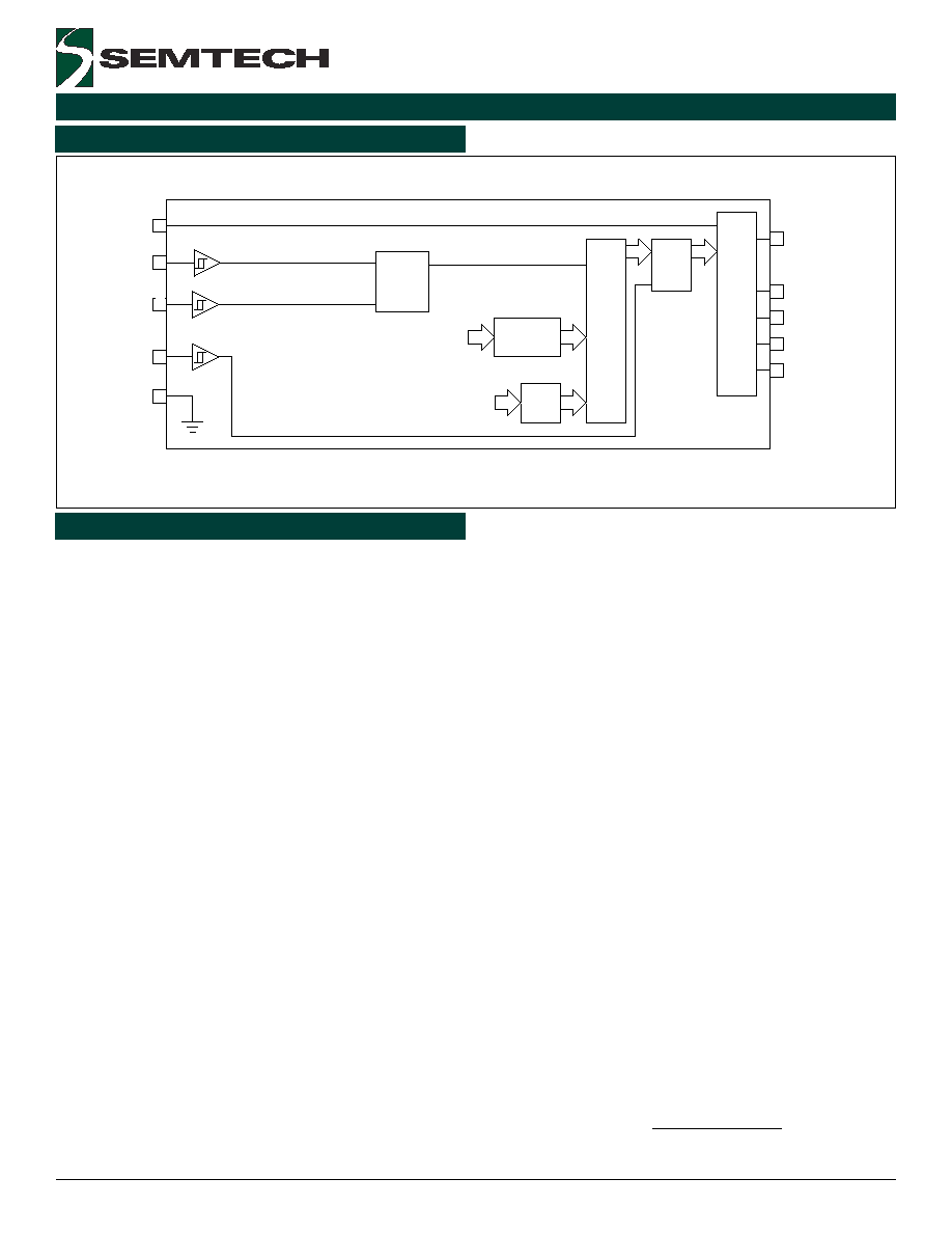
Block Diagram
Applications Information
The SC603 uses a voltage doubler circuit which is implemented with two switched or bucket capactors. Most charge pump
doublers use only one bucket capacitor. Two bucket capacitors switching on alternate phases greatly reduce the output ripple
voltage.
The output is prevented from exceeding 6.0V. This feature allows the use of 6.3V ceramic capacitors.
EN
.SEL
VSEL
GND
VIN
6
5
4
8
3
MODE
SELECT
DRIVERS
SWITCH
BLOCK
TIMER
COMPARATORS
VIN
VOUT
VRE.
VIN
C.1+
C.1-
C.2+
C.2-
VOUT
2
9
10
7
1
EN
OSC
650kHz or 262kHz
5.0V or 4.5V
"
#
5
2002 Semtech Corp.
United States Patent No. 6,504,422
www.semtech.com
5+$!
POWER MANAGEMENT
=
Efficiency
Efficiency for the SC603 is defined as,
Table 2 -Ripple Performance
V
T
U
O
]
z
H
k
[
.
q
e
r
.
]
A
m
[
t
u
o
I
]
p
-
p
V
m
[
e
l
p
p
i
R
t
u
p
u
O
C
T
U
O
]
.
u
[
C
T
E
K
C
U
B
]
.
u
[
V
0
.
5
2
6
2
0
0
1
5
2
1
1
0
5
6
0
0
1
5
1
1
1
2
6
2
0
5
1
0
5
1
1
0
5
6
0
5
1
5
2
1
1
V
5
.
4
2
6
2
0
0
1
5
2
1
1
0
5
6
0
0
1
5
1
1
1
2
6
2
0
0
2
0
6
1
1
0
5
6
0
0
2
0
3
1
1
V
O
I
O
V
IN
2 I
O
I
Q
+
(
)
Design and Layout Considerations
The layout should be patterned after the evaluation board gerber plots shown on page 7. The center pad thermal slug is not
internally connected to ground, but is connected to ground in the layout through a via centered on the pad and connecting to the
ground plane. Pin 8 is then routed directly to the center pad. A good ground plane connection is important to make effective use of
the low thermal resistance of the MLP package.
Short Circuit and Over Temperature Protection
The output is current limited to 600mA to protect against short circuit conditions. Over temperature protection is also provided.
where V
O
= output voltage
I
O
= output current
V
IN
= input voltage
I
Q
= quiescent current [from Electrical Characteristics on page 2]
Calculating Power Dissipation
The power dissipated by the SC603 is calculated as,
2
IN
2
OUT
-
2
D
2
D
8
IN
2
1
O
1
Q
+
(
)
8
O
1
O
-
=
=