
150mA ULTRA LOW DROPOUT,
LOW NOISE REGULATOR
© 2000 SEMTECH CORP.
652 MITCHELL ROAD NEWBURY PARK CA 91320
SC8863
March 1, 2000
1
Notes:
(1) Where -XXX denotes voltage options. Available
voltages are: 2.50V (-250), 2.80V (-280), 3.00V (-300),
and 3.30 (-330)V.
(2) Add suffix `TR' for tape and reel.
DESCRIPTION
The SC8863 is a low dropout linear regulator that
operates from a +2.5V to +5.5V input range and
delivers up to 150mA. A PMOS pass transistor allows
the low 110µA supply current to remain independent of
load, making these devices ideal for battery operated
portable equipment such as cellular phones, cordless
phones and personal digital assistants.
The SC8863 output voltage can be preset or adjusted
with an external resistor divider. Other features include
low powered shutdown, short circuit protection, thermal
shutdown protection and reverse battery protection.
The SC8863 comes in the tiny 5 lead SOT-23
package.
FEATURES
∑
Guaranteed 150 mA output current
∑
Fixed or adjustable output
∑
Very small external components
∑
Low 75µV
RMS
output noise
∑
Very low supply current
∑
Thermal overload protection
∑
Reverse battery protection
∑
Low power shutdown
∑
Surface mount packaging (5 pin SOT-23)
∑
Full industrial temperature range
∑
Battery Powered Systems
∑
Cellular Telephones
∑
Cordless Telephones
∑
Personal Digital Assistants
∑
Portable Instrumentation
∑
Modems
∑
PCMCIA cards
PIN CONFIGURATION
TEL:805-498-2111 FAX:805-498-3804 WEB:http://www.semtech.com
Part Number
Package
SC8863-XXXCSK
(1)(2)
SOT-23-5
ORDERING INFORMATION
BLOCK DIAGRAM
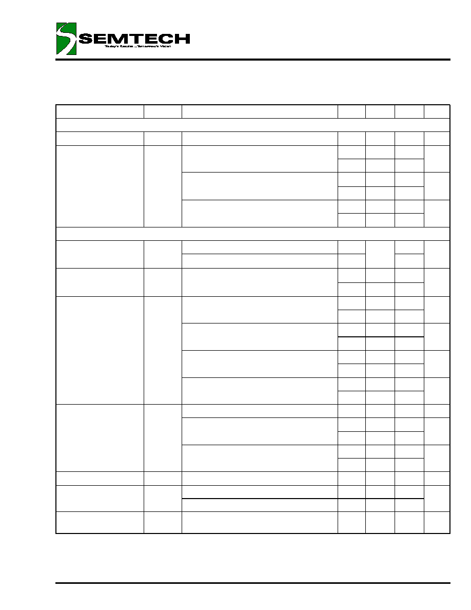
ABSOLUTE MAXIMUM RATINGS
APPLICATIONS
Parameter
Symbol
Maximum
Units
Input Supply Voltage
V
IN
-0.6 to +7
V
Power Dissipation
T
A
= 70∞C
P
D
571
mW
Thermal Resistance
JA
256
∞C/W
JC
81
∞C/W
Operating Ambient
Temperature Range
T
A
-40 to +85
∞C
Operating Junction
Temperature Range
T
J
-40 to +150
∞C
Storage Temperature
Range
T
STG
-65 to +150
∞C
Lead Temperature
(Soldering) 10 Sec
T
LEAD
+300
∞C
ESD Rating
ESD
1.25
kV

150mA ULTRA LOW DROPOUT,
LOW NOISE REGULATOR
© 2000 SEMTECH CORP.
652 MITCHELL ROAD NEWBURY PARK CA 91320
SC8863
March 1, 2000
2
PIN DESCRIPTIONS
Pin #
Pin Name
Description
1
EN
Active high enable pin. Connect to VIN if not being used.
2
GND
Ground pin. Can be used for heatsinking if needed.
3
IN
Input pin.
4
OUT
Regulator output, sourcing up to 150mA
5
SET
Connecting this pin to ground results in the internally preset value for
V
OUT
. Connecting to an external resistor divider changes V
OUT
to:
TYPICAL APPLICATION - EXTERNALLY SET OUTPUT VOLTAGE
(1)
TYPICAL APPLICATION - INTERNALLY PRESET OUTPUT VOLTAGE
VIN > VOUT + VD(MAX)
VOUT @ IOUT up to 150mA
U1
SC8863
1
2
3
4
5
EN
GND
VIN
VO
SET
C1
1uF Ceramic
C2
1uF Ceramic
+
∑
=
2
R
1
R
1
250
.
1
V
OUT
NOTES:
(1) Select R1 and R2 such that the current flowing through them is
10µA (i.e. R2
120k
). A value of 10k
is
recommended for R2. Please see Component Selection - Externally Set Output.
VOUT @ IOUT up to 150mA
VIN > VOUT + VD(MAX)
C2
2.2uF Ceramic
U1
SC8863
1
2
3
4
5
EN
GND
VIN
VO
SET
R1
R2
10k
C1
1uF Ceramic
150mA ULTRA LOW DROPOUT,
LOW NOISE REGULATOR
© 2000 SEMTECH CORP.
652 MITCHELL ROAD NEWBURY PARK CA 91320
SC8863
March 1, 2000
3
ELECTRICAL CHARACTERISTICS
Unless specified: V
IN
= 3.6V, V
SET
= GND, V
EN
= V
IN
, T
A
= 25∞C. Values in bold apply over full operating ambient temperature range.
Parameter
Symbol
Conditions
Min
Typ
Max
Units
IN
Supply Voltage Range
V
IN
2.5
5.5
V
Supply Current
I
Q
I
OUT
= 0mA
100
130
µA
160
50mA
I
OUT
150mA
110
160
µA
200
V
EN
= 0V
0.0001
1
µA
2
OUT
Output Voltage
(1)
V
OUT
I
OUT
= 1mA
-2.0%
V
OUT
+2.0%
V
1mA
I
OUT
150mA, V
OUT
+1V
V
IN
5.5V
-3.5%
+3.5%
Line Regulation
(1)
REG
(LINE)
2.5V
V
IN
5.5V, SET = OUT, I
OUT
= 1mA
5
10
mV
12
Load Regulation
(1)
REG
(LOAD)
I
OUT
= 0mA to 50mA
-10
-15
mV
-20
I
OUT
= 0mA to 100mA
-15
-20
mV
-25
I
OUT
= 0mA to 50mA, SET = OUT
-2.5
-7.5
mV
-15.0
I
OUT
= 0mA to 100mA, SET = OUT
-5
-15
mV
-30
Dropout Voltage
(1)(2)
V
D
I
OUT
= 1mA
1.1
mV
I
OUT
= 50mA
55
90
mV
120
I
OUT
= 100mA
110
180
mV
240
Current Limit
I
LIM
150
240
350
mA
Output Voltage Noise
e
n
10Hz to 99kHz, I
OUT
= 50mA, C
OUT
= 1µF
90
µV
RMS
C
OUT
= 100µF
75
Power Supply Rejection
Ratio
PSRR
f
1kHz
55
dB
150mA ULTRA LOW DROPOUT,
LOW NOISE REGULATOR
© 2000 SEMTECH CORP.
652 MITCHELL ROAD NEWBURY PARK CA 91320
SC8863
March 1, 2000
4
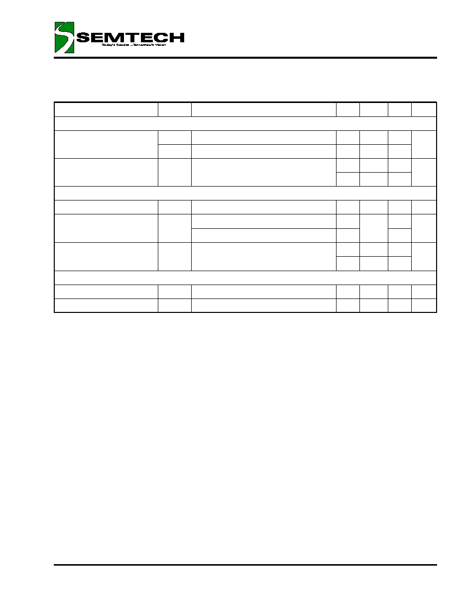
ELECTRICAL CHARACTERISTICS (Cont.)
Unless specified: V
IN
= 3.6V, V
SET
= GND, V
EN
= V
IN
, T
A
= 25∞C. Values in bold apply over full operating ambient temperature range.
Parameter
Symbol
Conditions
Min
Typ
Max Units
EN
EN Input Threshold
V
IH
1.8
V
V
IL
0.4
EN Input Bias Current
(3)
I
EN
EN = V
IN
0
100
nA
200
SET
Sense/Select Threshold
V
TH
20
55
80
mV
SET Reference Voltage
(1)
V
SET
I
OUT
= 1mA
1.225 1.250 1.275
V
1mA
I
OUT
150mA, 2.5V
V
IN
5.5V
1.206
1.294
SET Input Leakage Current
(3)
I
SET
SET
= 1.3V
0.015 2.500
nA
5.000
OVER TEMPERATURE PROTECTION
High Trip Level
T
HI
170
∞C
Hysteresis
T
HYST
10
∞C
NOTE:
(1) Low duty cycle pulse resting with Kelvin corrections required.
(2) Defined as the input to output differential at which the output voltage drops 100mV below the value measured at
a differential of 2V.
(3) Guaranteed by design.

150mA ULTRA LOW DROPOUT,
LOW NOISE REGULATOR
© 2000 SEMTECH CORP.
652 MITCHELL ROAD NEWBURY PARK CA 91320
SC8863
March 1, 2000
5
TYPICAL CHARACTERISTICS
2.74
2.75
2.76
2.77
2.78
2.79
2.80
2.81
2.82
2.83
2.84
2.85
2.86
0
25
50
75
100
125
150
I
OUT
(mA)
V
OUT
(V)
V
IN
= 3.6V
T
J
= 25∞C
Output Voltage vs. Output Current
2.74
2.75
2.76
2.77
2.78
2.79
2.80
2.81
2.82
2.83
2.84
2.85
2.86
-50
-25
0
25
50
75
100
125
T
J
(∞C)
V
OUT
(V)
IO = 1mA
IO = 50mA
IO = 100mA
IO = 150mA
V
IN
= 3.6V
Output Voltage vs. Junction
Temperature vs. Output Current
1.210
1.220
1.230
1.240
1.250
1.260
1.270
1.280
1.290
-50
-25
0
25
50
75
100
125
T
J
(∞C)
V
SET
(V)
IO = 1mA
IO = 50mA
IO = 100mA
IO = 150mA
V
IN
= 3.6V
SET Reference Voltage vs. Junction
Temperature vs. Output Current
1.225
1.230
1.235
1.240
1.245
1.250
1.255
1.260
1.265
1.270
1.275
0
25
50
75
100
125
150
I
OUT
(mA)
V
SET
(V)
V
IN
= 3.6V
T
J
= 25∞C
SET Reference Voltage vs.
Output Current
0
2
4
6
8
10
12
-50
-25
0
25
50
75
100
125
T
J
(∞C)
REG
(LINE)
(mV)
V
IN
= 2.5V to 5.5V
SET = OUT
I
OUT
= 1mA
Line Regulation vs.
Junction Temperature
0
25
50
75
100
125
150
175
200
225
250
0
25
50
75
100
125
150
I
OUT
(mA)
V
D
(mV)
-40∞C
25∞C
125∞C
SET = GND
Dropout Voltage vs. Output Current
vs. Junction Temperature