PROTECTION PRODUCTS
1
www.semtech.com
PROTECTION PRODUCTS
SLVU2.8
Low Voltage EPD TVS Diode
For ESD and Latch-Up Protection
Description
Features
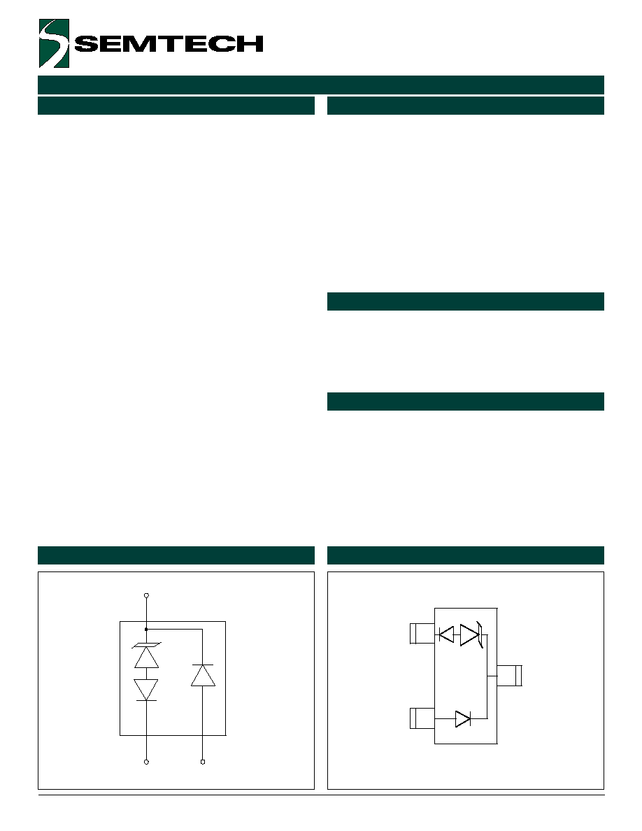
Circuit Diagram
Schematic & PIN Configuration
Revision 9/2000
The SLV series of transient voltage suppressors are
designed to protect low voltage, state-of-the-art CMOS
semiconductors from transients caused by electro-
static discharge (ESD), cable discharge events (CDE),
lightning and other induced voltage surges.
The devices are constructed using Semtechs propri-
etary EPD process technology. The EPD process pro-
vides low standoff voltages with significant reductions
in leakage currents and capacitance over silicon-
avalanche diode processes. The SLVU2.8 features an
integrated low capacitance compensation diode that
allows the device to be configured to protect one
unidirectional line or, when paired with a second
SLVU2.8, two high-speed line pairs. The low capaci-
tance design of the SLVU2.8 means signal integrity is
preserved in high-speed applications such as 10/100
Ethernet.
The SLVU2.8 is in an SOT23 package and has a low
2.8 volt working voltage. It is specifically designed to
protect low voltage components such as Ethernet
transceivers, laser diodes, ASICs, and high-speed RAM.
The low clamping voltage of the SLVU2.8 minimizes the
stress on the protected IC.
The SLV series TVS diodes will exceed the surge re-
quirements of IEC 61000-4-2, Level 4.
Applications
Mechanical Characteristics
u
10/100 Ethernet
u
WAN/LAN Equipment
u
Switching Systems
u
Desktops, Servers, Notebooks & Handhelds
u
Laser Diode Protection
u
Base Stations
u
400 Watts peak pulse power (tp = 8/20�s)
u
Transient protection for high speed data lines to
IEC 61000-4-2 (ESD) 15kV (air), 8kV (contact)
IEC 61000-4-4 (EFT) 40A (tp = 5/50ns)
IEC 61000-4-5 (Lightning) 24A (tp = 8/20�s)
u
One device protects one unidirectional line
u
Two devices protect two high-speed line pairs
u
Low capacitance
u
Low leakage current
u
Low operating and clamping voltages
u
Solid-state EPD TVS process technology
u
JEDEC SOT23 package
u
Molding compound flammability rating: UL 94V-0
u
Marking : U2.8
u
Packaging : Tape and Reel per EIA 481
SOT23 (Top View)
3
1
2
3
1
2

2
� 2000 Semtech Corp.
www.semtech.com
PROTECTION PRODUCTS
PROTECTION PRODUCTS
SLVU2.8
Absolute Maximum Rating
Electrical Characteristics
g
n
it
a
R
l
o
b
m
y
S
e
u
l
a
V
s
ti
n
U
0
2
/
8
=
p
t(
r
e
w
o
P
e
s
l
u
P
k
a
e
P
m )
s
P
k
p
0
0
4
s
tt
a
W
0
2
/
8
=
p
t(
t
n
e
rr
u
C
e
s
l
u
P
k
a
e
P
m )
s
I
P
P
4
2
A
e
r
u
t
a
r
e
p
m
e
T
g
n
ir
e
d
l
o
S
d
a
e
L
T
L
)
s
d
n
o
c
e
s
0
1
(
0
6
2
o
C
e
r
u
t
a
r
e
p
m
e
T
g
n
it
a
r
e
p
O
T
J
5
2
1
+
o
t
5
5
-
o
C
e
r
u
t
a
r
e
p
m
e
T
e
g
a
r
o
t
S
T
G
T
S
0
5
1
+
o
t
5
5
-
o
C
8
.
2
U
V
L
S
r
e
t
e
m
a
r
a
P
l
o
b
m
y
S
s
n
o
it
i
d
n
o
C
m
u
m
i
n
i
M
l
a
c
i
p
y
T
m
u
m
i
x
a
M
s
ti
n
U
e
g
a
tl
o
V
ff
O
-
d
n
a
t
S
e
s
r
e
v
e
R
V
M
W
R
1
o
t
2
n
i
P
r
o
1
o
t
3
n
i
P
8
.
2
V
e
g
a
tl
o
V
h
g
u
o
r
h
T
-
h
c
n
u
P
V
T
P
I
T
P
1
o
t
3
n
i
P
,
A
�
2
=
0
.
3
V
e
g
a
tl
o
V
k
c
a
B
-
p
a
n
S
V
B
S
I
B
S
1
o
t
3
n
i
P
,
A
m
0
5
=
8
.
2
V
t
n
e
rr
u
C
e
g
a
k
a
e
L
e
s
r
e
v
e
R
I
R
V
M
W
R
C
�
5
2
=
T
,
V
8
.
2
=
1
o
t
2
n
i
P
r
o
1
o
t
3
n
i
P
1
A
�
e
g
a
tl
o
V
g
n
i
p
m
a
l
C
V
C
I
P
P
s
�
0
2
/
8
=
p
t
,
A
2
=
1
o
t
3
n
i
P
9
.
3
V
e
g
a
tl
o
V
g
n
i
p
m
a
l
C
V
C
I
P
P
s
�
0
2
/
8
=
p
t
,
A
5
=
1
o
t
3
n
i
P
7
V
e
g
a
tl
o
V
g
n
i
p
m
a
l
C
V
C
I
P
P
s
�
0
2
/
8
=
p
t
,
A
4
2
=
1
o
t
3
n
i
P
5
.
2
1
V
e
g
a
tl
o
V
g
n
i
p
m
a
l
C
V
C
I
P
P
s
�
0
2
/
8
=
p
t
,
A
5
=
1
o
t
2
n
i
P
5
.
8
V
e
g
a
tl
o
V
g
n
i
p
m
a
l
C
V
C
I
P
P
s
�
0
2
/
8
=
p
t
,
A
4
2
=
1
o
t
2
n
i
P
5
1
V
e
c
n
a
ti
c
a
p
a
C
n
o
it
c
n
u
J
C
j
2
&
1
o
t
3
n
i
P
)r
e
h
t
e
g
o
t
d
e
it
2
&
1
n
i
P
(
V
R
z
H
M
1
=
f
,
V
0
=
0
7
0
0
1
F
p
e
c
n
a
ti
c
a
p
a
C
n
o
it
c
n
u
J
C
j
).
C
.
N
3
n
i
p
(
1
o
t
2
n
i
P
V
R
z
H
M
1
=
f
,
V
0
=
5
0
1
F
p
s
c
it
s
ir
e
t
c
a
r
a
h
C
e
d
o
i
D
g
n
ir
e
e
t
S
e
g
a
tl
o
V
n
w
o
d
k
a
e
r
B
e
s
r
e
v
e
R
V
R
B
I
T
2
o
t
3
n
i
P
,
A
�
0
1
=
0
4
V
t
n
e
rr
u
C
e
g
a
k
a
e
L
e
s
r
e
v
e
R
I
D
R
V
M
W
R
C
�
5
2
=
T
,
V
8
.
2
=
2
o
t
3
n
i
P
1
A
�
e
g
a
tl
o
V
d
r
a
w
r
o
F
V
F
I
F
3
o
t
2
n
i
P
,
A
1
=
2
V
3
� 2000 Semtech Corp.
www.semtech.com
PROTECTION PRODUCTS
PROTECTION PRODUCTS
SLVU2.8
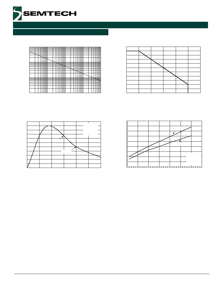
Typical Characteristics
Non-Repetitive Peak Pulse Power vs. Pulse Time
0
10
20
30
40
50
60
70
80
90
100
110
0
25
50
75
100
125
150
Ambient Temperature - T
A
(
o
C)
%
of Rated Power or I
PP
Power Derating Curve
Pulse Waveform
Clamping Voltage vs. Peak Pulse Current
0
10
20
30
40
50
60
70
80
90
100
110
0
5
10
15
20
25
30
Time (
�
s)
Percent of I
PP
e
-t
td = I
PP
/2
Waveform
Parameters:
tr = 8
�
s
td = 20
�
s
0.01
0.1
1
10
0.1
1
10
100
1000
Pulse Duration - tp (
�
s)
Peak Pulse Power - P
PP
(kW)
0
2
4
6
8
10
12
14
16
18
0
5
10
15
20
25
30
35
Peak Pulse Current - I
PP
(A)
Clamping Voltage - V
C
(V)
Pin 2 to 1
Pin 3 to 1
Waveform
Parameters:
tr = 8
�
s
td = 20
�
s
4
� 2000 Semtech Corp.
www.semtech.com
PROTECTION PRODUCTS
PROTECTION PRODUCTS
SLVU2.8
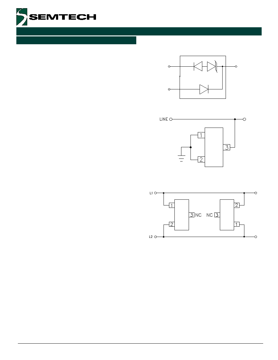
SLVU2.8 Circuit Diagram
Protection of one unidirectional line
Device Connection Options
Electronic equipment is susceptible to transient distur-
bances from a variety of sources including: ESD to an
open connector or interface, direct or nearby lightning
strikes to cables and wires, and charged cables hot
plugged into I/O ports. The SLVU2.8 is designed to
protect sensitive components from damage and latch-
up which may result from such transient events. The
SLVU2.8 can be configured to protect either one
unidirectional line or two (one line pair) high-speed data
lines. The options for connecting the devices are as
follows:
1. Protection of one unidirectional I/O line: Protec-
tion of one data line is achieved by connecting pin
3 to the protected line, and pins 1 and 2 to ground.
This connection option will allow the device to
operate on lines with positive polarity signal transi-
tions (during normal operation). In this configura-
tion, the device adds a maximum loading capaci-
tance of 100pF. During positive duration tran-
sients, the internal TVS diode will be reversed
biased and will act in the avalanche mode, con-
ducting the transient current from pin 3 to 1. The
transient will be clamped at or below the rated
clamping voltage of the device. For negative
duration transients, the internal steering diode is
forward biased, conducting the transient current
from pin 2 to 3. The transient is clamped below
the rated forward voltage drop of the diode.
2. Low capacitance protection of one differential
line pair: Protection of a high-speed differential line
pair is achieved by connecting two devices in anti-
parallel. Pin 1 of the first device is connected to
line 1 and pin 2 is connected to line 2. Pin 2 of the
second device is connected to line 1 and pin 1 is
connected to line 2 as shown. Pin 3 must be left
open on both devices. During negative duration
transients, the first device will conduct from pin 2
to 1. The steering diode conducts in the forward
direction while the TVS will avalanche and conduct
in the reverse direction. During positive transients,
the second device will conduct in the same man-
ner. In this configuration, the total loading capaci-
tance is the sum of the capacitance (between pins
1 and 2) of each device (typically <10pF) making
this configuration suitable for high-speed interfaces
such as 10/100 Ethernet (See application note
SI98-02).
1
2
3
Low capacitance protection of one high-speed line
pair
Circuit Board Layout Recommendations for Suppres-
sion of ESD.
Good circuit board layout is critical for the suppression
of ESD induced transients. The following guidelines are
recommended:
l
Place the SLVU2.8 near the input terminals or
connectors to restrict transient coupling.
l
Minimize the path length between the TVS and the
protected line.
l
Minimize all conductive loops including power and
ground loops.
l
The ESD transient return path to ground should be
kept as short as possible.
l
Never run critical signals near board edges.
l
Use ground planes whenever possible.
Applications Information
5
� 2000 Semtech Corp.
www.semtech.com
PROTECTION PRODUCTS
PROTECTION PRODUCTS
SLVU2.8
Applications Information (continued)
,
PP
,
6%
,
37
,
5
9
5:0
9
9
37
9
&
9
%55
,
%55
6%
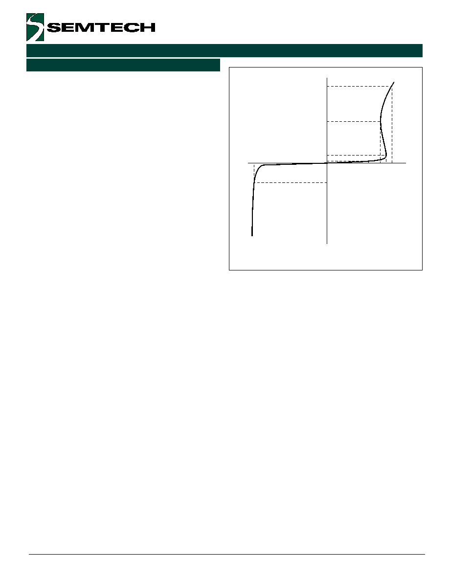
EPD TVS VI Characteristic Curve
EPD TVS
Characteristics
The SLVU2.8 is constructed using Semtechs propri-
etary EPD technology. The structure of the EPD TVS is
vastly different from the traditional pn-junction devices.
At voltages below 5V, high leakage current and junction
capacitance render conventional avalanche technology
impractical for most applications. However, by utilizing
the EPD technology, the SLVU2.8 can effectively
operate at 2.8V while maintaining excellent electrical
characteristics.
The EPD TVS employs a complex nppn structure in
contrast to the pn structure normally found in tradi-
tional silicon-avalanche TVS diodes. The EPD mecha-
nism is achieved by engineering the center region of
the device such that the reverse biased junction does
not avalanche, but will punch-through to a conduct-
ing state. This structure results in a device with supe-
rior dc electrical parameters at low voltages while
maintaining the capability to absorb high transient
currents.
The IV characteristic curve of the EPD device is shown
in Figure 1. The device represents a high impedance
to the circuit up to the working voltage (V
RWM
). During a
transient event, the device will begin to conduct as it is
biased in the reverse direction. When the punch-
through voltage (V
PT
) is exceeded, the device enters a
low impedance state, diverting the transient current
away from the protected circuit. When the device is
conducting current, it will exhibit a slight snap-back or
negative resistance characteristic due to its structure.
This must be considered when connecting the device
to a power supply rail. To return to a non-conducting
state, the current through the device must fall below
the snap-back current (approximately < 50mA).