
1
www.semtech.com
PRELIMINARY
PROTECTION PRODUCTS
SMF05C
TVS Diode Array
For ESD and Latch-Up Protection
Description
Features
Circuit Diagram
Schematic & PIN Configuration
Revision 9/2000
The SMF series TVS arrays are designed to protect sen-
sitive electronics from damage or latch-up due to ESD
and other voltage-induced transient events. They are
designed for use in applications where board space is at
a premium. Each device will protect up to five lines. They
are unidirectional devices and may be used on lines where
the signal polarities are above ground.
TVS diodes are solid-state devices designed specifically
for transient suppression. They feature large cross-sec-
tional area junctions for conducting high transient cur-
rents. They offer desirable characteristics for board level
protection including fast response time, low operating
and clamping voltage, and no device degradation.
The SMF series devices may be used to meet the immu-
nity requirements of IEC 61000-4-2, level 4. The small
SC70 package makes them ideal for use in portable elec-
tronics such as cell phones, PDAs, notebook comput-
ers, and digital cameras.
1
2
3
4
5
6
1
3
4
5
6
2
Applications
Mechanical Characteristics
u
Cellular Handsets & Accessories
u
Cordless Phones
u
Personal Digital Assistants (PDAs)
u
Notebooks & Handhelds
u
Portable Instrumentation
u
Digital Cameras
u
Peripherals
u
MP3 Players
u
ESD protection for data lines to
IEC 61000-4-2 (ESD) 15kV (air), 8kV (contact)
u
Small package for use in portable electronics
u
Protects five I/O lines
u
Working voltage: 5V
u
Low leakage current
u
Low operating and clamping voltages
u
Solid-state silicon-avalanche technology
u
EIAJ SC70-6L package
u
Molding compound flammability rating: UL 94V-0
u
Marking : Marking Code
u
Packaging : Tape and Reel per EIA 481
SC70-6L (Top View)
3
„ 2000 Semtech Corp.
www.semtech.com
PROTECTION PRODUCTS
PRELIMINARY
PROTECTION PRODUCTS
SMF05C
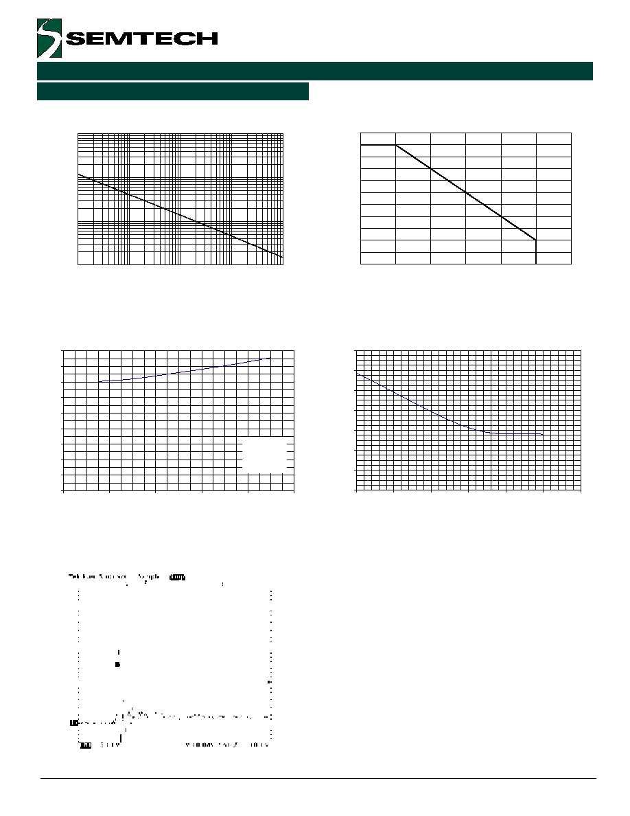
Typical Characteristics
0.01
0.1
1
10
0.1
1
10
100
1000
Pulse Duration - tp (
µ
s)
Peak Pulse Power - P
PP
(kW)
Non-Repetitive Peak Pulse Power vs. Pulse Time
0
10
20
30
40
50
60
70
80
90
100
110
0
25
50
75
100
125
150
Ambient Temperature - T
A
(
o
C)
%
of Rated Power or I
PP
Power Derating Curve
Clamping Voltage vs. Peak Pulse Current
Junction Capacitance vs. Reverse Voltage
ESD Clamping Characteristics
(8kV Contact Discharge per IEC 61000-4-2)
0
20
40
60
80
100
120
140
0
1
2
3
4
5
6
Reverse Voltage (V)
C
a
pacit
a
nce (
pF)
0
1
2
3
4
5
6
7
8
9
0
2
4
6
8
10
Ipp(A)
Vclamp (V)
Waveform
Parameters:
tr = 8
µ
s
td = 20
µ
s

4
„ 2000 Semtech Corp.
www.semtech.com
PRELIMINARY
PROTECTION PRODUCTS
SMF05C
1
3
4
5
6
2
SMF05C Circuit Diagram
Protection of Five Unidirectional Lines
Device Connection for Protection of Five Data Lines
The SMF05C is designed to protect up to five unidirec-
tional data lines. The device is connected as follows:
1. Unidirectional protection of five I/O lines is
achieved by connecting pins 1, 3, 4, 5 and 6 to the
data lines. Pin 2 is connected to ground. The
ground connection should be made directly to the
ground plane for best results. The path length is
kept as short as possible to reduce the effects of
parasitic inductance in the board traces.
Circuit Board Layout Recommendations for Suppres-
sion of ESD.
Good circuit board layout is critical for the suppression
of ESD induced transients. The following guidelines are
recommended:
l
Place the SMF05C near the input terminals or
connectors to restrict transient coupling.
l
Minimize the path length between the SMSxxC and
the protected line.
l
Minimize all conductive loops including power and
ground loops.
l
The ESD transient return path to ground should be
kept as short as possible.
l
Never run critical signals near board edges.
l
Use ground planes whenever possible.
Applications Information

