PROTECTION PRODUCTS
1
www.semtech.com
PROTECTION PRODUCTS - MicroClamp
uClamp0501H
µ
Clamp
TM
1-Line ESD protection
Description
Features
Dimensions
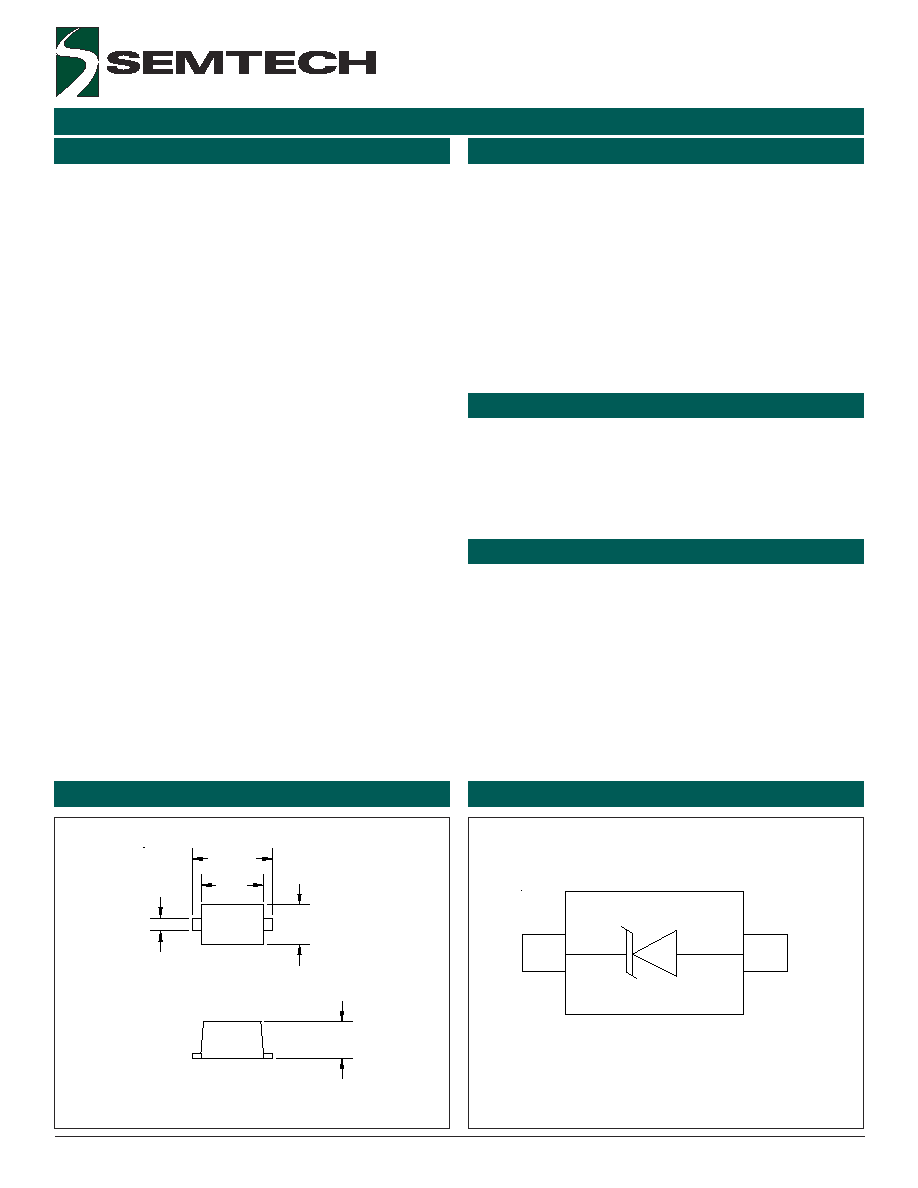
Schematic & PIN Configuration
Revision 10/08/2003
The
µ
Clamp
TM
series of TVS arrays are designed to protect
sensitive electronics from damage or latch-up due to ESD.
It is designed to replace multilayer varistors (MLVs) in por-
table applications such as cell phones, notebook comput-
ers, and PDA's. It features large cross-sectional area junc-
tions for conducting high transient currents. It offers su-
perior electrical characteristics such as lower clamping volt-
age and no device degradation when compared to MLVs.
They offer desirable characteristics for board level protec-
tion including fast response time, low operating and clamp-
ing voltage, and no device degradation.
The
µ
clamp
TM
0501H is in a ultra-small SOD-523 pack-
age ideal for use in portable electronics such as cell
phones, PDA's, notebook computers, and digital
cameras. It will protect one unidirectional line operat-
ing at 5 volts. It gives the designer the flexibility to
protect one line in applications where arrays are not
practical. Additionally, it may be "sprinkled" around the
board in applications where board space is at a pre-
mium.
This device may be used to meet the ESD immunity
requirements of IEC 61000-4-2, Level 4 (15kV air, 8kV
contact discharge).
Applications
Mechanical Characteristics
!
Cellular Handsets & Accessories
!
Cordless Phones
!
Personal Digital Assistants (PDA's)
!
Notebooks & Handhelds
!
Portable Instrumentation
!
Digital Cameras
!
Peripherals
!
MP3 Players
!
Transient protection for data lines to
IEC 61000-4-2 (ESD) 15kV (air), 8kV (contact)
IEC 61000-4-4 (EFT) 40A (tp = 5/50ns)
Cable Discharge Event (CDE)
!
Ultra-small SOD-523 package (1.7 x 0.9 x 0.7mm)
!
Protects one I/O or power line
!
Low clamping voltage
!
Working voltage: 5V
!
Low leakage current
!
Solid-state silicon-avalanche technology
!
EIAJ SOD-523 package
!
Molding compound flammability rating: UL 94V-0
!
Marking : Marking code, cathode band
!
Packaging : Tape and Reel per EIA 481
!
Lead Finish: Matte tin
SOD-523 (Top View)
0.9
1.70
1.30
0.35
0.70
Maximum Dimensions (mm)
3
2003 Semtech Corp.
www.semtech.com
PROTECTION PRODUCTS
uClamp0501H
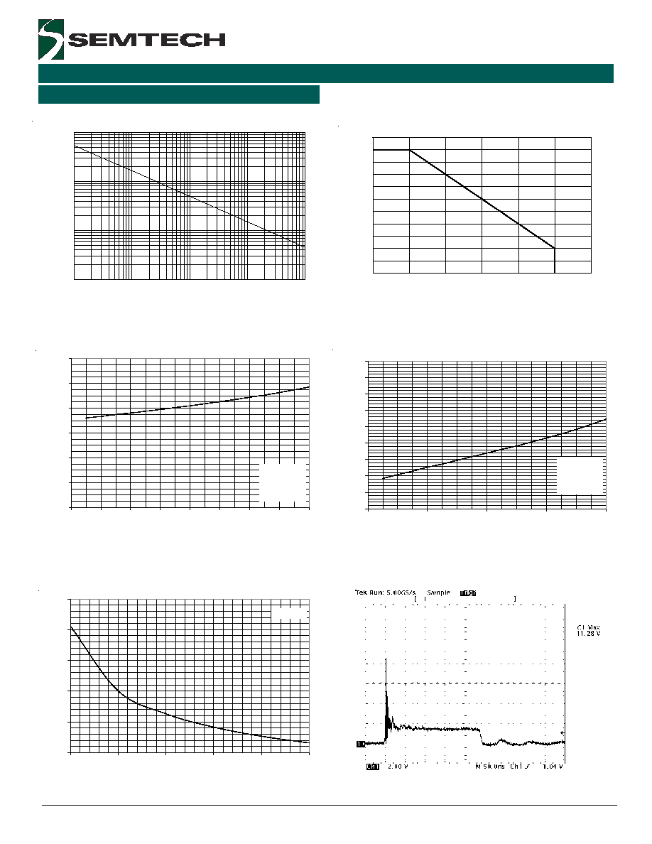
Typical Characteristics
Non-Repetitive Peak Pulse Power vs. Pulse Time
0
10
20
30
40
50
60
70
80
90
100
110
0
25
50
75
100
125
150
Ambient Temperature - T
A
(
o
C)
%
of Rated Power or I
PP
Power Derating Curve
Clamping Voltage vs. Peak Pulse Current
Forward Voltage vs. Forward Current
Junction Capacitance vs. Reverse Voltage
ESD Clamping
(8kV Contact per IEC 61000-4-2)
0.01
0.1
1
10
0.1
1
10
100
1000
Pulse Duration - t
p
(µs)
P
eak
P
u
l
s
e P
o
w
e
r -
P
pk
(kW
)
0
0.5
1
1.5
2
2.5
3
3.5
4
4.5
0
4
8
12
16
Forward Current - I
F
(A)
F
o
r
w
ar
d
V
o
lt
ag
e - V
F
(V
)
Waveform
Parameters:
tr = 8µs
td = 20µs
60
80
100
120
140
160
0
1
2
3
4
5
Reverse Voltage - V
R
(V)
Cap
aci
tance -
C
j
(
pF)
f = 1 MHz
0
2
4
6
8
10
12
0
2
4
6
8
10
12
14
16
Peak Pulse Current - I
PP
(A)
C
l
am
pi
ng
Vol
t
a
g
e
-
V
C
(V
)
Waveform
Parameters:
tr = 8µs
td = 20µs
4
2003 Semtech Corp.
www.semtech.com
PROTECTION PRODUCTS
uClamp0501H
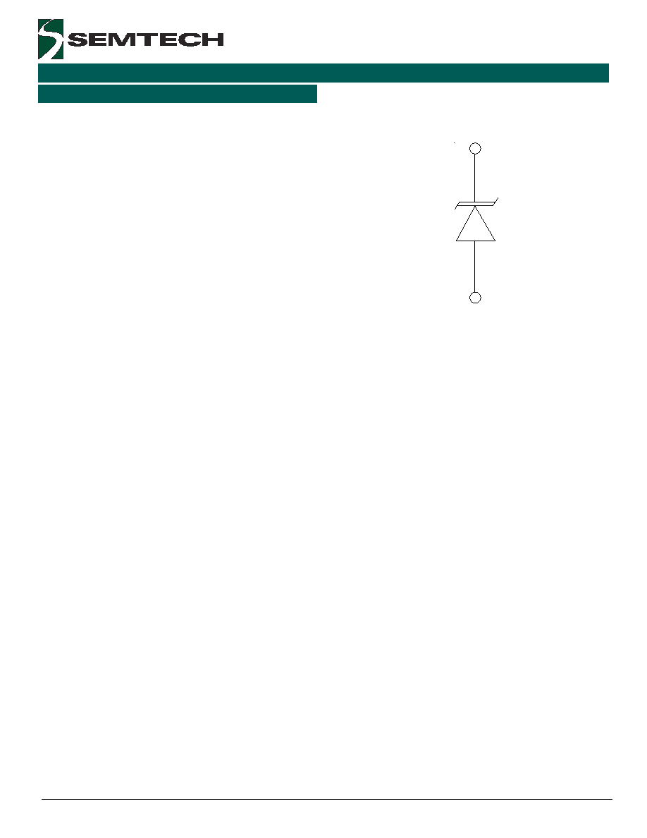
Circuit Diagram
Device Connection Options
These TVS diodes are designed to protect one data, I/
O, or power supply line. The device is unidirectional
and may be used on lines where the signal polarity is
above ground. The cathode band should be placed
towards the line that is to be protected.
Circuit Board Layout Recommendations for Suppres-
sion of ESD.
Good circuit board layout is critical for the suppression
of ESD induced transients. The following guidelines are
recommended:
"
Place the TVS near the input terminals or connec-
tors to restrict transient coupling.
"
Minimize the path length between the TVS and the
protected line.
"
Minimize all conductive loops including power and
ground loops.
"
The ESD transient return path to ground should be
kept as short as possible.
"
Never run critical signals near board edges.
"
Use ground planes whenever possible.
Matte Tin Lead Finish
Matte tin has become the industry standard lead-free
replacement for SnPb lead finishes. A matte tin finish
is composed of 100% tin solder with large grains.
Since the solder volume on the leads is small com-
pared to the solder paste volume that is placed on the
land pattern of the PCB, the reflow profile will be
determined by the requirements of the solder paste.
Therefore, these devices are compatible with both
lead-free and SnPb assembly techniques. In addition,
unlike other lead-free compositions, matte tin does not
have any added alloys that can cause degradation of
the solder joint.
Applications Information

