 | –≠–ª–µ–∫—Ç—Ä–æ–Ω–Ω—ã–π –∫–æ–º–ø–æ–Ω–µ–Ω—Ç: 6N135 | –°–∫–∞—á–∞—Ç—å:  PDF PDF  ZIP ZIP |
6N135/6N136
6N135/6N136
General Purpose Type
Photocoupler
*1 50% duty cycle, Pulse width : 1ms
*2 Pulse width<=1
µ
s, 300
P
/
S
*4 For 10 seconds
Decreases at the rate of 1.6mA/∞C if the external temperature is 70∞C or more.
s
Features
1. High speed response t
PHL
, t
PLH
2. High common mode rejection voltage
3. Standard dual-in-line package
s
Applications
2. High speed line receivers, high speed logic
3. Telephone sets
4. Signal transmission between circuits of
different potentials and impedances
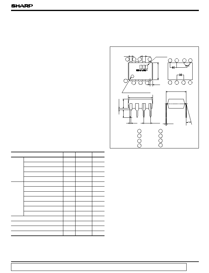
6N
Model
Internal
connection
diagram
s
Outline Dimensions
s
Absolute Maximum Ratings
( Ta = 25∞C)
( Unit : mm)
Parameter Symbol Rating Unit
Input
Forward current I
F
25 mA
*1
Peak forward current I
F
50 mA
*2Peak transient
forward current
I
FM
1
A
Reverse voltage V
R
5
V
Power dissipation P 45 mW
Output
Supply voltage V
CC
- 0.5 to + 15 V
Output voltage V
O
- 0.5 to + 15 V
Emitter-base reverse with-
V
EBO
5
V
Average output current I
O
8
mA
Peak output current I
OP
16 mA
Base current ( Pin 7 ) I
B
5
mA
Power dissipation P
O
100 mW
*3
Isolation voltage V
iso
Operating temperature T
opr
- 55 to + 100 ∞C
Storage temperature T
stg
- 55 to + 125 ∞C
*4
Soldering temperature T
so1
260 ∞C
( CM
H
: TYP. 1kV/
µ
s )
(
6N135
: MAX. 1.5
µ
s at R
L
= 4.1k
)
(
6N136
: MAX. 0.8
µ
s at R
L
= 1.9k
)
data books, etc. Contact SHARP in order to obtain the latest version of the device specification sheets before using any SHARP's device.
"
"
In the absence of confirmation by device specification sheets, SHARP takes no responsibility for any defects that occur in equipment using any of SHARP's devices, shown in catalogs,
equipment
stand voltage ( Pin 5 to 7
)
No.
0.8
0.5TYP
1
2
3
4
5
6
7
8
1
2
3
4
5
6
7
8
1 NC
2 Anode
3 Cathode
4 NC
5 GND
4. Recognized by UL, file No. E64380
1. Computers, measuring instruments, control
An OPIC consists of a light-detecting element and signal-
processing circuit integrated onto a single chip.
* " OPIC " ( Optical IC ) is a trademark of the SHARP Corporation.
2 500
*3 40 to 60% RH, AC for 1 minute
Primary side mark
(Sunken place )
V
rms
=
0 to 13
∞
6 V
O
7 V
B
8 V
CC
6.5
±
0.5
1.2
±
0.3
0.85
±
0.3
9.22
±
0.5
7.62
±
0.3
3.5
±
0.5
3.7
±
0.5
0.5
±
0.1
2.54
±
0.25
0.26
±
0.1

6N135/6N136
*5 Current transfer ratio is the ratio of input current and output
current expressed in % .
*6 Measured as 2-pin element ( Short 1, 2, 3, 4 )
s
Electro-optical Characteristics
Parameter
Symbol
Conditions
MIN.
TYP.
MAX.
Unit
*5
Current transfer
ratio
6N135
CTR(1)
Ta = 25 ∞C, I
F
= 16mA
V
O
= 0.4V, V
CC
= 4.5V
7.0
40
-
%
6N136
CTR(1)
19
40
-
%
6N135
CTR(2)
I
F
= 16mA, V
O
= 0.5V
V
CC
= 4.5V
5.0
43
-
%
6N136
CTR(2)
15
43
-
%
Logic ( 0) output voltage
V
OL
I
F
= 16mA, V
CC
= 4.5V
-
0.1
0.4
V
Logic ( 1) output current
I
OH
(1)
T
a
= 25 ∞C, I
F
= 0
V
CC
= V
O
= 5.5V
-
3.0
500
nA
I
OH
(2)
T
a
= 25 ∞C, I
F
= 0
V
CC
= V
O
= 15V
-
0.01
1.0
A
I
OH
(3)
I
F
= 0, V
CC
= V
O
= 15V
-
-
50
A
Logic ( 0) supply current
I
CCL
I
F
= 16mA, V
CC
= 15V
V
O
= open
-
200
-
A
Logic ( 1) supply current
I
CCH
(1)
T
a
= 25 ∞C, V
CC
= 15V
V
F
= open, I
O
= 0
-
0.02
1.0
A
I
CCH
(2)
V
CC
= 15V
V
O
= open, I
F
= 0
-
-
2.0
A
Input forward voltage
V
F
T
a
= 25 ∞C, I
F
= 16mA
-
1.7
1.95
V
Input forward voltage
V
F
/
T
a
I
F
= 16mA
-
- 1.9
-
mV/ ∞C
Input reverse voltage
BV
R
T
a
= 25 ∞C, I
R
= 10
A
5.0
-
-
V
Input capacitance
C
IN
V
F
= 0, f = 1MHz
-
60
-
I
I-O
T
a
V
I-O
= 3kVDC
-
-
1.0
A
R
I-O
V
I-O
= 500VDC
-
10
12
-
C
I-O
f = 1MHz
-
0.6
-
h
FE
V
O
= 5V, I
O
= 3mA
-
70
-
*7
6N135
: I
O
= 1.1mA,
6N136
: I
O
= 2.4mA
( Ta = 0 to + 70 ∞C unless otherwise specified )
temperature coefficient
Note ) Typical volue : at Ta = 25 ∞C
*6
Leak current
(input-output )
*6
Isolation resistance
(input-output )
*6
Capacitance ( input-output )
Transistor current
amplification factor
*7
= 25 ∞C, 45 % RH, t = 5s
pF
pF
µ
µ
µ
µ
µ
µ
µ
6N135/6N136
*13 Bandwidth represents a point where AC input goes down by 3dB.
Instantaneous common mode rejection voltage " output ( 0) " represents a common
mode voltage variation that can hold the output above
( 0) level ( V
O
< 0.8V).
*8 R
L
L
= 4.1k
is equivalent to one LSTTL and 6.1k
pull-up resistor. R =1.9k
is equivalent to one TTL and 5.6k
pull-up resistor.
Symbol
Conditions
MIN.
TYP.
MAX.
Unit
t
PHL
R
L
= 4.1k
-
0.3
1.5
s
t
PHL
R
L
= 1.9k
-
0.3
0.8
s
t
PLH
R
L
= 4.1k
-
0.4
1.5
s
t
PLH
R
L
= 1.9k
-
0.3
0.8
s
CM
H
-
-
V/
s
CM
L
-
-
V/
s
BW
R
L
= 100
-
2.0
-
MHz
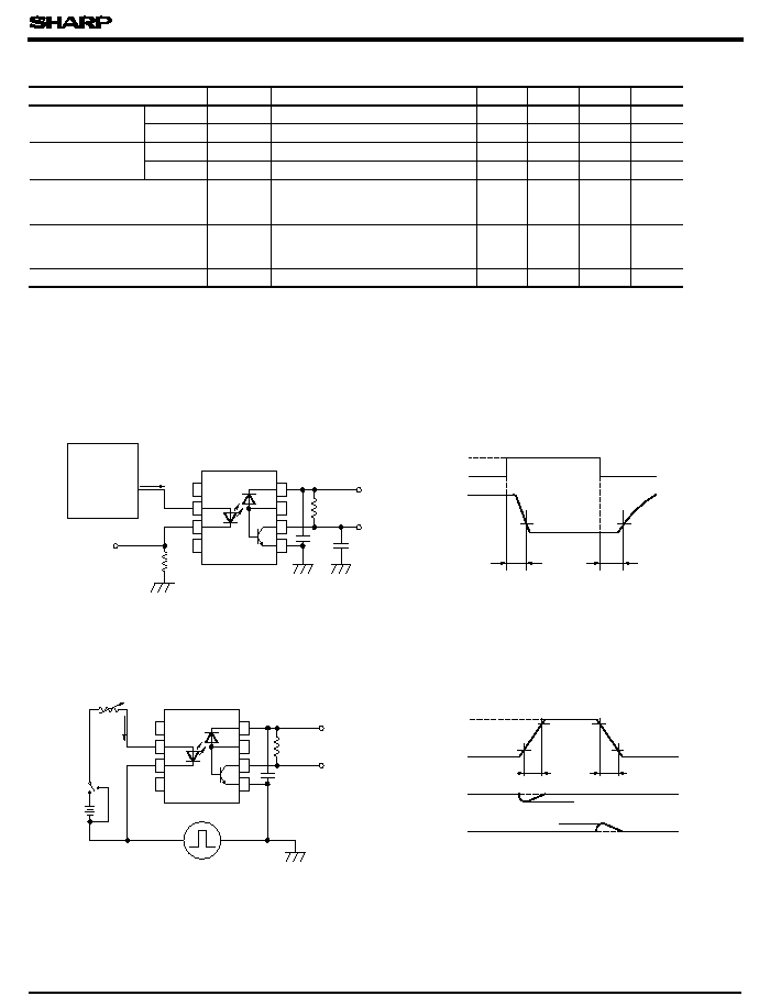
Pulse
Generator
100
Pulse input
Duty ratio
1
2
3
4
8
7
6
5
1.5V
1.5V
5V
5
6
7
8
4
3
2
1
+
-
A
B
10V
0V
2V
0.8V
10
%
90
%
10
%
90
%
=
1/10
I
F
I
F
monitor
C
L
=
15pF
0.01
µ
F
V
O
V
CC
R
L
I
F
0
V
O
t
PHL
t
PLH
V
FF
I
F
V
CM
R
L
V
O
V
CM
CM
H
V
O
CM
L
V
O
I
F
=
16mA
I
F
=
0
5V
V
OL
t
r
t
f
*12
I
F
= 0, V
CM
= 10V
P-P
*12
V
CM
= 10V
P-P
, I
F
= 16mA
s
Switching Characteristics
(Ta = 25 ∞C, V
CC
= 5V, I
F
= 16mA )
*10 Instantaneous common mode rejection voltage " output ( 1) " represents a common
mode voltage variation that can hold the output above
( 1) level ( V
O
> 2.0V).
Parameter
Output (1)
(0)
6N135
6N136
Output (0)
(1)
6N135
6N136
*10,11
Instantaneous common
mode rejection voltage
" output ( 1) "
*10,11
Instantaneous common
mode rejection voltage
" output ( 0) "
*13
Bandwidth
*12
6N135
: R
L
= 4.1k
6N136
: R
L
= 1.9k
*8
Propagation
*9
delay time
*8
Propagation
*9
delay time
*11 Test Circuit for Instantaneous Common Mode Rejection Voltage
V
CC
=
5V
1 000
- 1 000
*9 Test Circuit for Propagation Delay Time
0.01
µ
F
µ
µ
µ
µ
µ
µ

5
10
30
25
20
15
0
125
100
75
50
25
0
- 55
Ambient Temperature
Ambient temperature T
a
(∞C)
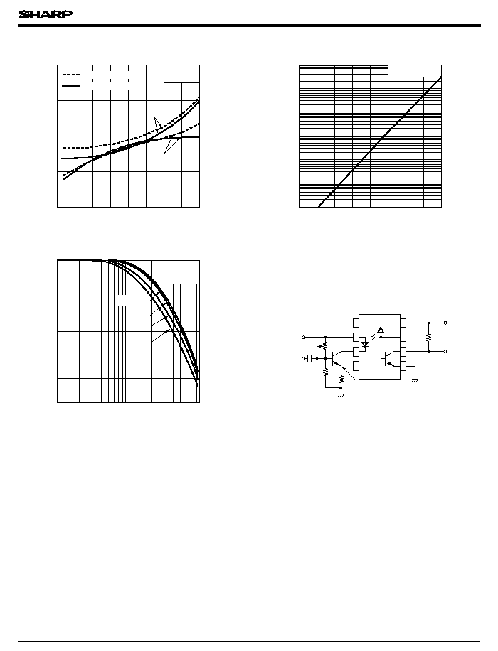
Fig. 1 Forward Current vs.
F
(
mA
)
0
120
-40
P
0
25
50
75
100
125
100
80
60
20
40
70
45
Fig. 2 Power Dissipation vs.
Ambient Temperature
Power dissipation P, P
O
(
mW
)
Ambient temperature T
a
(∞C)
50∞C
25∞C
70∞C
1.0
0.01
0.1
1
10
100
1.2
1.4
1.6
1.8
2.0
2.2
F
(
mA
)
Forward voltage V
F
(V)
Forward Voltage
Fig. 3 Forward Current vs.
0
0.1
CTR = 100% at
50
100
150
1
10
100
Forward Current
Forward current I
F
( mA )
Fig. 4 Relative Current Transfer Ratio vs.
0
0
2
2
Dotted line shows
4
6
8
10
12
14
16
18
20
4
6
8
10
12
14
pulse characteristics
20mA
15mA
10mA
5mA
20
16
18
Output current I
O
(
mA
)
Output voltage V
O
(V)
Fig. 5 Output Current vs. Output Voltage
80
60
70
90
100
110
0
20
40
60
80
100
Relative current transfer ratio
(
%
)
Ambient Temperature
Fig. 6 Relative Current Transfer Ratio vs.
Ambient temperature T
a
(∞C)
Forward current I
Forward current I
- 60
- 40
- 20
Relative current transfer ratio
(
%
)
P
O
T
a
= 0∞C
I
F
= 16mA
T
a
= 25 ∞C
V
O
= 0.4V
V
CC
= 5V
T
a
= 25 ∞C
V
CC
= 5V
I
F
= 25mA
I
F
= 16mA
V
O
= 0.4V
V
CC
= 5V
CTR = 100 % at T
a
= 25 ∞C
6N135/6N136
0
200
400
600
800
- 60
- 20
20
60
100
80
40
0
- 40
Ambient Temperature
Fig. 7 Propagation Delay Time vs.
PHL
, t
PLH
(
ns
)
Ambient temperature T
a
(∞C)
- 60
- 40
- 20
0
20
100
80
60
40
V
CC
= V
O
= 5V
Ambient Temperature
Ambient temperature T
a
(∞C)
10
- 5
10
- 6
10
- 7
10
- 8
10
- 9
10
- 10
10
- 11
High level output current I
OH
(
A
)
Fig. 8 High Level Output Current vs.
Frequency f ( MHz )
-20
-15
-10
-5
0
-25
-30
0.1
0.2
0.5
1
2
5
10
220
470
1k
Fig. 9 Frequency Response
Voltage gain A
V
(
dB
)
I
F
= 16mA
T
a
= 25∞C
R
L
= 100
Propagation delay time t
100
15V
V
O
560
AC
Input
20k
R
L
1.6V DC
0.25V
AC
5V
1
2
3
4
8
7
6
5
( 1) It is recommended that a by-pass capacitor of more than 0.01 F be added between V
CC
and
GND near the device in order to stabilize power supply line.
( 2) Transistor of detector side in bipolar configuration is apt to be affected by static electricity
for its minute design. When handling them, general counterplan against static electricity
should be taken to avoid breakdown of devices or degradation of characteristics.
s
Precautions for Use
6N135/6N136
Test Circuit for Frequency Characteristic
V
CC
= 5V
I
F
= 16mA
t
PLH
t
PHL
( Page 78 to 93 )
P P
-
6N136 (R
L
=
1.9k
)
6N135 (R
L
=
4.1k
)
As for other general cautions, please refer to the chapter " Precautions for Use " .
µ
q