 | –≠–ª–µ–∫—Ç—Ä–æ–Ω–Ω—ã–π –∫–æ–º–ø–æ–Ω–µ–Ω—Ç: 6N137 | –°–∫–∞—á–∞—Ç—å:  PDF PDF  ZIP ZIP |

6N137
s
Features
s
Applications
s
Outline Dimensions
(Ta = 25∞C)
6N137
2. Isolation voltage between input and output
5. LSTTL and TTL compatible output
4. Instantaneous common mode rejection
voltage
1. High speed interfaces for computer
peripherals, microcomputer systems
2. High speed line receivers
3. Noise reduction
s
Absolute Maximum Ratings
*3 For 1 minute MAX.
*4 Not exceed 500mV or more than
*5 AC for 1 minute, 40 to 60% RH
Apply the specific voltage between all the input
electrode pins connected together and all the
output electrode pins connected together.
*6 2mm or more away from the lead base for 10
seconds
6N137
1
4
2
3
6
7
5
8
Internal connection
diagram
1.2
1 NC
2 Anode
3 Cathode
4 NC
8 V
7 V
6 V
5 GND
O
E
CC
( t
PHL
, t
PLH
: TYP. 45ns at R
L
= 350
)
V
3. Low input current drive ( I
FHL
1
4
2
3
6
7
5
8
0.5TYP
data books, etc. Contact SHARP in order to obtain the latest version of the device specification sheets before using any SHARP's device.
"
"
In the absence of confirmation by device specification sheets, SHARP takes no responsibility for any defects that occur in equipment using any of SHARP's devices, shown in catalogs,
CM
H
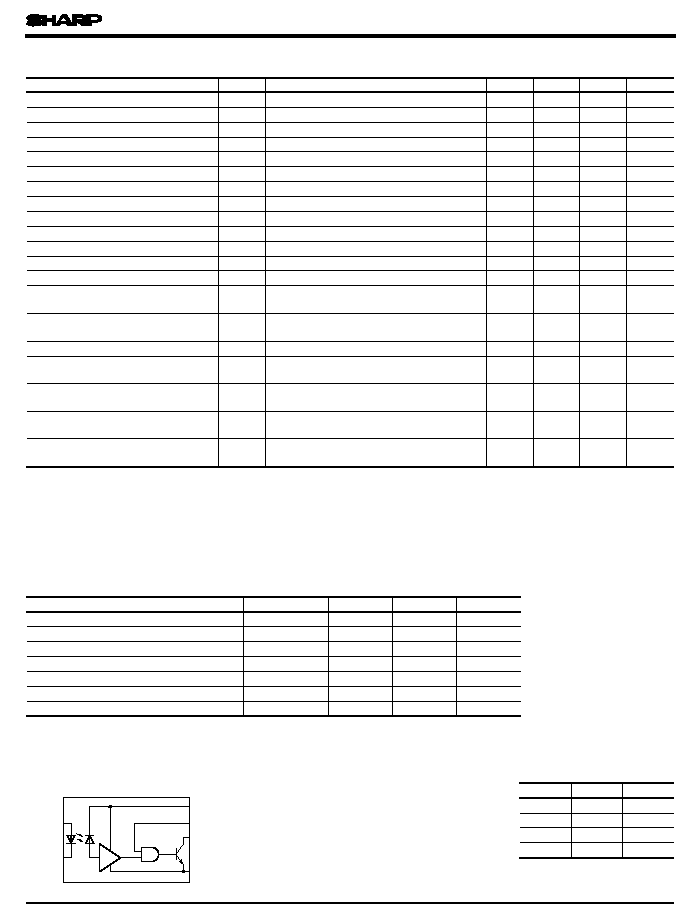
OPIC Photocoupler
An OPIC consists of a light-detecting element and signal-
processing circuit integrated onto a single chip.
* " OPIC " ( Optical IC ) is a trademark of the SHARP Corporation.
Super High Speed Response
1. Super high speed response
iso
: MAX. 5mA )
: TYP. 500V /
s
4. Interfaces for data transmission equipment
*1 Ta = 0 to 70 ∞C
*2 Pulse width <= 1ms
supply voltage ( V
CC
)
Parameter
Input
Reverse voltage
Output
Supply voltage
Enable voltage
High level output voltage
Low level output current
Output collector
power dissipation
Operating temperature
Storage temperature
*1
Forward current
*2
Peak forward current
*6
Soldering temperature
*5
Isolation voltage
Rating
Unit
20
mA
40
mA
5
V
7
V
5.5
V
7
V
50
mA
85
mW
0 to + 70
∞C
- 55 to + 125
∞C
260
∞C
Symbol
I
F
I
FM
V
R
V
CC
C
E
V
OIL
I
OL
P
C
V
iso
T
opr
T
stg
T
sol
( Unit : mm)
2 500
Primary side mark ( Sunken place )
: 2 500V
rms
V
rms
0.85
±
0.3
6.5
±
0.5
0.8
±
0.2
1.2
±
0.3
7.62
±
0.3
0.26
±
0.1
2.54
±
0.25
0.5
±
0.1
3.7
±
0.5
3.5
±
0.5
9.22
±
0.5
=
0 to 13
∞
6. Recognized by UL , file No. E64380
µ
6N137
s
Electro-optical Characteristics
Note ) Typical values are all at V
CC
= 5V, Ta = 25∞C
*1 Measured as 2-pin element. Connect pins 2 and 3, connect pins 5, 6, 7 and 8.
*2 At I
in
= 10 mA, V
F
decreases at the rate of 1.6mV/∞C if the temperature goes up.
*3 DC current transfer ratio is defined as the ratio of output collector current to forward bias input current.
*4, *5 Refer to the Fig. 1.
*6, *7 Refer to the Fig. 2.
*8 CM
H
represents a common mode voltage ignorable rise time ratio that can hold logic ( 1) state in output.
CM
L
represents a common mode voltage ignorable fall time ratio that can hold logic ( 0) state in output.
s
Recommmended Operating Conditions
L:Logic ( 0 ) H:Logic ( 1 )
Truth Table
1. No necessary external pull-up resistor to hold enable input at high level
2. Connect a ceramic by-pass capacitor ( 0.01 to 0.1
F ) between V
CC
and GND at the position within 1cm from pin.
Anode
Cathode
V
V
V
GND
O
E
CC
(Enable)
Circuit Block Diagram
Input
Enable
Output
H
H
L
L
H
H
H
L
H
L
L
H
Parameter
Symbol
MIN.
MAX.
Unit
Low level input current
I
FL
0
250
A
High level input current
I
FH
7.0
15
mA
High level enable voltage
V
EH
2.0
V
CC
V
Low level enable voltage
V
EL
0
0.8
V
Supply voltage
V
CC
4.5
5.5
V
Fanout ( TTL load )
N
-
8
Operating temperature
T
opr
0
70
∞C
Parameter
Symbol
Conditions
MIN.
TYP.
MAX.
Unit
Logic ( 1) output current
I
OH
V
CC
= 5.5V, V
O
= 5.5V, I
F
= 250
µ
A, V
E
= 2.0V
-
2
250
A
Logic ( 0) output voltage
V
OL
V
CC
= 5.5V, I
F
EH
= 2.0V, I
OL
-
0.4
0.6
V
Logic ( 1) enable current
I
EH
V
CC
= 5.5V, V
E
= 2.0V
-
- 0.8
-
Logic ( 0) enable current
I
EL
V
CC
= 5.5V, V
E
= 0.5V
-
- 1.2
- 2.0
Logic ( 1) supply current
I
CCH
V
CC
= 5.5V, I
F
E
= 0.5V
-
7
15
Logic ( 0) supply current
I
CCL
V
CC
= 5.5V, I
F
E
= 0.5V
-
13
18
*1
Leak current
I
I-O
I-O
dc
-
-
1.0
m A
*1
Isolation resistance
( input-output )
R
I-O
V
I-O
= 500V, Ta = 25∞C
-
10
12
-
*1
Capacitance ( input-output )
C
I-O
f = 1MHz, Ta = 25∞C
-
0.6
-
pF
*2
Input forward voltage
V
F
I
F
-
1.6
1.75
V
Input reverse voltage
BV
R
I
R
= 10 m A, Ta = 25∞C
5
-
-
V
Input capacitance
C
IN
V
F
= 0, f = 1MHz
-
60
-
pF
*3
Current transfer ratio
CTR
I
F
L
= 100
-
700
-
%
*4
Propagation delay time
Output ( 0)
(1)
t
PLH
Ta = 25∞C, V
CC
= 5V, R
L
= 350
, C
L
= 15pF, I
F
-
45
75
ns
*5
Propagation delay time
Output (1)
( 0)
t
PHL
Ta = 25∞C, V
CC
= 5V, R
L
= 350
, C
L
= 15pF, I
F
-
45
75
ns
t
r
, t
f
R
L
= 350
, C
L
= 15pF, I
F
-
20, 30
-
ns
*6
Enable propagation
delay time (1)
( 0)
t
ELH
R
L
= 350
, C
L
= 15pF, I
F
EH
= 3.0V, V
EL
= 0.5V
-
40
-
ns
*7
Enable propagation
delay time
( 0)
(1)
t
EHL
R
L
= 350
, C
L
= 15pF, I
F
EH
= 3.0V, V
EL
= 0.5V
-
15
-
ns
*8
Instantaneous common mode
rejection voltage " Output ( 0) "
CM
H
V
CM
= 10V, R
L
= 350
, V
O
F
-
500
-
V/
s
*8
Instantaneous common mode
rejection voltage " Output (1) "
CM
L
V
CM
= 10V, R
L
= 350
, V
O
F
-
- 500
-
V/
s
Output rise-fall time
( 10 to 90% )
mA
mA
mA
mA
= 5mA, V
(Sinking ) = 13mA
= 0mA, V
= 10mA, V
= 7.5mA
= 7.5mA
= 10mA, Ta = 25∞C
= 5.0mA, R
= 5mA
= 0mA
( min. ) = 2V, I
(max. ) = 0.8V, I
= 7.5mA, V
= 7.5mA, V
= 7.5mA
( Ta = 0 to + 70∞C unless otherwise specified )
45% RH, Ta = 25∞C, t = 5s, V = 3 000V
-
µ
µ
µ
µ
µ

Fig.1 Test Circuit for Propagation Delay time
Fig.2 Test Circuit for Enable Propagation Delay Time
Fig.3 Test Circuit for Instantaneous Common Mode
Rejection Voltage
+
5V
GND
R
V
OUT
L
CC
8
7
6
5
3
4
2
1
V
R
t
=
5ns
Z
O
=
50
oscillator
Pulse
I
F
F
I
47
Input
detection
C
L
Output
detection
0.1
µ
F
Bypass
350mV ( I
F
=
7.5mA)
=
3.75mA)
F
t
PLH
t
V
OH
OL
V
1.5V
Input
in
I
V
out
Output
L
C
Input
detection
F
I
Pulse
oscillator
=
50
O
Z
=
5ns
t
R
V
1
2
4
3
5
6
7
8
CC
L
O
V
R
GND
+
5V
0.1
µ
F
Bypass
V
E
=
7.5mA
3V
1.5V
V
E
Input
Output
V
out
OH
V
V
1.5V
OL
t
t
+
5V
GND
R
V
O
L
CC
8
7
6
5
3
4
2
1
V
I
F
B
A
Bypass
0.1
µ
F
+
-
CM
V
Z
O
=
50
Pulse oscillator
10V
V
OL
0V
(I
F
=
5mA)
=
0mA)
F
(I
CM
V
V
O
O
V
f
t
90
%
10
%
90
%
10
%
5V
at SW
=
A
at SW
=
B
10
20
100
40
30
0
0
25
70
75
100
50
60
70
80
90
85
Collector power dissipation P
C
(
mW
)
Ambient temperature T
a
(∞C)
50∞C
25∞C
70∞C
1.0
0.01
0.1
1
10
100
1.2
1.4
1.6
1.8
2.0
2.2
F
Forward voltage V
F
(V)
Forward current I
175mV (I
PHL
EHL
ELH
t
r
6N137
(
mA
)
T
a
= 0∞C
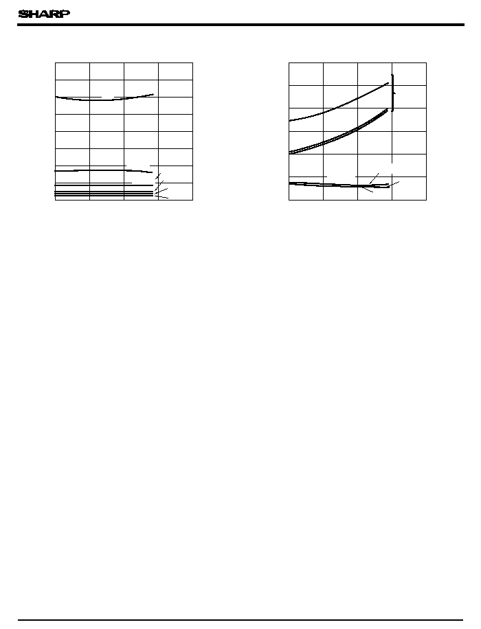
Fig. 4 Output Collector Power Dissipation vs.
Ambient Temperature
Fig. 5 Forward Current vs. Forward Voltage

6N137
2
3
4
0
25
50
75
100
1
0
Ambient Temperature
High level output current I
OH
(
µ
A
)
Ambient temperature T
a
(∞C)
Fig. 6 High Level Output Current vs.
0.2
0.3
0.5
0
25
50
100
0.1
0.4
75
12.8mA
9.6mA
6.4mA
Ambient Temperature
Ambient temperature T
a
(∞C)
Low level output voltage V
OL
(
V
)
Fig. 7 Low Level Output Voltage vs.
0
1
2
6
0
3
1
2
6
4
3
1k
5
4
5
4k
Output Voltage V
O
(
V
)
Forward current I
F
( mA )
0
1
2
6
0
3
1
2
6
4
3
5
4
5
(Ambient Temp. Characteristics )
Output Voltage V
O
(
V
)
Forward current I
F
( mA )
0
20
40
60
100
120
10
15
20
5
80
1k
350
1k
4k
Forward Current
Fig. 9 Propagation Delay Time vs.
Forward current I
F
( mA )
20
40
60
80
100
120
0
25
50
75
100
1k
350
1k
4k
Ambient Temperature
Ambient temperature T
a
(∞C)
Fig.10 Propagation Delay Time vs.
Propagation delay time t
PHL
, t
PLH
(
ns
)
Propagation delay time t
PHL
, t
PLH
(
ns
)
Fig. 8-a Output Voltage vs. Forward Current
T
a
= 0 to 70∞C
Fig. 8-b Output Voltage vs. Forward Current
I
F
= 250
A
V
O
= 5.5VC
V
E
= 2V
V
CC
= 5.5V
V
E
= 2V
V
CC
= 5.5V
I
F
= 5mA
I
O
= 16mA
T
a
= 25∞C
V
CC
= 5V
R
L
= 350
V
CC
= 5V
T
a
= 0 to 70∞C
R
L
= 350
R
L
= 1k
R
L
= 4k
T
a
= 25∞C
V
CC
= 5V
R
L
= 350
t
PHL
t
PLH
t
PLH
t
PLH
V
CC
= 5V
I
F
= 7.5mA
t
PLH
R
L
= 4k
t
PHL
R
L
= 350
µ
6N137
0
40
50
100
75
25
80
120
160
200
240
280
320
1k
1k
4k
350
Ambient Temperature
Ambient temperature T
a
(∞C)
Rise time, fall time t
r
, t
f
(
ns
)
Fig.11 Rise Time, Fall Time vs.
20
50
100
75
25
40
60
80
100
120
1k
4k
1k
350
0
0
Ambient Temperature
, t
ELH
(
ns
)
Ambient temperature T
a
(∞C)
Fig.12 Enable Propagation Time vs.
s
Precautions for Use
}
EHL
Enable propagation time t
V
CC
= 5V
I
F
= 7.5mA
V
CC
= 5V
I
F
= 7.5mA
R
L
= 4k
t
r
t
f
t
r
R
L
= 350
R
L
= 4
k
R
L
= 350
t
EHL
t
ELH
Handle this product the same as with other integrated circuits against static electricity.
Please refer to the chapter " Precautions for Use " .
q
q