LH540235/45
2048
◊
18 / 4096
◊
18 Synchronous FIFOs
FEATURES
∑
Fast Cycle Times: 20/25/35 ns
∑
Pin-Compatible Drop-In Replacements for
IDT72235B/45B FIFOs
∑
Choice of IDT-Compatible or
Enhanced
Operating
Mode; Selected by an Input Control Signal
∑
Device Comes Up into One of Two Known Default
States at Reset Depending on the State of the
EMODE
Control Input: Programming is Allowed, but
is not Required
∑
Internal Memory Array Architecture Based on CMOS
Dual-Port SRAM Technology, 2048
◊
18 or 4096
◊
18
∑
`Synchronous' Enable-Plus-Clock Control at Both
Input Port and Output Port
∑
Independently-Synchronized Operation of Input Port
and Output Port
∑
Control Inputs Sampled on Rising Clock Edge
∑
Most Control Signals Assertive-LOW for
Noise Immunity
∑
May be Cascaded for Increased Depth, or
Paralleled for Increased Width
∑
16 mA-IOL High-Drive Three-State Outputs
∑
Five Status Flags: Full, Almost-Full, Half-Full,
Almost-Empty, and Empty; `Almost' Flags are
Programmable
∑
In Enhanced Operating Mode, Almost-Full,
Half-Full, and Almost-Empty Flags can be Made
Completely Synchronous
∑
In Enhanced Operating Mode, Duplicate Enables
for Interlocked Paralleled FIFO Operation, for
36-Bit Data Width, when Selected and
Appropriately Connected
∑
In Enhanced Operating Mode, Disabling
Three-State Outputs May be Made to Suppress
Reading
∑
Data Retransmit Function
∑
TTL/CMOS-Compatible I/O
∑
Space-Saving 68-Pin PLCC Package; Even-Smaller
64-Pin TQFP Package
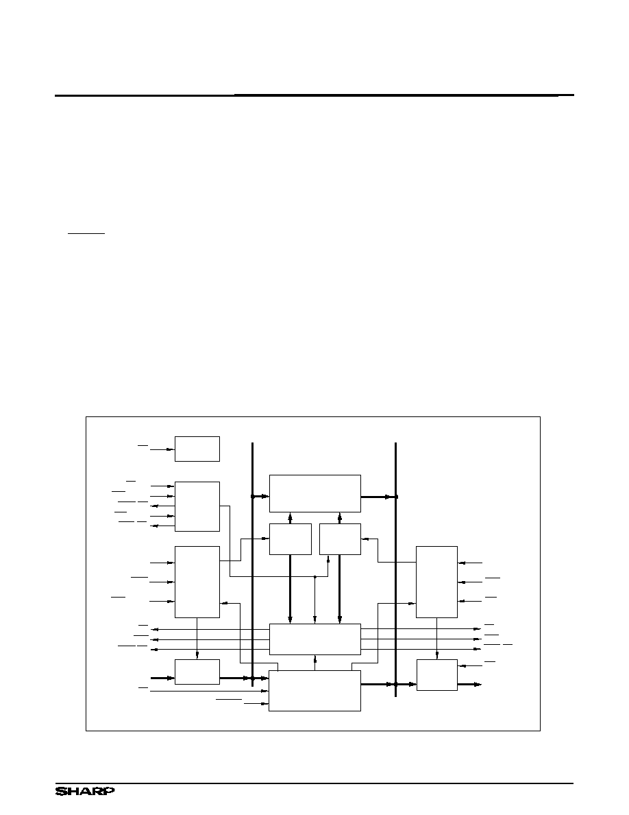
RESET
LOGIC
INPUT
PORT
RS
INPUT
PORT
CONTROL
LOGIC
READ
POINTER
WRITE
POINTER
DEDICATED AND
PROGRAMMABLE
STATUS FLAGS
FIFO
MEMORY ARRAY
2048 x 18/4096 x 18
OUTPUT
PORT
CONTROL
LOGIC
FF
PAF
WXO/HF
RXO
/EF
2
PAE
D
0
- D
17
WEN
WCK
Q
0
- Q
17
RCK
OUTPUT
PORT
REN
OE
PROGRAMMABLE
REGISTERS
EXPANSION
LOGIC
WXI/
WEN
2
FL/
RT
WXO/HF
RXI/
REN
2
RXO/
EF
2
LD
540235-1
WXI/
WEN
2
RXI/
REN
2
BOLD ITALIC = Enhanced Operating Mode.
EMODE
EF
Figure 1. LH540235/45 Block Diagram
BOLD ITALIC = Enhanced Operating Mode
1

FUNCTIONAL DESCRIPTION
NOTE: Throughout this data sheet, a
BOLD ITALIC
type
font is used for all references to
Enhanced Operating
Mode
features which do not function in IDT-Compatible
Operating Mode; and also for all references to the
re-
transmit
facility (which is not an IDT72235B/45B FIFO
feature), even though it may be used ≠ subject to some
restrictions ≠ in either of these two operating modes.
Thus, readers interested only in using the LH540235/45
FIFOs in IDT-Compatible Operating Mode may skip over
BOLD ITALIC
sections, if they wish.
The LH540235/45 parts are FIFO (First-In, First-Out)
memory devices, based on fully-static CMOS dual-port
SRAM technology, capable of containing up to 2048 or 4096
18-bit words respectively. They can replace two or more
byte-wide FIFOs in many applications, for microprocessor-
to-microprocessor or microprocessor-to-bus communica-
tion. Their architecture supports synchronous operation, tied
to two independent free-running clocks at the input and
output ports respectively. However, these `clocks' also may
be aperiodic, asynchronous `demand' signals. Almost all
control-input signals and status-output signals are synchro-
nized to these clocks, to simplify system design.
The input and output ports operate altogether inde-
pendently of each other, unless the FIFO becomes either
totally full or else totally empty. Data flow is initiated at a
port by the rising edge of its corresponding clock, and is
gated by the appropriate edge-sampled enable signals.
The following FIFO status flags monitor the extent to
which the internal memory has been filled: Full, Almost-
Full, Half-Full, Almost-Empty, and Empty. The Almost-Full
and Almost-Empty flag offsets are programmable over the
entire FIFO depth; but, during a reset operation, each of
these is initialized to a default offset value of 12710
FIFO-memory words, from the respective FIFO boundary.
If this default offset value is satisfactory, no further pro-
gramming is required.
After a reset operation during which the
EMODE
control
input was not asserted (was HIGH), these FIFOs operate
in the IDT-Compatible Operating Mode. In this mode,
each part is pin-compatible and functionally-compatible
with the IDT72235B/45B part of similar depth and speed
grade; and the
Control Register
is not even accessible
or visible to the external-system logic which is controlling
the FIFO, although it still performs the same control
functions.
However, assertion of the EMODE control input
during a reset operation leaves Control Register bits
00-05 set, and causes the FIFO to operate in the
Enhanced Operating Mode. In essence, asserting
EMODE chooses a different default state for the Con-
trol Register. The system optionally then may pro-
gram the Control Register in any desired manner to
activate or deactivate any or all of the Enhanced-Op-
erating-Mode features which it can control, including
selectable-clock-edge flag synchronization, and read
inhibition when the data outputs are disabled.
Whenever EMODE is being asserted, interlocked-
operation paralleling also is available, by appropriate
interconnection of the FIFO's expansion inputs.
The retransmit facility is available during standalone
operation, in either IDT-Compatible Operating Mode or
Enhanced Operating Mode (see Tables 1 and 2). It is
inoperative if the FL/
RT
input signal is grounded. It is not
an IDT72235B/45B feature.
The Retransmit control
signal causes the internal FIFO read-address pointer
to be set back to zero, without affecting the internal
FIFO write-address pointer. Thus, the Retransmit
control signal also provides a mechanism whereby a
block of data delimited by the zero physical address
and the current write-address-pointer address may
be read out repeatedly, an arbitrary number of times.
The only restrictions are that neither the read-ad-
dress pointer nor the write-address pointer may
`wrap around' during this entire process, and that the
retransmit facility is not available during depth-cas-
caded operation, either in IDT-Compatible Operating
Mode or in Enhanced Operating Mode (see Tables 1
and 2). Also, the flags behave differently for a short
time after a retransmit operation. Otherwise, the re-
transmit facility is available during standalone opera-
tion, in either IDT-Compatible Operating Mode or
Enhanced Operating Mode.
Note that, when FL/RT is being used as RT, RT is
an assertive-HIGH signal, rather than assertive-LOW
as it is in most other FIFOs having a retransmit
facility.
Programming the programmable-flag offsets,
the tim-
ing synchronization of the various status flags, the
optional read-suppression functionality of OE, and
the behavior of the pointers which access the offset-
value registers and the Control Register
may be indi-
vidually controlled by asserting the signal LD, without any
reset operation. When LD is being asserted, and writing
is being enabled by asserting WEN, some portion of the
input bus word D
0
≠ D
17
is used at the next rising edge of
WCLK to program one or more of the programmable
registers on successive write clocks. Likewise, the values
programmed into these programmable registers may be
read out for verification by asserting LD and REN, with
the outputs Q
0
≠ Q
17
enabled. Reading out these pro-
grammable registers should not be initiated while they are
being written into. Table 3 defines the possible modes of
operation for loading and reading out the contents of
programmable registers.
BOLD ITALIC = Enhanced Operating Mode
LH540235/45
2048 x 18/4096 x 18 Synchronous FIFOs
2
In the Enhanced Operating Mode, coordinated op-
eration of two 18-bit FIFOs as one 36-bit FIFO may be
ensured by `interlocked' crosscoupling of the status-
flag outputs from each FIFO to the expansion inputs
of the other one; that is, FF to WXI/WEN
2
, and EF to
RXI/REN
2
, in both directions between two paralleled
FIFOs. This `interlocked' operation takes effect
automatically, if two paralleled FIFOs are crosscon-
nected in this manner, with the EMODE control input
being asserted (LOW) (see Tables 1 and 2, also Fig-
ures 28 and 31). IDT-compatible depth cascading no
longer is available when operating in this `inter-
locked-paralleled' mode; however, pipelined depth
cascading remains available.
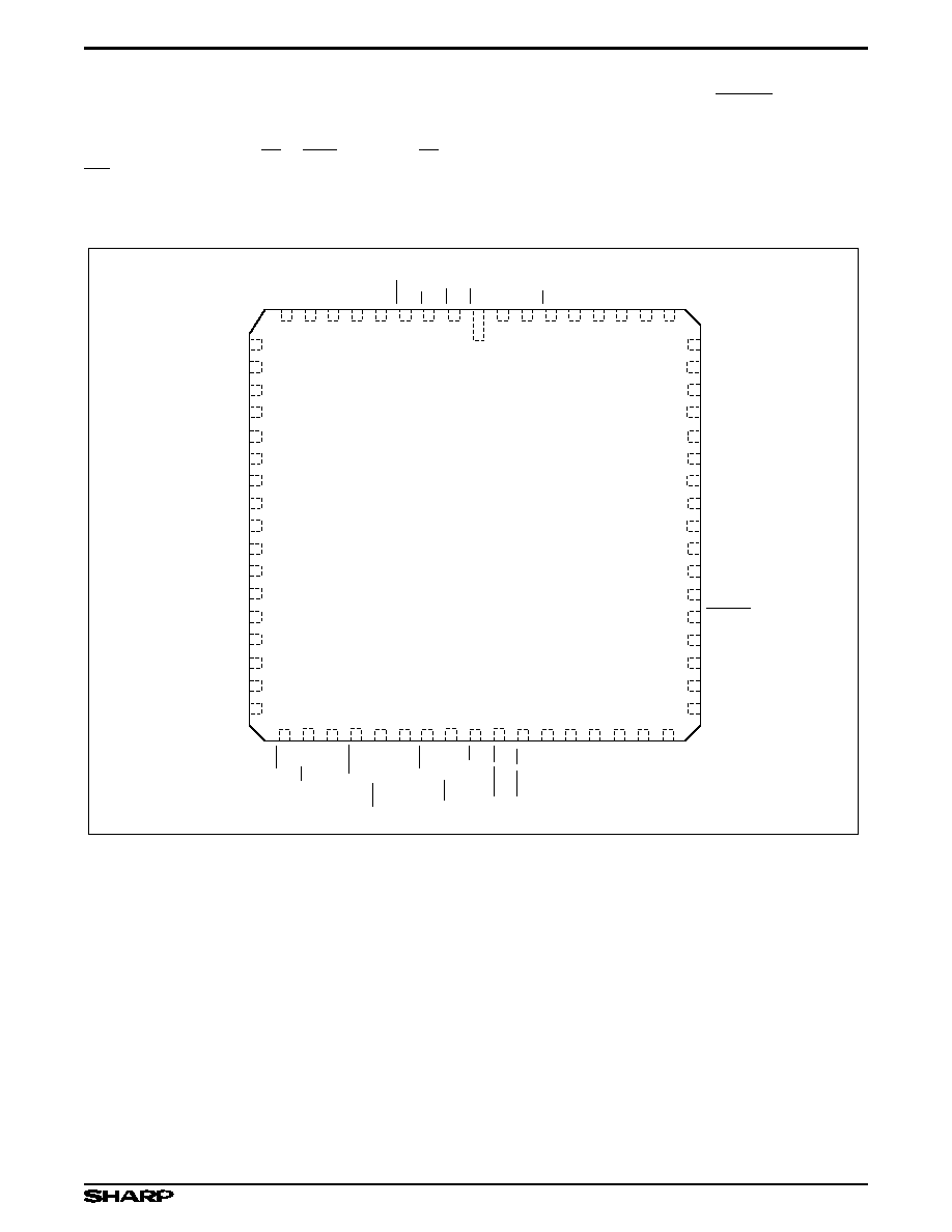
TOP VIEW
540235-2
3
2
1
68 67 66 65 64 63
62 61
9
8
7
6
5
4
Q
17
Q
16
Q
15
LD
OE
V
CC
EF
V
CC
D
15
D
16
D
17
RCLK
REN
RS
16
17
18
19
20
23
24
21
22
26
15
11
12
13
14
10
25
D
2
D
0
D
13
D
14
D
11
D
12
D
9
D
10
D
8
V
CC
D
7
D
5
D
6
D
3
D
4
D
1
55
54
53
52
51
48
47
50
49
46
44
60
59
58
57
56
45
Q
11
V
CC
Q
10
Q
9
Q
8
Q
7
EMODE
Q
6
Q
5
Q
4
V
CC
Q
14
Q
13
Q
12
33 34
35 36 37 38 39 40 41
42 43
27 28 29 30 31 32
Q
2
Q
3
WXO/HF
Q
0
Q
1
V
CC
V
CC
FL/
RT
WCLK
RXO/
EF
2
FF
RXI/
REN
2
PAF
WXI/
WEN
2
WEN
PAE
V
SS
V
SS
V
SS
V
SS
V
SS
V
SS
V
SS
V
SS
BOLD ITALIC = Enhanced Operating Mode.
Figure 2. Pin Connections for PLCC Package
BOLD ITALIC = Enhanced Operating Mode
2048 x 18/4096 x 18 Synchronous FIFOs
LH540235/45
3