 | –≠–ª–µ–∫—Ç—Ä–æ–Ω–Ω—ã–π –∫–æ–º–ø–æ–Ω–µ–Ω—Ç: LH5P832 | –°–∫–∞—á–∞—Ç—å:  PDF PDF  ZIP ZIP |
LH5P832
CMOS 256K (32K
◊
8) Pseudo-Static RAM
FEATURES
∑∑
32,768
◊
8 bit organization
∑∑
Access time: 100/120 ns (MAX.)
∑∑
Cycle time: 160/190 ns (MIN.)
∑∑
Power consumption:
Operating: 357.5/303 mW
Standby: 16.5 mW
∑∑
TTL compatible I/O
∑∑
256 refresh cycle/4 ms
∑∑
Auto refresh is executed by internal
counter (controlled by OE/RFSH pin)
∑∑
Self refresh is executed by internal timer
∑∑
Single +5 V power supply
∑∑
Packages:
28-pin, 600-mil DIP
28-pin, 300-mil SK-DIP
28-pin, 450-mil SOP
DESCRIPTION
The LH5P832 is a 256K bit Pseudo-Static RAM or-
ganized as 32,768
◊
8 bits. It is fabricated using sili-
con-gate CMOS process technology.
The LH5P832 uses convenient on-chip refresh cir-
cuitry with a DRAM memory cell for pseudo static
operation. This simplifies external clock inputs, while
providing the same simple, non-multiplexed pinout as
industry standard SRAMs. Moreover, due to the func-
tional similarities between PSRAMs and SRAMs, many
32K
◊
8 SRAM sockets can be filled with the LH5P832
with little or no changes. The advantage is the cost
savings realized with the lower cost PSRAM.
The LH5P832 PSRAM has the ability to fill the gap
between DRAM and SRAM by offering low cost, low
standby power, and a simple interface.
Three methods of refresh control are provided for
maximum versatility. A `CE-Only' refresh cycle re-
freshes the addressed row of memory cells transpar-
ently. All 256 rows must be refreshed or accessed every
four milliseconds. `Auto Refresh' automatically cycles
through a different row on every OE/RFSH clock pulse,
accomplishing the row refreshes without the need to
supply row addresses externally. `Self Refresh' further
simplifies the refresh requirements by eliminating the
need for address inputs and clock pulses entirely. An
automatic timer senses time periods when memory
accesses have ceased, and provides full refresh of all
rows of memory without any external assistance.
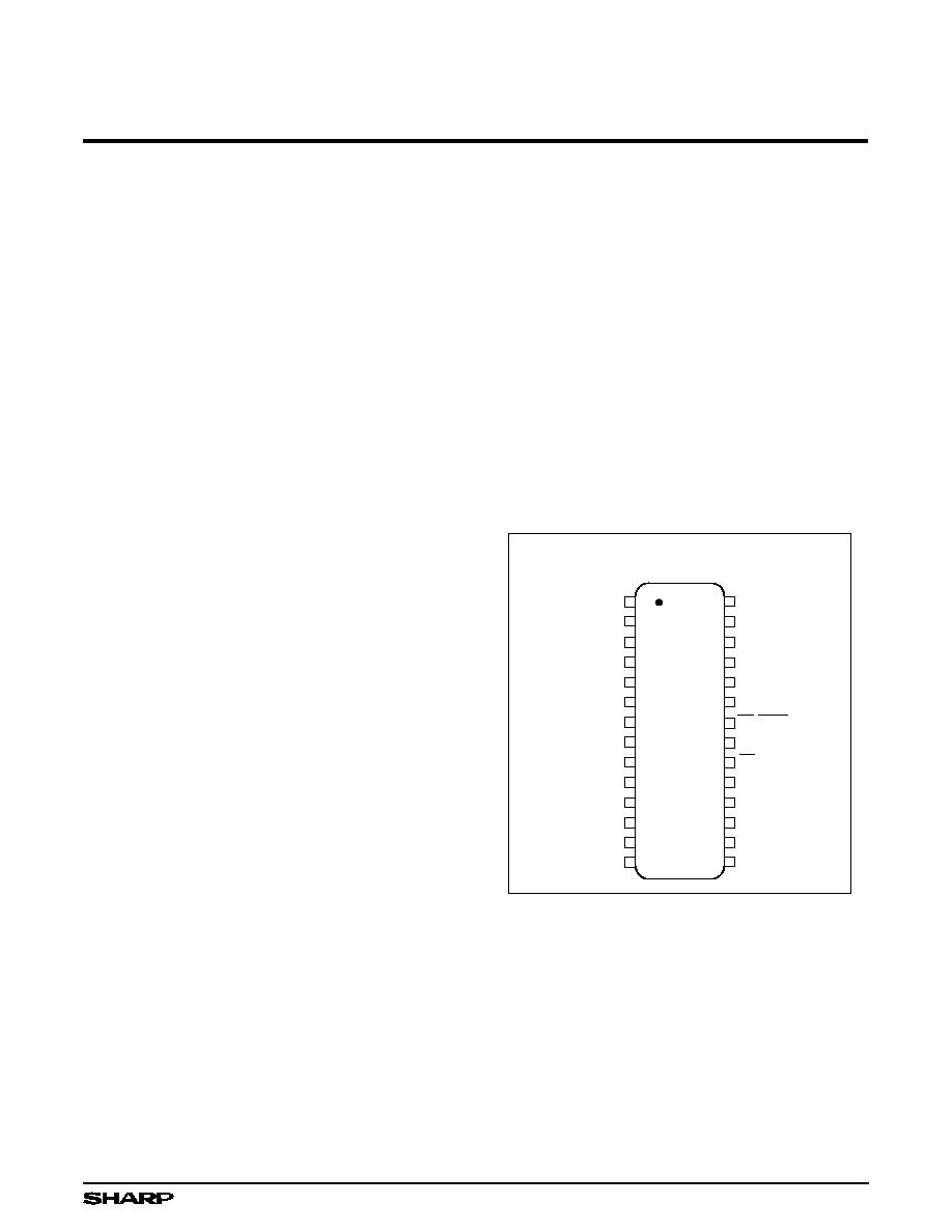
PIN CONNECTIONS
TOP VIEW
1
2
3
4
7
8
A
2
A
5
26
25
24
23
22
21
18
15
A
7
A
6
5
6
A
3
A
4
20
19
A
12
GND
A
8
A
11
A
10
CE
9
10
11
28
27
R/W
A
1
V
CC
12
17
16
A
0
I/O
1
A
9
13
14
OE/RFSH
I/O
2
I/O
3
I/O
7
I/O
6
I/O
5
I/O
4
I/O
8
5P832-1
A
14
A
13
28-PIN DIP
28-PIN SK-DIP
28-PIN SOP
Figure 1. Pin Connections for DIP, SK-DIP,
and SOP Packages
1
5P832-2
I/O
1
20
CLOCK
GENERATOR
27
22
CE
R/W
A
3
A
2
A
1
A
12
A
11
A
10
A
9
A
8
A
7
A
6
A
4
A
5
A
13
A
14
COLUMN
ADDRESS
BUFFER
ROW
ADDRESS
BUFFER
REFRESH
ADDRESS
COUNTER
DATA
IN
BUFFER
DATA
OUT
BUFFER
I/O
SELECTOR
COLUMN
DECODER
SENSE
AMPS
MEMORY
ARRAY
256 ROWS
128 COLUMNS
ROW
DECODER
EXT/INT
ADDRESS
MUX
I/O
2
I/O
3
I/O
4
I/O
5
I/O
6
I/O
7
I/O
8
V
BB
BIAS-GENERATOR
GND
V
CC
OE/
RFSH
16
17
18
19
15
13
12
11
2
23
21
24
26
1
4
7
8
3
6
25
5
9
28
14
A
0
10
SELF-REFRESH
TIMER
AUTO-REFRESH
CONTROLLER
Figure 2. LH5P832 Block Diagram
PIN DESCRIPTION
SIGNAL
PIN NAME
R/W
Read/Write input
OE/RFSH
Output Enable/Refresh input
I/O
1
- I/O
8
Data inputs and outputs
A
0
- A
7
Row address inputs
SIGNAL
PIN NAME
A
8
- A
14
Column Address inputs
CE
Chip Enable input
V
CC
Power supply
GND
Ground
TRUTH TABLE
CE
R/W
OE/RFSH
MODE
I/O
1
- I/O
8
I
CC
NOTE
L
L
X
Write
Data in
Operating (I
CC1
)
1
L
H
L
Read
Data out
Operating (I
CC1
)
L
H
H
CE-Only Refresh
High-Z
Operating (I
CC1
)
H
X
L
Auto Refresh
High-Z
Operating (I
CC1
)
1, 2
H
X
L
Self Refresh
High-Z
Self Refresh (I
CC3
)
1, 3
H
X
H
Standby
High-Z
Standby (I
CC2
)
1
NOTES:
1.
X = H or L 2. OE Pulsewidth < 8
µ
s 3. OE Pulsewidth
8
µ
s
LH5P832
CMOS 256K (32K
◊
8) Pseudo-Static RAM
2
ABSOLUTE MAXIMUM RATINGS
PARAMETER
SYMBOL
RATING
UNIT
NOTE
Applied voltage on any pin
V
T
-1.0 to +7.0
V
1
Output short circuit current
I
O
50
mA
Power dissipation
P
D
600
mW
Operating temperature
Topr
0 to +70
∞
C
Storage temperature
Tstg
-55 to +150
∞
C
NOTE:
1.
Referenced to GND
RECOMMENDED OPERATING CONDITIONS (T
A
= 0 to +70
∞
C)
PARAMETER
SYMBOL
MIN.
TYP.
MAX.
UNIT
Supply voltage
V
CC
4.5
5.0
5.5
V
Input voltage
V
IH
2.4
V
CC
+ 0.3
V
V
IL
-1.0
+0.8
V
CAPACITANCE (V
CC
= 5.0 V
±
10%, T
A
= 0 to +70
∞
C, f = 1 MHz)
PARAMETER
CONDITIONS
SYMBOL
MIN.
MAX.
UNIT
Input capacitance
A
0
- A
14
, R/W
C
IN1
8
pF
CE, OE/RFSH
C
IN2
5
pF
Input/output capacitance
I/O
1
- I/O
8
C
OUT1
12
pF
DC CHARACTERISTICS (V
CC
= 5 V
±
10%, T
A
= 0 to +70
∞
C)
PARAMETER
SYMBOL
CONDITIONS
MIN.
MAX.
UNIT
NOTE
Operating current
I
CC1
tRC = 160 ns
65
mA
1, 2
Operating current
I
CC1
tRC = 190 ns
55
mA
1, 2
Standby current
I
CC2
CE = V
IH
, OE/RFSH = V
IH
3
mA
1
Self refresh average current
I
CC3
CE = V
IH
, OE/RFSH = V
IL
3
mA
1
CPU internal cycle
average current
I
CC4
tRC = 160 ns
65
mA
1, 2
CPU internal cycle
average current
I
CC4
tRC = 190 ns
55
mA
1, 2
Input leakage current
I
LI
0 V
V
IN
6.5 V
-10
10
µ
A
Output leakage current
I
LO
0 V
V
OUT
V
CC
+ 0.3 V
-10
10
µ
A
3
Output High voltage
V
OH
I
OUT
= -1 mA
2.4
V
Output Low voltage
V
OL
I
OUT
= 4 mA
0.4
V
NOTES:
1.
Specified values are with outputs open.
2.
I
CC1
and I
CC4
depend on the cycle time.
3.
The output pins are in high-impedance state.
AC TEST CONDITIONS
PARAMETER
MODE
NOTE
Input voltage amplitude
0.6 to 2.4 V
Input rise/fall time
5 ns
Timing reference level
1.5 V
Output load conditions
1TTL gate, C
L
= 100 pF
1
NOTE:
1.
Includes scope and jig capacitance.
CMOS 256K (32K
◊
8) Pseudo-Static RAM
LH5P832
3
AC CHARACTERISTICS
READ AND WRITE CYCLES
1,2
(V
CC
= 5.0 V
±
10%, T
A
= 0 to 70
∞
C)
PARAMETER
SYMBOL
160 ns
190 ns
UNIT
NOTE
MIN.
MAX.
MIN.
MAX.
Random read, write cycle time
t
RC
160
190
ns
Read modify write cycle time
t
RMW
225
280
ns
CE pulse width
t
CE
100
10,000
120
10,000
ns
CE precharge time
t
P
50
60
ns
Address setup time
t
AS
0
0
ns
Address hold time
t
AH
20
30
ns
Read command hold time
t
RCH
0
0
ns
Read command setup time
t
RCS
0
0
ns
CE access time
t
CEA
100
120
ns
3
OE access time
t
OEA
40
50
ns
3
CE to output in Low-Z
t
CLZ
10
10
ns
OE to output in Low-Z
t
OLZ
0
0
ns
Output enable from end of write
t
WLZ
0
0
ns
Chip disable to output in High-Z
t
CHZ
0
30
0
35
ns
2
Output disable to output in High-Z
t
OHZ
0
30
0
35
ns
2
Write enable to output in High-Z
t
WHZ
0
30
0
35
ns
2
OE setup time
t
OES
10
10
ns
OE hold time
t
OEH
0
0
ns
OE lead time
t
OEL
10
10
ns
Write command pulse width
t
WCP
60
85
ns
Write command setup time
t
WCS
60
85
ns
Write command hold time
t
WCH
60
85
ns
Data setup time from write
t
DSW
40
50
ns
Data setup time from CE
t
DSC
40
50
ns
Data hold time from write
t
DHW
0
0
ns
Data hold time from CE
t
DHC
0
0
ns
Transition time (rise and fall)
t
T
3
35
3
35
ns
Refresh time interval
t
REF
4
4
ms
REFRESH CYCLE
Auto refresh cycle time
t
FC
160
190
ns
Refresh delay time from CE
t
RFD
50
60
ns
Refresh pulse width (Auto refresh)
t
FAP
60
8,000
80
8,000
ns
Refresh precharge time
(Auto refresh)
t
FP
30
30
ns
CE delay time from refresh active
(Auto refresh)
t
FCE
190
225
ns
Refresh pulse width (Self refresh)
t
FAS
8,000
8,000
ns
CE delay time from refresh
precharge (Self refresh)
t
FRS
190
225
ns
NOTES:
1.
At least 200
µ
s of pause time after power on should be given for
proper device operation.
CE and OE/RFSH must be fixed at V
IH
for 200
µ
s from the V
DD
reached to the specified voltage level
and followed by at least 8 dummy cycles.
2.
AC characteristics are measured at t
T
= 5 ns.
3.
Measured with a load circuit equivalent to 1TTL loads and
100 pF.
LH5P832
CMOS 256K (32K
◊
8) Pseudo-Static RAM
4
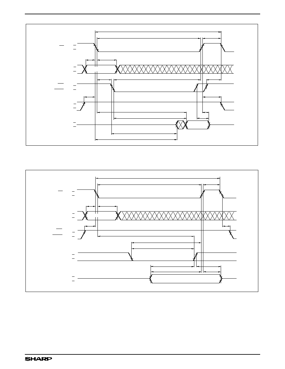
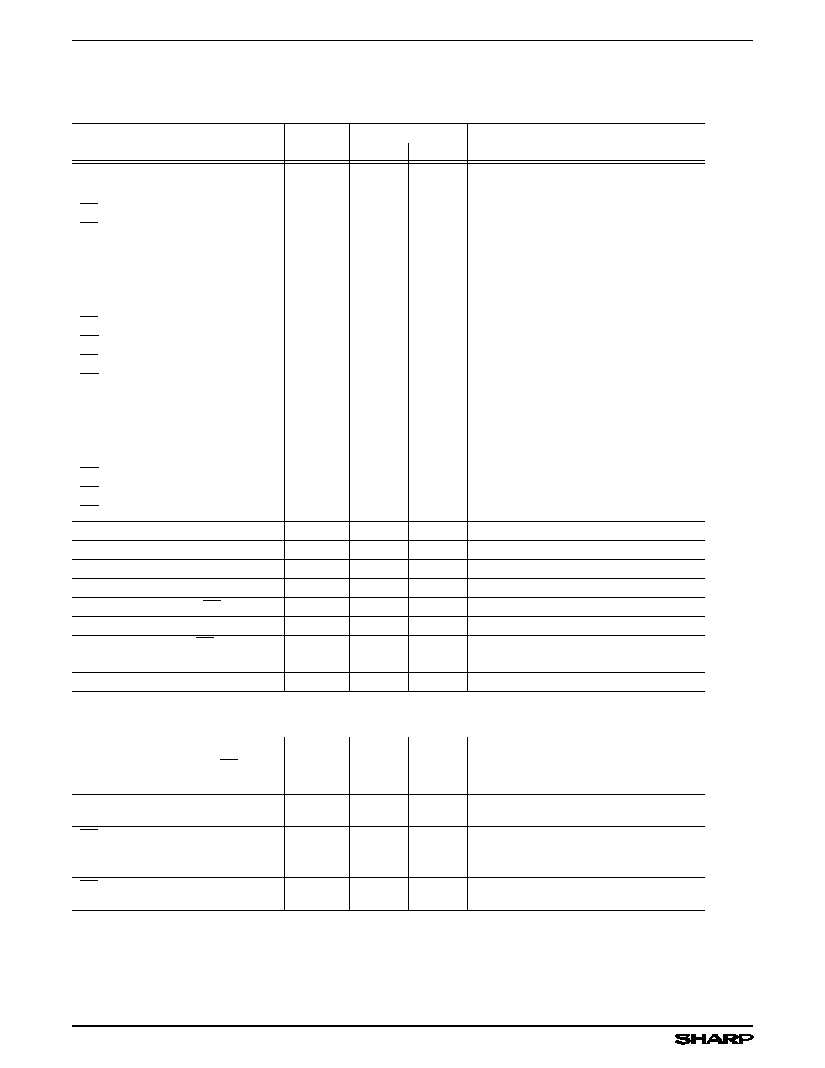
t
CE
ADDRESS
DATA
OUT
t
AS
t
AH
t
OEL
t
OES
t
OEH
t
RCS
t
CHZ
t
OEA
5P832-3
t
P
t
RC
t
RCH
t
CEA
t
OHZ
t
OLZ
t
CLZ
CE
A
0
- A
14
I/O
1
- I/O
8
OE/
RFSH
R/W
V
IH
V
IL
V
IH
V
IL
V
IH
V
IL
V
IH
V
IL
V
OH
V
OL
Figure 3. Read Cycle
t
CE
ADDRESS
t
AS
t
AH
t
WCH
t
OEH
t
OES
t
WCP
5P832-4
t
P
t
RC
t
WCS
CE
A
0
- A
14
I/O
1
- I/O
8
OE/
RFSH
R/W
V
IH
V
IL
V
IH
V
IL
V
IH
V
IL
V
IH
V
IL
DATA - IN
t
DSW
t
DSC
t
DHW
t
DHC
V
IH
V
IL
Figure 4. Write Cycle
CMOS 256K (32K
◊
8) Pseudo-Static RAM
LH5P832
5