 | –≠–ª–µ–∫—Ç—Ä–æ–Ω–Ω—ã–π –∫–æ–º–ø–æ–Ω–µ–Ω—Ç: LH79520 | –°–∫–∞—á–∞—Ç—å:  PDF PDF  ZIP ZIP |

Preliminary Data Sheet
9/10/03
1
LH79520
Preliminary Data Sheet
System-on-Chip
FEATURES
∑ Highly Integrated System-on-Chip
∑ High Performance (77.4144 MHz CPU Speed)
∑ ARM720TTM RISC Core
≠ 32-bit ARM7TDMITM RISC Core
≠ 8KB Cache
≠ MMU (Windows CETM Enabled)
≠ Write Buffer
∑ 32KB On-Chip SRAM
∑ Flexible, Programmable Memory Interface
≠ SDRAM Interface
≠ 15-bit External Address Bus
≠ 32-bit External Data Bus
≠ Two Segments (128MB each)
≠ SRAM/Flash/ROM Interface
≠ 26-bit External Address Bus
≠ 32-bit External Data Bus
≠ Seven Segments (64MB Each)
∑ Multi-stream DMA Controller
≠ Four 32-bit Burst-based Data Streams
∑ Clock and Power Management
≠ 32.768 kHz Oscillator for Real Time Clock
≠ 14.7456 MHz Oscillator and On-chip PLL for
CPU and Bus Clocks
≠ Active, Standby, Sleep and Stop Power Modes
≠ Externally-supplied Clock Options
∑ Low Power Modes
≠ Active Mode: 55 mA (MAX.)
≠ Standby Mode: 35 mA (MAX.)
≠ Sleep Mode: 5.5 mA (MAX.)
≠ Stop Mode 2: 18
µ
A
∑ Watchdog Timer
∑ Vectored Interrupt Controller
≠ 16 Standard and 16 Vectored IRQ Interrupts
≠ Hardware Interrupt Priority
≠ Software Interrupts
≠ FIQ Fast Interrupts
∑ Three UARTs
≠ 16-byte FIFOs for Rx and Tx
≠ IrDA SIR Support
≠ Supports Data Rates Up to 460.8 kb/s
∑ Two 16-bit Pulse Width Modulators
∑ Two Dual Channel Timer Modules
∑ Real Time Clock
≠ 32-bit Up-counter with Programmable Load
≠ Programmable 32-bit Match Compare Register
∑ 64 Programmable General Purpose I/O Signals
≠ Multiplexed with Peripheral I/O Signals
∑ Programmable Color LCD Controller
≠ Up to 800 ◊ 600 Resolution
≠ Supports STN, Color STN, AD-TFT, TFT
≠ Supports 15 Shades of Gray
≠ TFT: Supports 64 k Direct Colors or 256 Colors
selected from a Palette of 64,000 Colors
≠ Color STN: Supports 3,375 Direct Colors or 256
Colors Selected from a Palette of 3,375 Colors
∑ Synchronous Serial Port
≠ Supports Data Rates Up to 1.8452 Mb/s
≠ Compatible with Common Interface Schemes
≠ Motorola SPITM
≠ National Semiconductor MICROWIRETM
≠ Texas Instruments SSI
∑ JTAG Debug Interface and Boundary Scan
∑ 5 V Tolerant I/O
DESCRIPTION
The LH79520, powered by an ARM720T, is a com-
plete System-on-Chip with a high level of integration to
satisfy a wide range of requirements and expectations.
The LH79520 combines a 32-bit ARM720T RISC,
Color LCD controller, Cache, Local SRAM, a number of
essential peripherals such as Direct Memory Access,
Serial and Parallel Interfaces, Infrared support, Timers,
Real Time Clock, Watchdog Timer, Pulse Width Modu-
lators, and an on-chip Phase Lock Loop. Debug is
made simple by JTAG support.
This high level of integration lowers overall system
costs, reduces development cycle time and acceler-
ates product introduction. The LH79520's fully static
design, power management unit, low voltage operation
(1.8 V Core, 3.3 V I/O), on-chip PLL, fast interrupt
response time, on-chip cache and SRAM, powerful
instruction set, and low power RISC core provide high
performance.
To build an advanced portable device, advanced pro-
cessing capability is required. This capability must come
with increased performance in the display system and
peripherals, and yet demand less power from batteries.
The LH79520 is an integrated solution to fit these needs.
ARM720T and ARM7TDMI are trademarks of
Advanced RISC Machines, LTD.
Motorola SPI is a trademark of Motorola, Inc.
National Semiconductor MICROWIRE is a trademark of
National Semiconductor Corporation.
Windows CE is a trademark of Microsoft Corporation.
LH79520
System-on-Chip
2
9/10/03
Preliminary Data Sheet
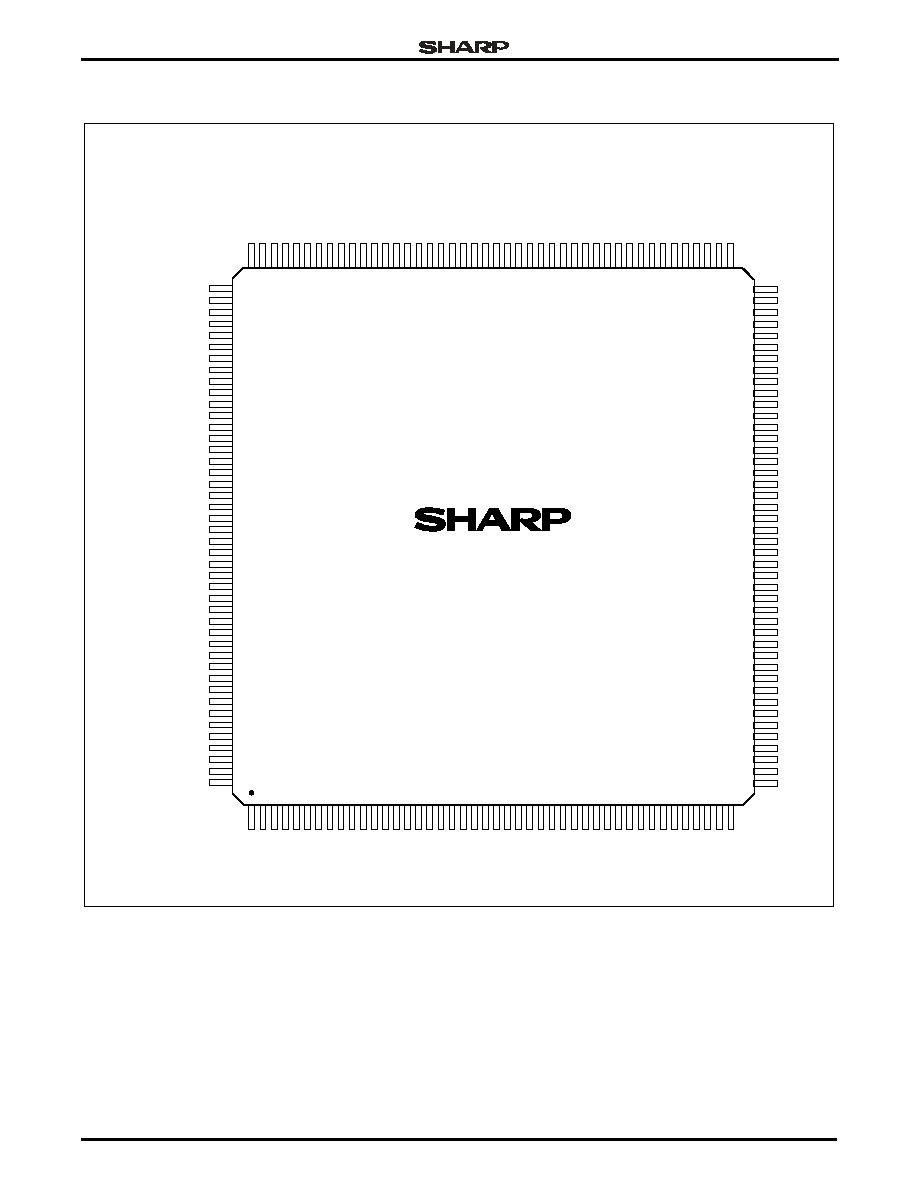
PIN DIAGRAM
Figure 1. 176-Pin LQFP
120
121
122
123
124
125
126
127
128
129
130
131
132
119
118
117
116
115
114
113
112
111
110
109
108
107
106
105
104
103
102
101
100
99
98
97
96
95
94
93
92
91
90
89
1
2
3
4
5
6
7
8
9
10
11
12
13
14
15
16
17
18
19
20
21
22
23
24
25
26
27
28
29
30
31
A25
nTSTA
A22
A21
A19
A18
VSS
A15
A12
VSS
A7
A5
VDD
A2
A0
PH7/nBLE3
32
33
A10
PC6/LCDVD17
PC7/LCDFP/
LCDSPS
VSS
LCDVD0
VDD
PD0/LCDVD2
PD1/LCDVD3
PD3/LCDVD5
VSSC
PD4/LCDVD6/
LCDPS
PD6/LCDVD8
PD7/LCDVD9
INT7/LCDVD11
PE1/DQM1
PE2/DQM2
PE0/DQM0
nCAS
PF0/SDCLK
VDD
PF1/CLKEN
PD2/LCDVD4
PD5/LCDVD7
PE3/DQM3
PE7/SDCKE
VSS
PE6/nDCS1
PE4/nSDWE
nRAS
CLKIN
/
UARTCLK
TOP VIEW
79520-100
34
35
36
37
38
39
40
nBLE0
nOE
nRESETOUT
nRESETIN
VDDC
XTALOUT
XTALIN
VSSA
VDDA
77
76
41
42
43
44
88
87
86
85
84
83
82
81
80
79
78
75
74
73
72
71
70
69
68
67
66
65
64
63
62
61
60
59
56
57
55
54
53
52
51
50
49
48
47
46
45
58
INT5/DREQ1/nWAIT
CTOUT1B/DACK1
PC3/LCDDCLK
PC2/LCDDCLKIN
PC1/LCDVDDEN/LCDCLS
VDDC
PC0/LCDENAB/LCDSPL
VSSC
PB7/LCDVD15/LCDDSPLEN
PB6/LCDVD14
PB5/LCDVD13
PB4/LCDVD12/LCDREV
VDD
PB3/DREQ0
PB2/nDACK0
PB1/DEOT0
VSS
INT4/PWM0
INT3/PWMSYNC0
PB0/INT2
PA7/INT1
VDDC
PA6/INT0
PA5/CLKOUT
PWM1/DEOT1
VSSC
PA4/UARTTX1
PA3/UARTRX1
VDD
UARTIRTX0/UARTTX0
PA1/SSPCLK
PA2/SSPFRM
PA0/SSPEN
SSPTX/UARTTX2
VSS
SSPRX/UARTRX2
TMS
TDO
TDI
TCLK
nTRST
TEST1
TEST2
UARTIRRX0/UARTRX0
D8
D9
CLKINSEL
D0
D1
VDD
D2
D3
D4
D5
VSS
D6
D7
VDDC
D10
D11
D12
D13
VSS
D14
D15
PF2/D16
PF3/D17
PF4/D18
VDD
PF5/D19
PF6/D20
PF7/D21
PG0/D22
PG1/D23
PG4/D26
PG3/D25
VSS
PG5/D27
PG6/D28
PG7/D29
PH0/D30
PH1/D31
VDD
nCS0
nCS1
nCS2
VSSC
PG2/D24
144
145
133
134
135
136
137
138
139
140
141
142
143
146
147
148
149
150
151
152
153
154
155
156
157
158
159
160
161
162
165
164
166
167
168
169
170
171
172
173
174
175
176
163
A23
A20
VDD
A17
A16
A14
A13
VDD
A11
A6
A4
A3
A1
VSS
PH6/nBLE2
nBLE1
PH5/nCS6
PH4/nCS5
nWE
VDDC
LCDVD1
VDDC
INT6/LCDVD10
A8
A9
176-PIN LQFP
PH3/nCS4
PH2/nCS3
XTAL32OUT
XTAL32IN
PC4/LCDVD16
PC5/LCDLP
A24
PE5/nDCS0
LH79520

System-on-Chip
LH79520
Preliminary Data Sheet
9/10/03
3
Figure 2. LH79520 Block Diagram
79520-1B
OSCILLATOR,
PLL POWER
MANAGEMENT, and
RESET CONTROL
VECTORED
INTERRUPT
CONTROLLER
32KB
SRAM
14.7456 MHz
32.768 kHz
REAL TIME
CLOCK
INTERNAL
INTERRUPTS
CONDITIONED
EXTERNAL
INTERRUPTS
SDRAM
CONTROLLER
COLOR
LCD
CONTROLLER
STATIC
MEMORY
CONTROLLER
EXTERNAL
BUS
INTERFACE
TEST
LOGIC / PIN
MUXING
ARM 720T
RESET
EXTERNAL
INTERRUPTS
DEBUG/TEST
INTERFACE
ADVANCED
PERIPHERAL
BUS BRIDGE
DMA
CONTROLLER
ADVANCED HIGH
PERFORMANCE
BUS (AHB)
ADVANCED
PERIPHERAL
BUS (APB)
GENERAL
PURPOSE I/O
I/O
CONFIGURATION
SYNCHRONOUS
SERIAL PORT
TIMER (4)
WATCHDOG
TIMER
DUAL
CHANNEL PWM
UART (3)
IrDA
INTERFACE
ADVANCED
LCD
INTERFACE
LH79520
System-on-Chip
4
9/10/03
Preliminary Data Sheet
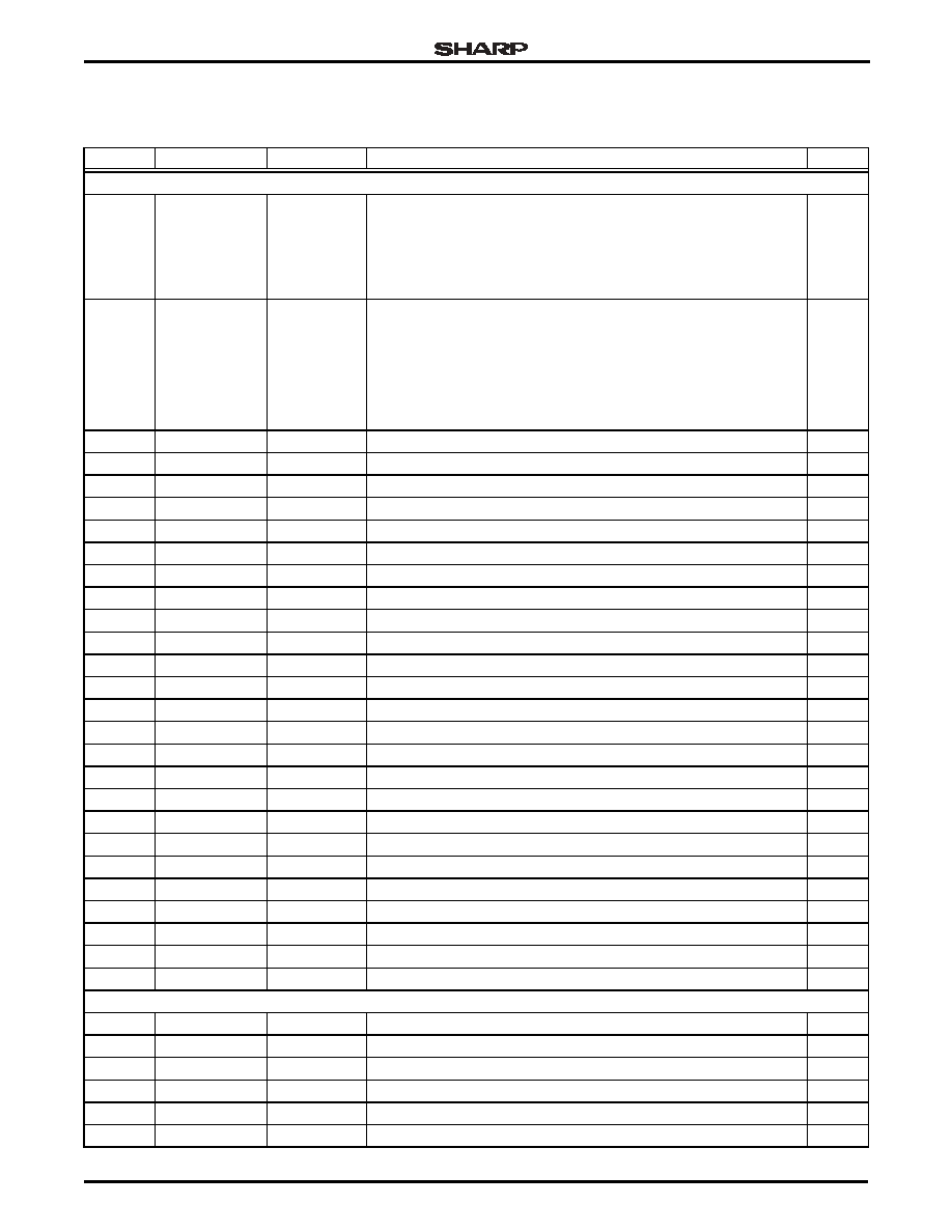
SIGNAL DESCRIPTIONS
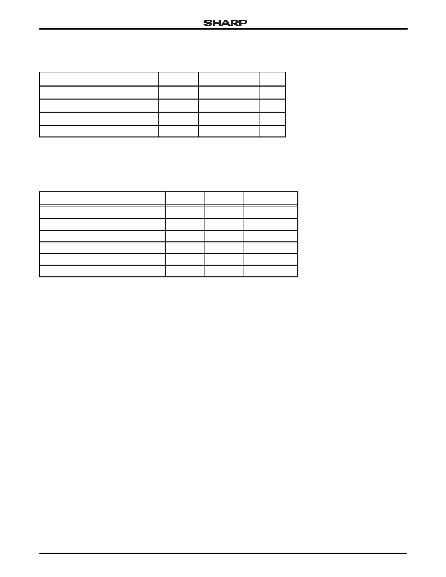
Table 1. LH79520 Signal Descriptions
PIN NO.
SIGNAL NAME
TYPE
DESCRIPTION
NOTES
MEMORY INTERFACE (MI)
2-7
9-12
14-17
19-22
24-27
29-32
A[25:0]
Output
Address Signals
50-54
56-63
65-66
67-69
71-74
76-79
81-84
86-87
D[31:0]
Input/Output
Data Input/Output Signals
1
101
SDCLK
Output
SDRAM Clock
1
109
DQM3
Output
Data Mask Output to SDRAMs
1
110
DQM2
Output
Data Mask Output to SDRAMs
1
111
DQM1
Output
Data Mask Output to SDRAMs
1
112
DQM0
Output
Data Mask Output to SDRAMs
1
102
SDCKE
Output
SDRAM Clock Enable
1
104
nDCS1
Output
SDRAM Chip Select
1
105
nDCS0
Output
SDRAM Chip Select
1
107
nRAS
Output
Row Address Strobe
108
nCAS
Output
Column Address Strobe
106
nSDWE
Output
SDRAM Write Enable
1
41
nCS6
Output
Static Memory Controller Chip Select
1
42
nCS5
Output
Static Memory Controller Chip Select
1
43
nCS4
Output
Static Memory Controller Chip Select
1
44
nCS3
Output
Static Memory Controller Chip Select
1
46
nCS2
Output
Static Memory Controller Chip Select
47
nCS1
Output
Static Memory Controller Chip Select
48
nCS0
Output
Static Memory Controller Chip Select
38
nOE
Output
Static Memory Controller Output Enable
34
nBLE3
Output
Static Memory Controller Byte Lane Enable / Byte Write Enable
1
35
nBLE2
Output
Static Memory Controller Byte Lane Enable / Byte Write Enable
1
36
nBLE1
Output
Static Memory Controller Byte Lane Enable / Byte Write Enable
37
nBLE0
Output
Static Memory Controller Byte Lane Enable / Byte Write Enable
39
nWE
Output
Static Memory Controller Write Enable
144
nWAIT
Input
Static Memory Controller External Wait Control
1, 3
DMA CONTROLLER (DMAC)
148
DEOT0
Output
DMA 0 End of Transfer
1
147
nDACK0
Output
DMA 0 Acknowledge
1
146
DREQ0
Input
DMA 0 Request
1
157
DEOT1
Output
DMA 1 End of Transfer
1
145
DACK1
Output
DMA 1 Acknowledge
1
144
DREQ1
Input
DMA 1 Request
1, 3

System-on-Chip
LH79520
Preliminary Data Sheet
9/10/03
5
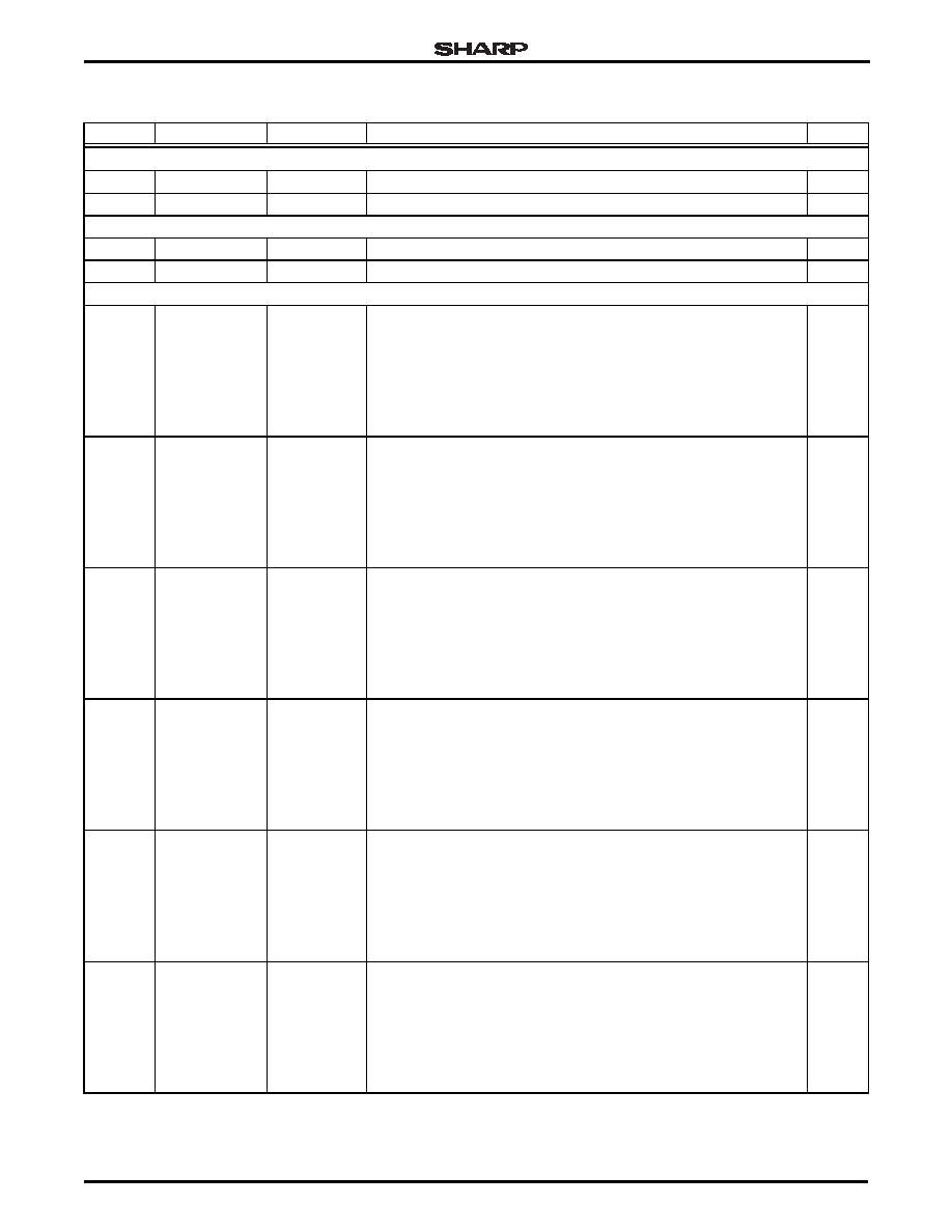
COLOR LCD CONTROLLER (CLCDC)
130
132
139
140
141
142
114
115
116
117
118
119
121
122
123
124
126
127
LCDVD[17:0]
Output
LCD Panel Data bus
1
137
LCDENAB
Output
LCD Data Enable
1
129
LCDFP
Output
Frame Pulse (STN), Vertical Synchronization Pulse (TFT)
1
131
LCDLP
Output
Line Synchronization Pulse (STN),
Horizontal Synchronization Pulse (TFT)
1
133
LCDDCLK
Output
LCD Panel Data Clock
1
139
LCDDSPLEN
Output
LCD Display Enable
1
134
LCDDCLKIN
Input
LCD External Clock Input
1
135
LCDVDDEN
Output
LCD Digital Supply Enable
1
135
LCDCLS
Output
LCD Clock Signal for Gate Driver (HR-TFT only)
1
129
LCDSPS
Output
LCD Reset Signal for Row Display (HR-TFT only)
1
142
LCDREV
Output
LCD Reverse Signal (HR-TFT only)
1
137
LCDSPL
Output
LCD Line Start Pulse (Left) (HR-TFT only)
1
119
LCDPS
Output
LCD Power Save (HR-TFT only)
1
SYNCHRONOUS SERIAL PORT (SSP)
164
SSPFRM
Output
SSP Serial Frame Output
1
165
SSPCLK
Output
SSP Clock
1
166
SSPEN
Output
SSP Data Enable
1
167
SSPTX
Output
SSP Data Out
1
169
SSPRX
Input
SSP Data In
1
PULSE WIDTH MODULATOR (PWM)
150
PWM0
Output
PWM0 Output
1
151
PWMSYNC0
Input
PWM0 Synchronizing Input
1
157
PWM1
Output
PWM1 Output
1
UART0 (U0)
163
UARTRX0
Input
UART0 Received Serial Data Input
1
162
UARTTX0
Output
UART0 Transmitted Serial Data Output
1
163
UARTIRRX0
Input
UART0 InfraRed Receive
1
162
UARTIRTX0
Output
UART0 InfraRed Transmit
1
Table 1. LH79520 Signal Descriptions (Cont'd)
PIN NO.
SIGNAL NAME
TYPE
DESCRIPTION
NOTES
LH79520
System-on-Chip
6
9/10/03
Preliminary Data Sheet
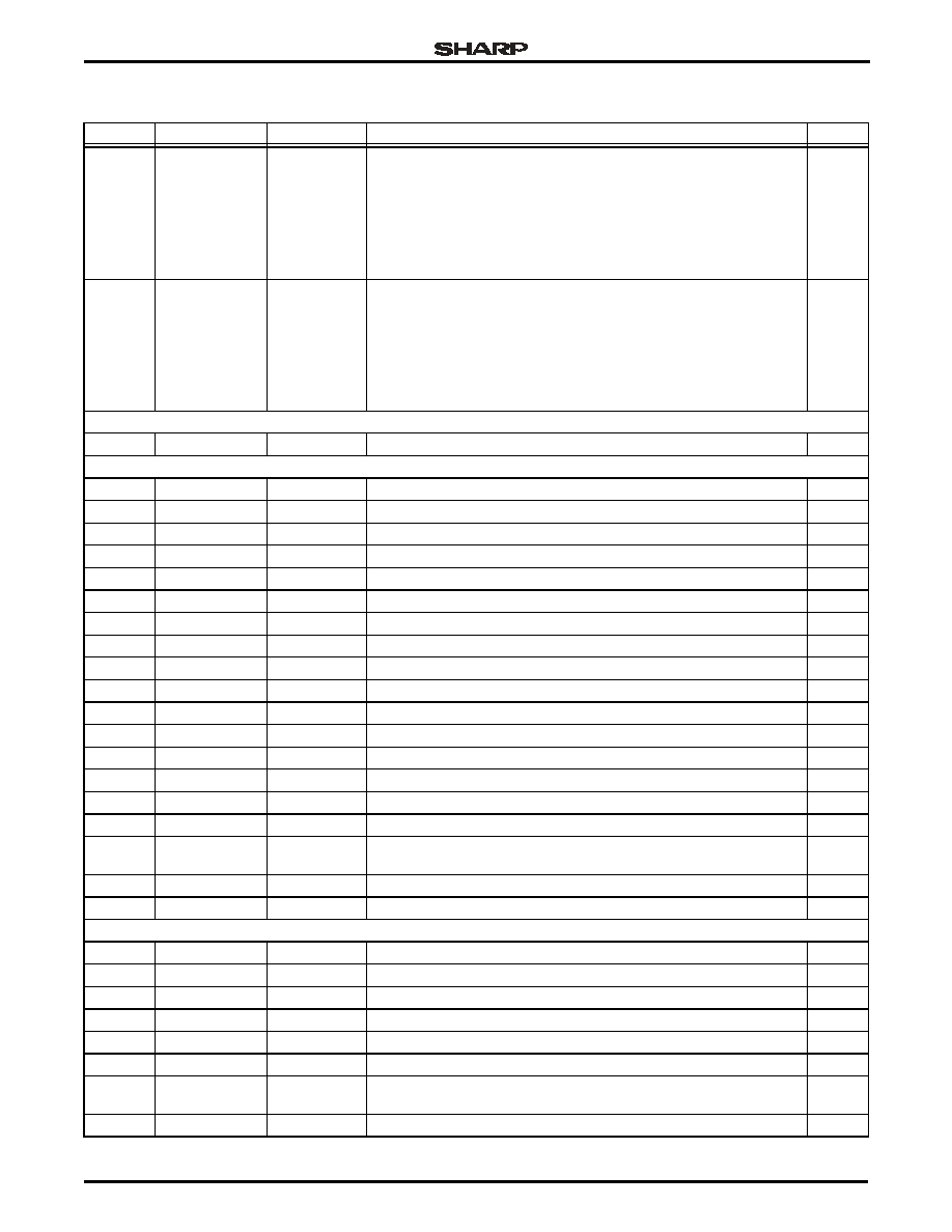
UART1 (U1)
160
UARTRX1
Input
UART1 Received Serial Data Input
1
159
UARTTX1
Output
UART1 Transmitted Serial Data Output
1
UART2 (U2)
169
UARTRX2
Input
UART2 Received Serial Data Input
1
167
UARTTX2
Output
UART2 Transmitted Serial Data Output
1
GENERAL PURPOSE INPUT/OUTPUT (GPIO)
153
155
156
159
160
164
165
166
PA7
PA6
PA5
PA4
PA3
PA2
PA1
PA0
Input/Output
General Purpose I/O Signals - Port A
1
139
140
141
142
146
147
148
152
PB7
PB6
PB5
PB4
PB3
PB2
PB1
PB0
Input/Output
General Purpose I/O Signals - Port B
1
129
130
131
132
133
134
135
137
PC7
PC6
PC5
PC4
PC3
PC2
PC1
PC0
Input/Output
General Purpose I/O Signals - Port C
1
116
117
118
119
121
122
123
124
PD7
PD6
PD5
PD4
PD3
PD2
PD1
PD0
Input/Output
General Purpose I/O Signals - Port D
1
102
104
105
106
109
110
111
112
PE7
PE6
PE5
PE4
PE3
PE2
PE1
PE0
Input/Output
General Purpose I/O Signals - Port E
1
61
62
63
65
66
67
99
101
PF7
PF6
PF5
PF4
PF3
PF2
PF1
PF0
Input/Output
General Purpose I/O Signals - Port F.
GPIO PF1 is only available when CLKINSEL is `0'
(i.e. the external clock source is not being used).
1
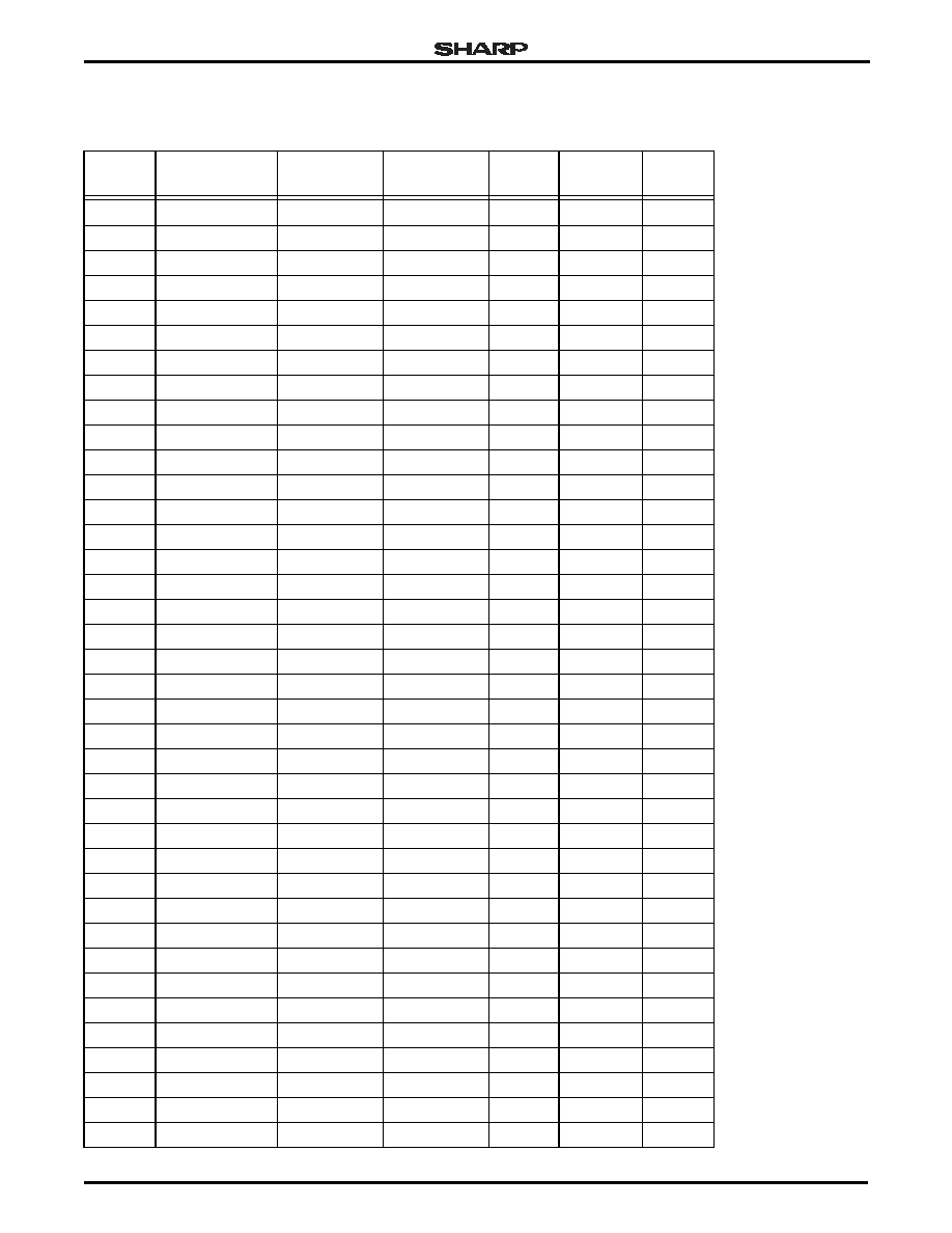
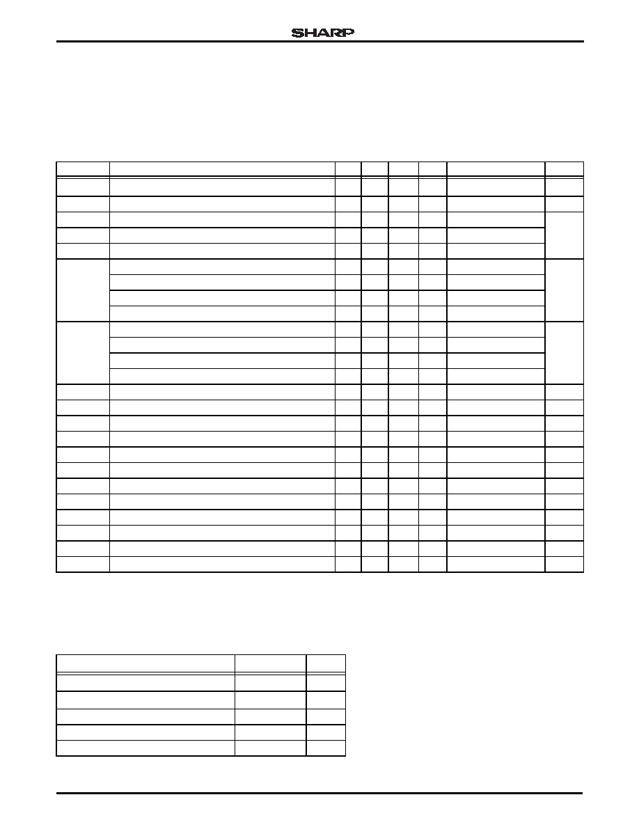
Table 1. LH79520 Signal Descriptions (Cont'd)
PIN NO.
SIGNAL NAME
TYPE
DESCRIPTION
NOTES
System-on-Chip
LH79520
Preliminary Data Sheet
9/10/03
7
52
53
54
56
57
58
59
60
PG7
PG6
PG5
PG4
PG3
PG2
PG1
PG0
Input/Output
General Purpose I/O Signals - Port G
1
34
35
41
42
43
44
50
51
PH7
PH6
PH5
PH4
PH3
PH2
PH1
PH0
Input/Output
General Purpose I/O Signals - Port H
1
COUNTER/TIMER (C/T)
145
CTOUT1B
Output
Counter/Timer Output
1
RESET, CLOCK, AND POWER CONTROLLER (RCPC)
96
nRESETIN
Input
Reset Input
97
nRESETOUT
Output
Reset Output
114
INT7
Input
External Interrupt Input
1
115
INT6
Input
External Interrupt Input
1
144
INT5
Input
External Interrupt Input
1, 3
150
INT4
Input
External Interrupt Input
1
151
INT3
Input
External Interrupt Input
1
152
INT2
Input
External Interrupt Input
1
153
INT1
Input
External Interrupt Input
1
155
INT0
Input
External Interrupt Input
1
93
XTALIN
Input
Crystal Input
94
XTALOUT
Output
Crystal Output
89
XTAL32IN
Input
32.768 kHz Crystal Oscillator Input
90
XTAL32OUT
Output
32.768 kHz Crystal Oscillator Output
88
CLKINSEL
Input
External Clock Select
98
CLKIN
Input
External Clock Input (if CLKINSEL = HIGH at reset)
1
99
CLKEN
Output
External Clock Enable
(if CLKINSEL = LOW at reset, then this pin functions as PF1)
1
156
CLKOUT
Output
Clock Out (selectable from the internal bus clock or 32.768)
1
98
UARTCLK
Input
External UART Clock Input (with CLKSEL = LOW)
1
TEST INTERFACE
174
nTRST
Input
JTAG Test Reset Input
170
TMS
Input
JTAG Test Mode Select Input
173
TCLK
Input
JTAG Test Clock Input
172
TDI
Input
JTAG Test Serial Data Input
171
TDO
Output
JTAG Test Data Serial Output
175
TEST1
Input
Tie LOW for Normal Operation (has internal pull-down).
176
TEST2
Input
JTAG Debug Enable: Tie LOW for Normal Operation; pull HIGH to
enable JTAG Debugging (has internal pull-down).
1
nTSTA
Input
Tie HIGH for Normal Operation (has internal pull-up).
Table 1. LH79520 Signal Descriptions (Cont'd)
PIN NO.
SIGNAL NAME
TYPE
DESCRIPTION
NOTES

LH79520
System-on-Chip
8
9/10/03
Preliminary Data Sheet
1. These pin numbers have multiplexed functions.
2. Signals preceded by `n' are Active LOW.
3. Immediately after reset, pin 144 can be programmed to function as INT5, DREQ1 or both.
Software should avoid enabling both of these functions simultaneously. Pin 144 can also be
programmed to function as nWAIT, rendering the INT5/DREQ1 choice unavailable.
POWER AND GROUND (GND)
40
75
95
113
136
154
VDDC
Power
Core Power Supply
45
120
138
158
VSSC
Ground
Core GND
8
18
28
49
64
85
100
125
143
161
VDD
Power
Input/Output Power Supply
13
23
33
55
70
80
103
128
149
168
VSS
Ground
Input/Output GND
91
VDDA
Power
Analog Power Supply for PLLs and XTAL Oscillators
92
VSSA
Ground
Analog GND for PLLs and XTAL Oscillators
Table 1. LH79520 Signal Descriptions (Cont'd)
PIN NO.
SIGNAL NAME
TYPE
DESCRIPTION
NOTES
System-on-Chip
LH79520
Preliminary Data Sheet
9/10/03
9
NUMERCIAL PIN LIST
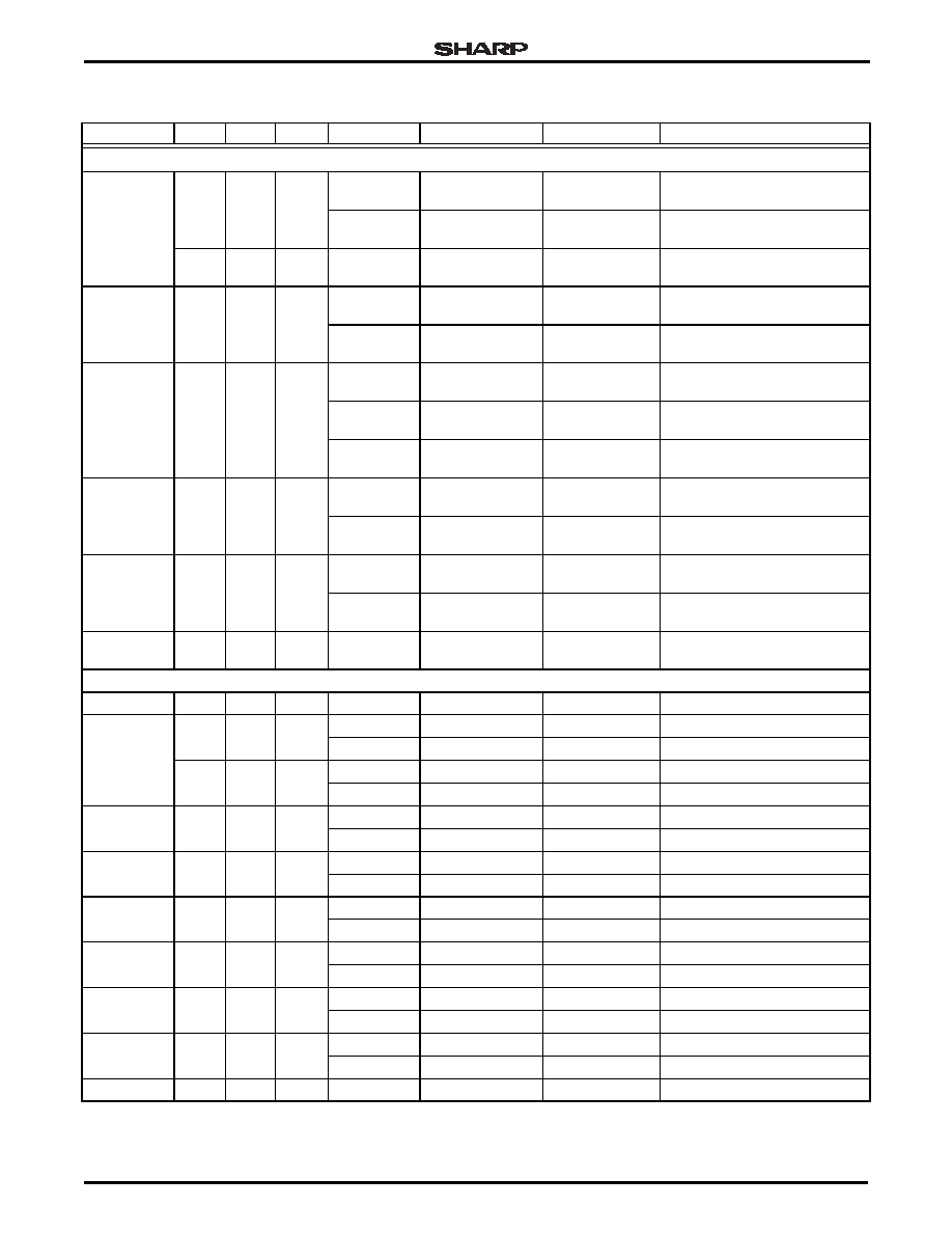
Table 2. LH79520 Numerical Pin List
PIN NO.
FUNCTION AT
RESET
FUNCTION 2 FUNCTION 3
TYPE
5
OUTPUT
DRIVE
7
NOTES
1
nTSTA
Input
None
1
2
A25
Output
8 mA
3
A24
Output
8 mA
4
A23
Output
8 mA
5
A22
Output
8 mA
6
A21
Output
8 mA
7
A20
Output
8 mA
8
VDD
Power
None
9
A19
Output
8 mA
10
A18
Output
8 mA
11
A17
Output
8 mA
12
A16
Output
8 mA
13
VSS
Ground
None
14
A15
Output
8 mA
15
A14
Output
8 mA
16
A13
Output
8 mA
17
A12
Output
8 mA
18
VDD
Power
None
19
A11
Output
8 mA
20
A10
Output
8 mA
21
A9
Output
8 mA
22
A8
Output
8 mA
23
VSS
Ground
None
24
A7
Output
8 mA
25
A6
Output
8 mA
26
A5
Output
8 mA
27
A4
Output
8 mA
28
VDD
Power
None
29
A3
Output
8 mA
30
A2
Output
8 mA
31
A1
Output
8 mA
32
A0
Output
8 mA
33
VSS
Ground
None
34
PH7
nBLE3
I/O
8 mA
35
PH6
nBLE2
I/O
8 mA
36
nBLE1
Output
8 mA
37
nBLE0
Output
8 mA
38
nOE
Output
8 mA
LH79520
System-on-Chip
10
9/10/03
Preliminary Data Sheet
39
nWE
Output
8 mA
40
VDDC
Power
None
41
PH5
nCS6
I/O
8 mA
42
PH4
nCS5
I/O
8 mA
43
PH3
nCS4
I/O
8 mA
44
PH2
nCS3
I/O
8 mA
45
VSSC
Ground
None
46
nCS2
Output
8 mA
47
nCS1
Output
8 mA
48
nCS0
Output
8 mA
49
VDD
Power
None
50
PH1
D31
I/O
8 mA
51
PH0
D30
I/O
8 mA
52
PG7
D29
I/O
8 mA
53
PG6
D28
I/O
8 mA
54
PG5
D27
I/O
8 mA
55
VSS
Ground
None
56
PG4
D26
I/O
8 mA
57
PG3
D25
I/O
8 mA
58
PG2
D24
I/O
8 mA
59
PG1
D23
I/O
8 mA
60
PG0
D22
I/O
8 mA
61
PF7
D21
I/O
8 mA
62
PF6
D20
I/O
8 mA
63
PF5
D19
I/O
8 mA
64
VDD
Power
None
65
PF4
D18
I/O
8 mA
66
PF3
D17
I/O
8 mA
67
PF2
D16
I/O
8 mA
68
D15
I/O
8 mA
69
D14
I/O
8 mA
70
VSS
Ground
None
71
D13
I/O
8 mA
72
D12
I/O
8 mA
73
D11
I/O
8 mA
74
D10
I/O
8 mA
75
VDDC
Power
None
76
D9
I/O
8 mA
77
D8
I/O
8 mA
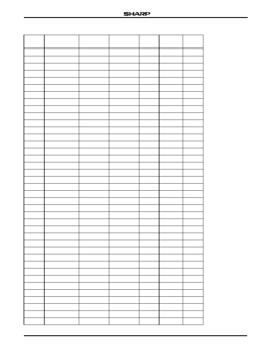
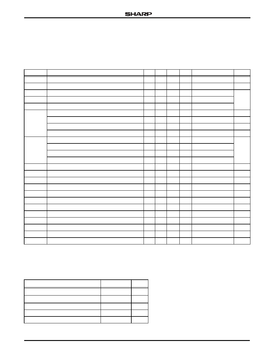
Table 2. LH79520 Numerical Pin List (Cont'd)
PIN NO.
FUNCTION AT
RESET
FUNCTION 2 FUNCTION 3
TYPE
5
OUTPUT
DRIVE
7
NOTES

System-on-Chip
LH79520
Preliminary Data Sheet
9/10/03
11
78
D7
I/O
8 mA
79
D6
I/O
8 mA
80
VSS
Ground
None
81
D5
I/O
8 mA
82
D4
I/O
8 mA
83
D3
I/O
8 mA
84
D2
I/O
8 mA
85
VDD
Power
None
86
D1
I/O
8 mA
87
D0
I/O
8 mA
88
CLKINSEL
Input
None
2
89
XTAL32IN
Input
None
8
90
XTAL32OUT
Output
3
91
VDDA
Power
None
92
VSSA
Ground
None
93
XTALIN
Input
None
8
94
XTALOUT
Output
3
95
VDDC
Power
None
96
nRESETIN
Input
None
1, 4
97
nRESETOUT
Output
4 mA
98
CLKIN
UARTCLK
Input
None
99
PF1
CLKEN
I/O
2 mA
100
VDD
Power
None
101
PF0
SDCLK
I/O
8 mA
102
PE7
SDCKE
I/O
8 mA
103
VSS
Ground
None
104
PE6
nDCS1
I/O
8 mA
105
PE5
nDCS0
I/O
8 mA
106
PE4
nSDWE
I/O
8 mA
107
nRAS
Output
8 mA
108
nCAS
Output
8 mA
109
PE3
DQM3
I/O
8 mA
110
PE2
DQM2
I/O
8 mA
111
PE1
DQM1
I/O
8 mA
112
PE0
DQM0
I/O
8 mA
113
VDDC
Power
None
114
INT7
LCDVD11
I/O
8 mA
4
115
INT6
LCDVD10
I/O
8 mA
4
116
PD7
LCDVD9
I/O
8 mA
Table 2. LH79520 Numerical Pin List (Cont'd)
PIN NO.
FUNCTION AT
RESET
FUNCTION 2 FUNCTION 3
TYPE
5
OUTPUT
DRIVE
7
NOTES

LH79520
System-on-Chip
12
9/10/03
Preliminary Data Sheet
117
PD6
LCDVD8
I/O
8 mA
118
PD5
LCDVD7
I/O
8 mA
119
PD4
LCDVD6
LCDPS
I/O
8 mA
120
VSSC
Ground
None
121
PD3
LCDVD5
I/O
8 mA
122
PD2
LCDVD4
I/O
8 mA
123
PD1
LCDVD3
I/O
8 mA
124
PD0
LCDVD2
I/O
8 mA
125
VDD
Power
None
126
LCDVD1
Output
8 mA
127
LCDVD0
Output
8 mA
128
VSS
Ground
None
129
PC7
LCDFP
LCDSPS
I/O
8 mA
130
PC6
LCDVD17
I/O
8 mA
131
PC5
LCDLP
I/O
8 mA
132
PC4
LCDVD16
I/O
8 mA
133
PC3
LCDDCLK
I/O
8 mA
134
PC2
LCDDCLKIN
I/O
2 mA
135
PC1
LCDVDDEN
LCDCLS
I/O
8 mA
136
VDDC
Power
None
137
PC0
LCDENAB
LCDSPL
I/O
8 mA
138
VSSC
Ground
None
139
PB7
LCDVD15
LCDDSPLEN
I/O
8 mA
140
PB6
LCDVD14
I/O
8 mA
141
PB5
LCDVD13
I/O
8 mA
142
PB4
LCDVD12
LCDREV
I/O
8 mA
143
VDD
Power
None
144
INT5/DREQ1
nWAIT
Input
None
4, 6
145
CTOUT1B
DACK1
Output
4 mA
146
PB3
DREQ0
I/O
2 mA
4
147
PB2
nDACK0
I/O
4 mA
148
PB1
DEOT0
I/O
4 mA
149
VSS
Ground
None
150
INT4
PWM0
I/O
4 mA
4
151
INT3
PWMSYNC0
Input
None
4
152
PB0
INT2
I/O
2 mA
4
153
PA7
INT1
I/O
2 mA
4
154
VDDC
Power
None
155
PA6
INT0
I/O
2 mA
4
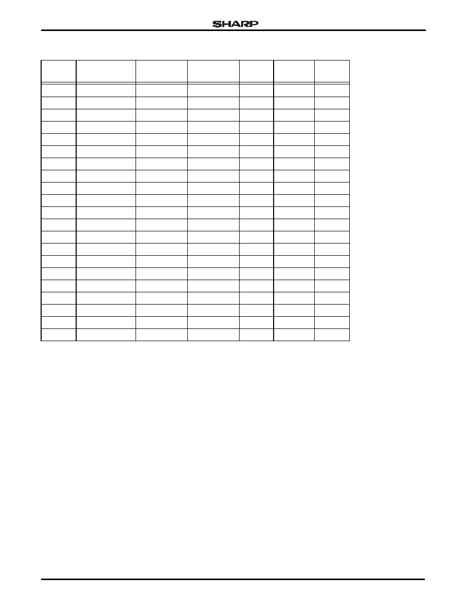
Table 2. LH79520 Numerical Pin List (Cont'd)
PIN NO.
FUNCTION AT
RESET
FUNCTION 2 FUNCTION 3
TYPE
5
OUTPUT
DRIVE
7
NOTES
System-on-Chip
LH79520
Preliminary Data Sheet
9/10/03
13
NOTES:
1. Input with internal pull-up.
2. Input with internal pull-down.
3. Output is for crystal oscilator only, no drive capability.
4. Input with Schmitt Trigger.
5. I/O = Input/Output.
6. Software should avoid enabling the INT5 and DREQ1 functions simultaneously.
7. Output Drive Values shown are MAX. See `DC Specifications'.
8. Crystal Oscillator Inputs should be driven to a maximum of 1.8 V ± 10%.
156
PA5
CLKOUT
I/O
8 mA
157
PWM1
DEOT1
Output
4 mA
158
VSSC
Ground
None
159
PA4
UARTTX1
I/O
4 mA
160
PA3
UARTRX1
I/O
2 mA
4
161
VDD
Power
None
162
UARTIRTX0
UARTTX0
Output
4 mA
163
UARTIRRX0
UARTRX0
Input
None
4
164
PA2
SSPFRM
I/O
4 mA
165
PA1
SSPCLK
I/O
4 mA
166
PA0
SSPEN
I/O
4 mA
167
SSPTX
UARTTX2
Output
4 mA
168
VSS
Ground
None
169
SSPRX
UARTRX2
Input
None
4
170
TMS
Input
None
1, 4
171
TDO
Output
4 mA
172
TDI
Input
None
1, 4
173
TCLK
Input
None
174
nTRST
Input
None
1, 4
175
TEST1
Input
None
2
176
TEST2
Input
None
2
Table 2. LH79520 Numerical Pin List (Cont'd)
PIN NO.
FUNCTION AT
RESET
FUNCTION 2 FUNCTION 3
TYPE
5
OUTPUT
DRIVE
7
NOTES

LH79520
System-on-Chip
14
9/10/03
Preliminary Data Sheet
NOTES:
1. The Intensity bit is identically generated for all three colors.
2. MUSTN = Monochrome Upper data bit for STN panel.
3. MLSTN = Monochrome Lower data bit for STN panel.
4. CUSTN = Color Upper data bit for STN panel.
5. CLSTN = Color Lower data bit for STN panel.
6. Connect to the LSB of the Red, Green, and Blue inputs of a 6:6:6 panel.
7. Recommended hookups for TFT 5:5:5 + Intensity and 5:6:5 are shown.
This wiring requires the BGR bit in the LCDControl Register to be 0.
Table 3. LCD Data Multiplexing
PIN
NO.
LCD DATA
SIGNAL
STN
ALL TFT:
5:5:5+I
ALL TFT:
5:6:5
ALL TFT:
PALETTE
DATA OR
6-BIT DIRECT
MONO 4-BIT
MONO 8-BIT
COLOR
SINGLE
PANEL
DUAL
PANEL
SINGLE
PANEL
DUAL
PANEL
SINGLE
PANEL
DUAL
PANEL
130
LCDVD17
BLUE4
BLUE3
BIT 14
132
LCDVD16
BLUE3
BLUE2
BIT 13
139
LCDVD15
MLSTN7
CLSTN7
BLUE2
BLUE1
BIT 12
140
LCDVD14
MLSTN6
CLSTN6
BLUE1
BLUE0
BIT 11
141
LCDVD13
MLSTN5
CLSTN5
BLUE0
GREEN5
BIT 10
142
LCDVD12
MLSTN4
CLSTN4
114
LCDVD11
MLSTN3
MLSTN3
CLSTN3
GREEN4
GREEN4
BIT 9
115
LCDVD10
MLSTN2
MLSTN2
CLSTN2
GREEN3
GREEN3
BIT 8
116
LCDVD9
MLSTN1
MLSTN1
CLSTN1
GREEN2
GREEN2
BIT 7
117
LCDVD8
MLSTN0
MLSTN0
CLSTN0
GREEN1
GREEN1
BIT 6
118
LCDVD7
MUSTN7 MUSTN7 CUSTN7 CUSTN7 GREEN0
GREEN0
BIT 5
119
LCDVD6
MUSTN6 MUSTN6 CUSTN6 CUSTN6
121
LCDVD5
MUSTN5 MUSTN5 CUSTN5 CUSTN5
RED4
RED4
BIT 4
122
LCDVD4
MUSTN4 MUSTN4 CUSTN4 CUSTN4
RED3
RED3
BIT 3
123
LCDVD3
MUSTN3 MUSTN3 MUSTN3 MUSTN3 CUSTN3 CUSTN3
RED2
RED2
BIT 2
124
LCDVD2
MUSTN2 MUSTN2 MUSTN2 MUSTN2 CUSTN2 CUSTN2
RED1
RED1
BIT 1
126
LCDVD1
MUSTN1 MUSTN1 MUSTN1 MUSTN1 CUSTN1 CUSTN1
RED0
RED0
BIT 0
127
LCDVD0
MUSTN0 MUSTN0 MUSTN0 MUSTN0 CUSTN0 CUSTN0 Intensity
6
BLUE4
BIT 15

System-on-Chip
LH79520
Preliminary Data Sheet
9/10/03
15
SYSTEM DESCRIPTIONS
ARM720T Processor
The LH79520 microcontroller features the ARM720T
cached core with an Advanced High-Performance Bus
(AHB) interface. The ARM720T features:
∑ 32-bit ARM7TDMITM RISC Core
∑ 8KB Cache
∑ MMU (Windows CE enabled)
The processor is a member of the ARM7T family of
processors. For more information, see the ARM docu-
ment, `ARM720T (Rev 3) Technical Reference Manual',
available on Sharp's website at www.sharpsma.com.
The LH79520 MMU provides a means to map Phys-
ical Memory (PA) addresses to virtual memory
addresses. This allows physical memory, which is con-
strained by hardware to specific addresses, to be reor-
ganized at addresses identified by the user. These user
identified locations are called Virtual Addresses (VA).
When the MMU is enabled, Code and Data must be
built, loaded, and executed using Virtual Addresses
which the MMU translates to Physical Addresses. In
addition, the user may implement a memory protection
scheme by using the features of the MMU. Address
translation and memory protection services provided
by the MMU are controlled by the user. The MMU is
directly controlled through the System Control Copro-
cessor, Coprocessor 15 (CP15). The MMU is indirectly
controlled by a Translation Table (TT) and Page Tables
(PT) prepared by the user and established using a por-
tion of physical memory dedicated by the user to stor-
ing the TT and PT's.
Figure 3. LH79520 Application Diagram Example
CODEC
TOUCH
SCREEN
CONTR.
DMA
FLASH/
SRAM/
SDRAM
IMAGER
SSP
STN/
TFT/AD-TFT
PIO
IR
PWM
UART
UART
LH79520
MEMORY
CARD
INTERFACE
FLASH
CARD
79520-6A

LH79520
System-on-Chip
16
9/10/03
Preliminary Data Sheet
Memory Architecture
An integrated SDRAM Controller and Static Memory
Controller provide a glueless interface to external
SDRAM, Flash, SRAM, ROM, and burst ROM. Three
remap options for the physical memory are selectable
by software, as shown in Figures 4, 5, and 6. Memory
is exclusively Little Endian.
SDRAM CONTROLLER
The SDRAM Controller provides the interface
between the internal bus and external (off-chip)
SDRAM memory devices (Figure 2).
The SDRAM Controller provides the following features:
∑ Two independently controlled chip selects.
∑ Transfers data between the controller and SDRAM
in quad-word bursts.
∑ Supports both 32-bit and 16-bit SDRAM.
∑ Supports 2K, 4K, and 8K row address memory parts,
i.e. typical 256M, 128M, 64M, and 16M parts, with 8,
16, or 32 DQ bits per device.
∑ Two reset domains allow SDRAM contents to be
preserved over a soft reset.
STATIC MEMORY CONTROLLER (SMC)
The SMC provides the interface between the internal
bus and external (off-chip) memory devices.
The LH79520 boots from 16-bit memory. The SMC
address space is divided into eight memory banks of
64MB each. The SMC supports:
∑ Static Memory-mapped Devices including RAM,
ROM, Flash, and Burst ROM
∑ Asynchronous Operations:
≠ Page Mode Reads for non-clocked memory
≠ Burst Mode Reads for burst mode ROM
∑ 8-, 16-, and 32-bit wide external memory data paths
∑ Independent configuration for up to eight memory
banks, each up to 64MB
∑ Programmable Parameters:
≠ WAIT States (up to 32)
≠ Bus Turnaround Cycles (1 to 16)
≠ Initial and Subsequent Burst Read WAIT State for
Burst ROM Devices.
The Static Memory Controller (SMC) also supports
an nWAIT input that can be used by an external device
to vary the wait time.
DMA Controller
The DMA Controller provides support for DMA-
capable peripherals. The LCD controller uses its own
DMA port, connecting directly to memory for retrieving
display data.
Figure 4. Memory Remap `00' and `11'
Figure 5. Memory Remap `10'
Figure 6. Memory Remap `01'
79520-5
ADVANCED HIGH-PERFORMANCE BUS
PERIPHERALS
ADVANCED PERIPHERAL BUS
PERIPHERALS
RESERVED
EXTERNAL STATIC MEMORY
EXTERNAL STATIC MEMORY
SDRAM
INTERNAL STATIC MEMORY
0xFFFFFFFF
0xFFFF0000
0xFFFC0000
0x80000000
0x60000000
0x40000000
0x20000000
0x00000000
79520-4
ADVANCED HIGH-PERFORMANCE BUS
PERIPHERALS
ADVANCED PERIPHERAL BUS
PERIPHERALS
RESERVED
INTERNAL STATIC MEMORY
EXTERNAL STATIC MEMORY
SDRAM
INTERNAL STATIC MEMORY
0xFFFFFFFF
0xFFFF0000
0xFFFC0000
0x80000000
0x60000000
0x40000000
0x20000000
0x00000000
79520-3
ADVANCED HIGH-PERFORMANCE BUS
PERIPHERALS
ADVANCED PERIPHERAL BUS
PERIPHERALS
RESERVED
SDRAM
EXTERNAL STATIC MEMORY
SDRAM
INTERNAL STATIC MEMORY
0xFFFFFFFF
0xFFFF0000
0xFFFC0000
0x80000000
0x60000000
0x40000000
0x20000000
0x00000000

System-on-Chip
LH79520
Preliminary Data Sheet
9/10/03
17
∑ Simultaneous servicing of up to 4 data streams
∑ Three transfer modes are supported:
≠ Memory to Memory
≠ Peripheral to Memory
≠ Memory to Peripheral
∑ Identical source and destination capabilities
∑ Transfer Size Programmable (Byte, Half-word, Word)
∑ Burst Size Programmable
∑ Address Increment or Address Freeze
∑ Transfer Error indication for each stream via an
interrupt
∑ 16-word FIFO array with pack and unpack logic
Handles all combinations of byte, half-word or word
transfers from input to output.
Color LCD Controller (CLCDC)
The CLCDC provides all the necessary control and
drive signals to interface directly with a variety of color
and monochrome LCD panels.
∑ Supports single and dual scan color and mono-
chrome Super Twisted Nematic (STN) displays with
4- or 8-bit interfaces
∑ Supports Thin Film Transistor (TFT) color displays
∑ Programmable resolution up to 800 ◊ 600
≠ 800 ◊ 600 (16-bit color can only be supported at
65 Hz refresh rates with 800 ◊ 600 resolution).
∑ 15 gray-level mono, 3,375 color STN, and 64 k color
TFT support
∑ 1, 2, or 4 bits-per-pixel (BPP) for monochrome STN
∑ 1-, 2-, 4-, or 8-BPP palettized color displays for color
STN and TFT
∑ True-color non-palettized, for color STN and TFT
∑ Programmable timing for different display panels
∑ 256-entry, 16-bit palette fast-access RAM
∑ Frame, line and pixel clock signals
∑ AC bias signal for STN or data enable signal for
TFT panels
∑ Patented grayscale algorithm
∑ Interrupt Generation Events
∑ Dual 16-deep programmable 32-bit wide FIFOs for
buffering incoming data.
ADVANCED LCD INTERFACE
The Advanced LCD Interface peripheral allows for
direct connection to ultra-thin panels that do not include
a timing ASIC. It converts TFT signals from the Color
LCD controller to provide the proper signals, timing and
levels for direct connection to a panel's Row and Col-
umn drivers for AD-TFT, HR-TFT, or any technology of
panel that allows for a connection of this type. The
Advanced LCD Interface peripheral also provides a
bypass mode that allows the LH79520 to interface to the
built-in timing ASIC in standard TFT and STN panels.
Synchronous Serial Port (SSP)
The SSP is a master-only interface for synchronous
serial communication with slave peripheral devices that
support protocols for Motorola SPI, National Semicon-
ductor MICROWIRE, or Texas Instruments Synchro-
nous Serial Interface.
∑ Master-only operation
∑ Programmable clock rate
∑ Separate transmit FIFO and receive FIFO buffers,
16 bits wide, 8 locations deep
∑ DMA for transmit and receive
∑ Programmable interface protocols: Motorola SPI,
National Semiconductor MICROWIRE, or Texas
Instruments Synchronous Serial Port
∑ Programmable data frame size from 4 to 16 bits
∑ Independent masking of transmit FIFO, receive
FIFO and receive overrun interrupts
∑ Available internal loopback test mode.
Universal Asynchronous
Receiver Transmitter (UART)
The LH79520 incorporates three UARTs.
∑ Programmable use of UART0 or IrDA SIR input/output
∑ Separate 16-byte transmit and receive FIFOs to
reduce CPU interrupts
∑ Programmable FIFO disabling for 1-byte depth
∑ Programmable baud rate generator
∑ Independent masking of transmit FIFO, receive
FIFO, receive timeout and modem status interrupts
∑ False start bit detection
∑ Line Break generation and detection
∑ Fully-programmable serial interface characteristics:
≠ 5-, 6-, 7-, or 8-bit data word length
≠ Even-, odd- or no-parity bit generation and detection
≠ 1 or 2 stop bit generation
∑ IrDA SIR Encode/Decode block, providing:
≠ Programmable use of IrDA SIR or UART0
input/output
≠ Supports data rates up to 115.2 Kbps half-duplex
≠ Programmable internal clock generator, allowing
division of the Reference clock in increments of 1
to 512 for low-power mode bit durations.
LH79520
System-on-Chip
18
9/10/03
Preliminary Data Sheet
VARIATIONS FROM THE 16C550 UART
The UART varies from the industry-standard
16C550 UART device in six ways:
∑ Receive FIFO trigger levels are fixed at 8 bytes
∑ Receive errors are stored in the FIFO, and do not
generate an interrupt.
∑ The internal register map address space and each
register's bit function differ.
The following 16C550 UART features are not sup-
ported:
∑ 1.5 stop bits (1 or 2 stop bits only are supported)
∑ The forcing stick parity function
∑ Independent receive clock.
Pulse Width Modulator (PWM)
∑ Two independent output channels with separate
input clocks
∑ Up to 16-bit resolution
∑ Programmable synchronous mode support
≠ Allows external input to start PWM
∑ Programmable pulse width (duty cycle), interval (fre-
quency), and polarity
≠ Static programming: PWM is stopped
≠ Dynamic programming: PWM is running
≠ Updates duty cycle, frequency, and polarity at the
end of a PWM cycle
≠ Wide programming range.
Vectored Interrupt Controller
The Vectored Interrupt Controller combines the
interrupt request signals from 20 internal and eight
external interrupt sources and applies them, after
masking and prioritization, to the IRQ and FIQ interrupt
inputs of the ARM7TDMI processor core.
The Interrupt Controller incorporates a hardware
interrupt vector logic with programmable priority for up
to 16 interrupt sources. This logic reduces the interrupt
response time for IRQ type interrupts compared to
solutions using software polling to determine the high-
est priority interrupt source. This significantly improves
the real-time capabilities of the LH79520 in embedded
control applications.
∑ 20 internal and eight external interrupt sources
≠ Individually maskable
≠ Status accessible for software polling
∑ IRQ interrupt vector logic for up to 16 channels with
programmable priorities
∑ All of the interrupt channels, with the exception of the
Watchdog Timer interrupt, can be programmed to
generate:
≠ FIQ interrupt request
≠ Non-vectored IRQ interrupt request (software to
poll IRQ source)
≠ Vectored IRQ interrupt request (up to 16 chan-
nels total)
∑ The Watchdog timer can only generate FIQ interrupt
requests
∑ External interrupt inputs programmable
≠ Edge triggered or level triggered
≠ Rising edge/active HIGH or falling edge/active
LOW
The 28 interrupt channels are shown in Table 4.
Table 4. Interrupt Channels
CHANNEL
INTERRUPT SOURCE
0
External Interrupt 0
1
External Interrupt 1
2
External Interrupt 2
3
External Interrupt 3
4
External Interrupt 4
5
External Interrupt 5
6
External Interrupt 6
7
External Interrupt 7
8
Spare Internal Interrupt 0
9
COMRX (used for debug)
10
COMTX (used for debug)
11
SSP RX time-out interrupt SSPRXTO
12
CLCD Combined Interrupt
13
SSP SSPTXINTR
14
SSP SSPRXINTR
15
SSP SSPRORINTR
16
SSP SSPINTR
17
Counter/Timer0
18
Counter/Timer1
19
Counter/Timer2
20
Counter/Timer3
21
UART ch0 Rx
22
UART ch0 Tx
23
UART ch0
24
UART ch1
25
UART ch2
26
DMA Combined
27-29
Unused
30
RTC_ALARM
31
WDT

System-on-Chip
LH79520
Preliminary Data Sheet
9/10/03
19
Reset, Clock, and Power
Controller (RCPC)
The RCPC generates the various clock signals for the
operation of the LH79520 and provides for an orderly
start-up after power-on and during a wake-up from one
of the power saving operating modes. The RCPC allows
the software to individually select the frequency of the
various on-chip clock signals as required to operate the
chip in the most power-efficient mode. It features:
∑ 14.7456 MHz crystal oscillator and PLL for on-chip
Clock generation
∑ External Clock input if on-chip oscillator and PLL are
not used
∑ 32.768 kHz crystal oscillator generating 1 Hz clock
for Real Time Clock
∑ Individually controlled clocks for peripherals and CPU
∑ Clock source for UARTs is selectable between
14.7456 MHz crystal oscillator and external clock
source
∑ Programmable clock prescalers for UARTs and
PWMs
∑ Five global power control modes are available:
≠ Active
≠ Standby
≠ Sleep
≠ Stop1
≠ Stop2
∑ CPU and Bus clock frequency can be changed
on the fly
∑ Selectable clock output
∑ Hardware reset (nRESETIN) and software reset.
Table 5. Clock and Enable States for Different Power Modes
(Using On-chip Oscillator and PLL)
FUNCTION
ACTIVE
STANDBY
SLEEP
STOP1
STOP2
14.7456 MHz Oscillator
ON
ON
ON
ON
OFF
PLL
ON
ON
ON
OFF
OFF
Peripheral Clock
ON
ON
OFF
OFF
OFF
CPU Clock
ON
OFF
OFF
OFF
OFF

LH79520
System-on-Chip
20
9/10/03
Preliminary Data Sheet
Real Time Clock
The RTC can provide a basic alarm function or long
time base counter. This is achieved by generating an
interrupt signal after counting for a programmed num-
ber of cycles of RTC input. Counting in one-second
intervals is achieved by the use of a 1 Hz clock input to
the RTC.
The features of the RTC are:
∑ 32-bit up counter with programmable load
∑ Programmable 32-bit match compare register
∑ Software maskable interrupt when counter and com-
pare registers are identical.
RTC input clock sources:
∑ PLL clock
∑ 32.768 kHz clock
∑ 1 Hz clock (default).
Watchdog Timer
The Watchdog Timer provides hardware protection
against malfunctions. It is a programmable timer to be
reset by software at regular intervals. Failure to reset
the timer will cause a FIQ interrupt. Failure to service
the FIQ interrupt will then generate a System Reset.
The features of the Watchdog Timer are:
∑ Driven by the bus clock
∑ 16 programmable time-out periods: 2
16
through 2
31
clock cycles
∑ Generates a system reset (resets LH79520) or a FIQ
Interrupt whenever a time-out period is reached
∑ Software enable, lockout, and counter-reset mecha-
nisms add security against inadvertent writes
∑ Protection mechanism guards against interrupt-ser-
vice failure:
≠ The first WDT time-out triggers FIQ and asserts
nWDFIQ status flag
≠ If FIQ service routine fails to clear nWDFIQ, then
the next WDT time-out triggers a soft reset.
Timer
The LH79520 incorporates two Timer modules,
each comprising two 16-bit independently programma-
ble timers. This gives a total of four independent timers.
∑ Each timer has two operating modes:
≠ Free-running mode: After reaching 0x0000 the
timer wraps around to 0xFFFF and generates an
interrupt request. It continues to count down from
0xFFFF.
≠ Periodic timer mode: After reaching 0x0000 the
timer is automatically reloaded with its pro-
grammed value and generates an interrupt re-
quest. It continues to count down from the
loaded value.
∑ Each timer contains a programmable pre-scaler:
≠ Bus clock divided by 1, 16, or 256
∑ Timers can be cascaded to achieve longer timing
periods
∑ Carry-out of higher-order timer provides clock signal
for next lower order timer
∑ Possible timing ranges:
≠ 2
15
(single timer)
≠ 2
31
(two timers cascaded)
≠ 2
47
(three timers cascaded)
≠ 2
63
(four timers cascaded)
∑ Output signal of lowest order timer is externally avail-
able as CTOUT1B signal.
Input/Output Configuration System
The registers provided by the IOCON System allow
the user to directly control the pin multiplexing of the
device; by setting or clearing bits in a set of registers, the
user can configure the LH79520 for peripheral devices.
General Purpose Input/Output (GPIO)
The LH79520 provides up to 64 bits of programma-
ble input/output. These eight 8-bit ports are Ports A
through H, and are multiplexed with other signals.
∑ Individually programmable input/output pins
∑ All I/O ports default to Input on power-up.
System-on-Chip
LH79520
Preliminary Data Sheet
9/10/03
21
ELECTRICAL SPECIFICATIONS
Absolute Maximum Ratings
NOTE: These stress ratings are only for transient conditions. Oper-
ation at or beyond absolute maximum rating conditions may
affect reliability and cause permanent damage to the device.
Recommended Operating Conditions
NOTE: *Using 14.7456 MHz Input Crystal and On-Chip PLL. Functional to DC when using external clock.
PARAMETER
SYMBOL
RATING
UNIT
DC Core Supply Voltage
VDDC
-0.3 to 2.4
V
DC I/O Supply Voltage
VDD
-0.3 to 4.6
V
DC Analog Supply Voltage
VDDA
-0.3 to 2.4
V
Storage Temperature
TSTG
-55 to +125
∞C
PARAMETER
MINIMUM
TYPICAL
MAXIMUM
DC Core Supply Voltage (VDDC)
1.62 V
1.8 V
1.98 V
DC I/O Supply Voltage (VDD)
3.0 V
3.3 V
3.6 V
DC Analog Supply Voltage (VDDA)
1.62 V
1.8 V
1.98 V
Clock Frequency*
10 MHz
77.4144 MHz
Commercial Operating Temperature
0∞C
25∞C
+70∞C
Industrial Operating Temperature
-40∞C
25∞C
+85∞C
LH79520
System-on-Chip
22
9/10/03
Preliminary Data Sheet
DC/AC SPECIFICATIONS (COMMERCIAL)
Unless otherwise noted, all data provided under
commercial DC specifications are based on 0∞C to
+70∞C, VDDC = 1.62 V to 1.98 V, VDD = 3.0 V to 3.6 V,
VDDA = 1.62 V to 1.98 V.
DC Specifications (Commercial)
NOTES:
1. Table 2 details each pin's buffer type.
2. Running Typical Application over operating range.
3. Current measured with CPU stopped and all peripherals enabled.
AC Test Conditions
SYMBOL
PARAMETER
MIN. TYP. MAX. UNIT
CONDITIONS
NOTES
VIH
CMOS input HIGH voltage
2.0
5.5
V
VIL
CMOS input LOW voltage
0.8
V
VIT+
Positive Input thrueshold voltage (Schmitt trigger pins)
1.60
V
1
VIT-
Negative Input threshold voltage (Schmitt trigger pins)
1.20
V
VHYST
Schmitt trigger hysteresis
0.40
V
VIT+ ≠ VIT-
VOH
CMOS output HIGH voltage
2.6
V
IOH = -50
µ
A
1
Output drive (2 mA type)
2.6
V
IOH = -2 mA
Output drive (4 mA type)
2.6
V
IOH = -4 mA
Output drive (8 mA type)
2.6
V
IOH = -8 mA
VOL
CMOS output LOW voltage
0.4
V
IOL = 50
µ
A
1
Output drive (2 mA type)
0.4
V
IOL = 2 mA
Output drive (4 mA type)
0.4
V
IOL = 4 mA
Output drive (8 mA type)
0.4
V
IOL = 8 mA
XTAL32IN
External Clock Input
1.62
1.8
1.98
V
XTALIN
External Clock Input
1.62
1.8
1.98
V
IIN
Input leakage current
-10
10
µ
A
VIN = VDD or GND
IOZ
Output tri-state leakage current
-10
10
µ
A
VOUT = VDD or GND
IACTIVE
Active current
43.5
55
mA
2
ISTANDBY Standby current
27.5
35
mA
2, 3
ISLEEP
Sleep current
3.9
5.5
mA
ISTOP1
Stop1 current
500
µ
A
ISTOP2
Stop2 current (RTC ON)
34
µ
A
ISTOP2
Stop2 current (RTC OFF)
18
µ
A
CIN
Input Capacitance
4
pF
COUT
Output Capacitance
4
pF
PARAMETER
RATING
UNIT
Supply Voltage (VDD)
3.0 to 3.6
V
Core Voltage (VDDC)
1.62 to 1.98
V
Input Pulse Levels
VSS to VDD
V
Input Rise and Fall Times
2
ns
Input and Output Timing Ref. Levels
VDD/2
V

System-on-Chip
LH79520
Preliminary Data Sheet
9/10/03
23
AC Specifications
All signals described in Table 6 relate to transitions
after a reference clock signal. The illustration in Figure
7 represents all cases of these sets of measurement
parameters; except for the Asynchronous Memory
Interface -- which are referenced to Address Valid.
The reference clock signals in this design are:
∑ HCLK, the System Bus clock
∑ PCLK, the Peripheral Bus clock (locked to HCLK in
the LH79520)
∑ SSPCLK, the Synchronous Serial Interface clock
∑ UARTCLK, the UART Interface clock
∑ LCDDCLK, the LCD Data clock from the
LCD Controller
∑ and SDCLK, the SDRAM clock.
All signal transitions are measured from the 50%
point of the clock to the 50% point of the signal. See
Figure 7.
For outputs from the LH79520, tOVXXX (e.g. tOVA)
represents the amount of time for the output to become
valid from the rising edge of the reference clock signal.
Maximum requirements for tOVXXX are shown in
Table 6.
The signal tOHXXX (e.g. tOHA) represents the
amount of time the output will be held valid from the ris-
ing edge of the reference clock signal. Minimum
requirements for tOHXXX are listed in Table 6.
For Inputs, tISXXX (e.g. tISD) represents the
amount of time the input signal must be valid before the
rising edge of the clock signal. Minimum requirements
for tISXXX are shown in Table 6.
The signal tIHXXX (e.g. tIHD) represents the
amount of time the output must be held valid from the
rising edge of the reference clock signal. Minimum
requirements are shown in Table 6.
Figure 7. LH79520 Signal Timing
REFERENCE
CLOCK
OUTPUT
SIGNAL (O)
INPUT
SIGNAL (I)
tOVXXX
tOHXXX
tISXXX tIHXXX
79520-34
LH79520
System-on-Chip
24
9/10/03
Preliminary Data Sheet
Table 6. AC Signal Characteristics (Commercial)
SIGNAL
TYPE LOAD DRIVE
SYMBOL
MIN.
MAX.
DESCRIPTION
ASYNCHRONOUS MEMORY INTERFACE SIGNALS
D[31:0]
Output 50 pF
8 mA
tOVD
tHCLK + 6 ns
Data Output Valid, following
Address Valid
tOHD
3 ◊ tHCLK - 6 ns
Data Output Invalid, following
Address Valid
Input
tIDD
2 ◊ tHCLK ≠ 18 ns
Data Input Valid, following
Address Valid
nCS6 - nCS0 Output 30 pF
8 mA
tOVCS
tHCLK + 6 ns
Chip Select Output Valid,
following Address Valid
tOHCS
3 ◊ tHCLK - 6 ns
Chip Select Output Invalid,
following Address Valid
nBLE[3:0] Output 30
pF
8
mA
tOVBE
tHCLK + 10 ns
Byte Lane Enable Valid,
following Address Valid
tOHBEW
2 ◊ tHCLK - 6 ns
Byte Lane Enable Invalid, follow-
ing Address Valid; Write Cycle
tOHBER
3 ◊ tHCLK - 6 ns
Byte Lane Enable Invalid, follow-
ing Address Valid; Read Cycle
nWE
Output 30 pF
8 mA
tOVWE
tHCLK + 10 ns
Write Enable Valid, following
Address Valid
tOHWE
2 ◊ tHCLK - 6 ns
Write Enable Invalid, following
Address Valid
nOE Output 30
pF
8
mA
tOVOE
tHCLK + 10 ns
Ouput Enable Valid, following
Address Valid
tOHOE
3 ◊ tHCLK - 6 ns
Ouput Enable Invalid, following
Address Valid
nWAIT
Input
tISWAIT
2 ◊ tHCLK ≠ 18 ns
WAIT Input Valid, following
Address Valid
SYNCHRONOUS MEMORY INTERFACE SIGNALS
A[25:0]
Ouput
50 pF
8 mA
tOVA
10.5 ns
Address Valid
D[31:0]
Output 50 pF
8 mA
tOVD
11 ns
Output Data Valid
tOHD
1.2 ns
Output Data Hold
Input
tISD
5 ns
Input Data Setup
tIDD
1.5 ns
Input Data Hold
nCAS
Output 50 pF
8 mA
tOVCA
10.5 ns
CAS Valid
tOHCA
2 ns
CAS Hold
nRAS
Output 50 pF
8 mA
tOVRA
10.5 ns
RAS Valid
tOHRA
2 ns
RAS Hold
nSDWE
Output 30 pF
8 mA
tOVSDW
10.5 ns
SDWE Write Enable Valid
tOHSDW
2 ns
SDWE Write Enable Hold
SDCKE
Output 30 pF
8 mA
tOVC0
10.5 ns
SDCKE Clock Enable Valid
tOHC0
2 ns
SDCKE Clock Enable Hold
DQM[3:0] Output 30
pF
8
mA
tOVDQ
10.5 ns
DQM Data Mask Valid
tOHDQ
2 ns
DQM Data Mask Hold
nSDCS[1:0] Output 30
pF
8
mA
tOVSC
10.5 ns
SDCS Data Mask Valid
tOHSC
2 ns
SDCS Data Mask Hold
SDCLK
Output 30 pF
8 mA
tSDCLK
19.37 ns
SDRAM Clock Period

System-on-Chip
LH79520
Preliminary Data Sheet
9/10/03
25
NOTES:
1. INTR[5:0] are asynchronous signals. Interrupts must be held Active until serviced in Level Sensitive Mode,
and held Active for a minimum of 20 ns in Edge Sensitive Mode.
2. DACK0, nDACK1 and DREQ[1:0] are asynchronous signals. They must be held Active until serviced,
for a minimum of 20 ns.
SYNCHRONOUS SERIAL PORT (SSP)
SSPFRM
Output 50 pF
2 mA
tOVSSPFRM
14 ns
tOVSSPFRM Output Valid,
Referenced to SSPCLK
SSPENB
Output 50 pF
2 mA
tOVSSPENB
14ns
tOVSSPENB Output Valid,
Referenced to SSPCLK
SSPTX
Output 50 pF
2 mA
tOVSSPOUT
14ns
SSP Transmit Valid
SSPRX
Input
tISSSPIN
17 ns
SSP Receive Setup
INTERRUPTS
INTR[5:0]
Input
Note 1
Table 6. AC Signal Characteristics (Commercial) (Cont'd)
SIGNAL
TYPE LOAD DRIVE
SYMBOL
MIN.
MAX.
DESCRIPTION
LH79520
System-on-Chip
26
9/10/03
Preliminary Data Sheet
DC/AC SPECIFICATIONS (INDUSTRIAL)
Unless otherwise noted, all data provided under
industrial DC specifications are based on -40∞C to
+85∞C, VDDC = 1.62 V to 1.98 V, VDD = 3.0 V to 3.6 V,
VDDA = 1.62 V to 1.98 V.
DC Specifications (Industrial)
NOTES:
1. Table 2 details each pin's buffer type.
2. Running Typical Application over operating range.
3. Current measured with CPU stopped and all peripherals enabled.
AC Test Conditions
SYMBOL
PARAMETER
MIN. TYP. MAX. UNIT
CONDITIONS
NOTES
VIH
CMOS input HIGH voltage
2.0
5.5
V
VIL
CMOS input LOW voltage
0.8
V
VIT+
Positive Input thrueshold voltage (Schmitt trigger pins)
1.60
V
1
VIT-
Negative Input threshold voltage (Schmitt trigger pins)
1.20
V
VHST
Schmitt trigger hysteresis
0.40
V
VIT+ ≠ VIT-
VOH
CMOS output HIGH voltage
2.6
V
IOH = -50
µ
A
1
Output drive (2 mA type)
2.6
V
IOH = -2 mA
Output drive (4 mA type)
2.6
V
IOH = -4 mA
Output drive (8 mA type)
2.6
V
IOH = -8 mA
VOL
CMOS output LOW voltage
0.4
V
IOL = 50
µ
A
1
Output drive (2 mA type)
0.4
V
IOL = 2 mA
Output drive (4 mA type)
0.4
V
IOL = 4 mA
Output drive (8 mA type)
0.4
V
IOL = 8 mA
XTAL32IN
External Clock Input
1.62
1.8
1.98
V
XTALIN
External Clock Input
1.62
1.8
1.98
V
IIN
Input leakage current
-10
10
µ
A
VIN = VDD or GND
IOZ
Output tri-state leakage current
-10
10
µ
A
VOUT = VDD or GND
IACTIVE
Active current
43.5
55
mA
2
ISTANDBY Standby current
27.5
35
mA
2, 3
ISLEEP
Sleep current
3.9
5.5
mA
ISTOP1
Stop1 current
500
µ
A
ISTOP2
Stop2 current (RTC ON)
34
µ
A
ISTOP2
Stop2 current (RTC OFF)
18
µ
A
CIN
Input Capacitance
4
pF
COUT
Output Capacitance
4
pF
PARAMETER
RATING
UNIT
Supply Voltage (VDD)
3.0 to 3.6
V
Core Voltage (VDDC)
1.62 to 1.98
V
Input Pulse Levels
VSS to VDD
V
Input Rise and Fall Times
2
ns
Input and Output Timing Ref. Levels
VDD/2
V

System-on-Chip
LH79520
Preliminary Data Sheet
9/10/03
27
AC Specifications (Industrial)
Table 7. AC Signal Characteristics (Industrial)
SIGNAL
TYPE LOAD DRIVE
SYMBOL
MIN.
MAX.
DESCRIPTION
ASYNCHRONOUS MEMORY INTERFACE SIGNALS
D[31:0]
Output 50 pF
8 mA
tOVD
tHCLK + 6.5 ns
Data Output Valid, following
Address Valid
tOHD
3 ◊ tHCLK - 6 ns
Data Output Invalid, following
Address Valid
Input
tIDD
2 ◊ tHCLK ≠ 18 ns
Data Input Valid, following
Address Valid
nCS6 - nCS0 Output 30 pF
8 mA
tOVCS
tHCLK + 6 ns
Chip Select Output Valid,
following Address Valid
tOHCS
3 ◊ tHCLK - 6 ns
Chip Select Output Invalid,
following Address Valid
nBLE[3:0] Output 30
pF
8
mA
tOVBE
tHCLK + 10 ns
Byte Lane Enable Valid,
following Address Valid
tOHBEW
2 ◊ tHCLK - 6 ns
Byte Lane Enable Invalid, follow-
ing Address Valid; Write Cycle
tOHBER
3 ◊ tHCLK - 6 ns
Byte Lane Enable Invalid, follow-
ing Address Valid; Read Cycle
nWE
Output 30 pF
8 mA
tOVWE
tHCLK + 10 ns
Write Enable Valid, following
Address Valid
tOHWE
2 ◊ tHCLK - 6 ns
Write Enable Invalid, following
Address Valid
nOE Output 30
pF
8
mA
tOVOE
tHCLK + 10 ns
Ouput Enable Valid, following
Address Valid
tOHOE
3 ◊ tHCLK - 6 ns
Ouput Enable Invalid, following
Address Valid
nWAIT
Input
tISWAIT
2 ◊ tHCLK ≠ 18 ns
WAIT Input Valid, following
Address Valid
SYNCHRONOUS MEMORY INTERFACE SIGNALS
A[25:0]
Ouput
50 pF
8 mA
tOVA
10.5 ns
Address Valid
D[31:0]
Output 50 pF
8 mA
tOVD
11.5 ns
Output Data Valid
tOHD
1.2 ns
Output Data Hold
Input
tISD
5 ns
Input Data Setup
tIDD
1.5 ns
Input Data Hold
nCAS
Output 50 pF
8 mA
tOVCA
11 ns
CAS Valid
tOHCA
2 ns
CAS Hold
nRAS
Output 50 pF
8 mA
tOVRA
11 ns
RAS Valid
tOHRA
2 ns
RAS Hold
nSDWE
Output 30 pF
8 mA
tOVSDW
11 ns
SDWE Write Enable Valid
tOHSDW
2 ns
SDWE Write Enable Hold
SDCKE
Output 30 pF
8 mA
tOVC0
11 ns
SDCKE Clock Enable Valid
tOHC0
2 ns
SDCKE Clock Enable Hold
DQM[3:0] Output 30
pF
8
mA
tOVDQ
11 ns
DQM Data Mask Valid
tOHDQ
2 ns
DQM Data Mask Hold
nSDCS[1:0] Output 30
pF
8
mA
tOVSC
11 ns
SDCS Data Mask Valid
tOHSC
2 ns
SDCS Data Mask Hold
SDCLK
Output 30 pF
8 mA
tSDCLK
19.37 ns
SDRAM Clock Period
LH79520
System-on-Chip
28
9/10/03
Preliminary Data Sheet
NOTES:
1. INTR[5:0] are asynchronous signals. Interrupts must be held Active until serviced in Level Sensitive Mode,
and held Active for a minimum of 20 ns in Edge Sensitive Mode.
2. DACK0, nDACK1 and DREQ[1:0] are asynchronous signals. They must be held Active until serviced,
for a minimum of 20 ns.
SYNCHRONOUS SERIAL PORT (SSP)
SSPFRM
Output 50 pF
2 mA
tOVSSPFRM
14 ns
tOVSSPFRM Output Valid,
Referenced to SSPCLK
SSPENB
Output 50 pF
2 mA
tOVSSPENB
14ns
tOVSSPENB Output Valid,
Referenced to SSPCLK
SSPTX
Output 50 pF
2 mA
tOVSSPOUT
14ns
SSP Transmit Valid
SSPRX
Input
tISSSPIN
17 ns
SSP Receive Setup
INTERRUPTS
INTR[5:0]
Input
Note 1
Table 7. AC Signal Characteristics (Cont'd)(Industrial)
SIGNAL
TYPE LOAD DRIVE
SYMBOL
MIN.
MAX.
DESCRIPTION

System-on-Chip
LH79520
Preliminary Data Sheet
9/10/03
29
EXTERNAL CLOCKS
NOTES:
1. PCLK is the period chosen for the internal peripheral
clock domain.
2. MAX. period is DC. See `Recommended Operating Conditions'.
Table 8. External Clocks AC Specifications
SYMBOL
DESCRIPTION
MIN.
UNIT
tCLKIN
CLKIN Period
6.66
ns
tCLKINH
CLKIN HIGH Time
2.8
ns
tCLKINL
CLKIN LOW TIme
2.8
ns
tSSPCLK
SSPCLK Period
1
PCLK
tSSPCLKH
SSPCLK HIGH Time
0.4
PCLK
tSSPCLKL
SSPCLK LOW Time
0.4
PCLK
tUCLK
UCLK
1
PCLK
tUCLKH
UCLK HIGH Time
0.4
PCLK
tUCLKL
UCLK LOW Time
0.4
PCLK
Figure 8. External Clock AC Timing
tCLKINL
tCLKIN
tCLKINH
79520-57
Figure 9. Synchronous Serial I/F Clocks AC Timing
Figure 10. External UARTs/SIR Clock AC Timing
tSSPCLK
tSSPCLKL
79520-58
tSSPCLKH
79520-59
tUCLKH
tUCLK
tUCLKL

LH79520
System-on-Chip
30
9/10/03
Preliminary Data Sheet
Static Memory Controller Waveforms
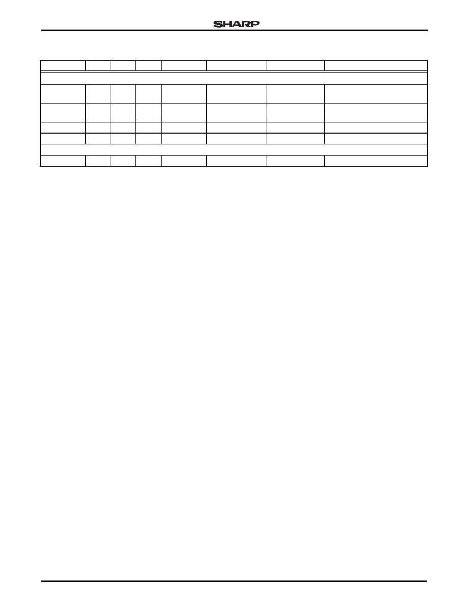
nWAIT INPUT
The Static Memory Controller (SMC) supports an
nWAIT input that can be used by an external device to
extend the wait time during a memory access. The
SMC samples nWAIT at the beginning of at the begin-
ning of each system clock cycle. The system clock
cycle in which the nCSx signal is asserted counts as
the first wait state. See Figure 11.
The SMC recognizes that nWAIT is active within 2
clock cycles after it has been asserted. To assure that
the current access (read or write) will be extended by
nWAIT, at least two wait states must be programmed
for this bank of memory. If N wait states are pro-
grammed, then the Static Memory Controller (SMC)
holds this state for N system clocks, or until the SMC
detects that nWAIT is inactive, whichever occurs last.
As the number of wait states programmed increases,
the amount of delay before nWAIT must be asserted
also increases. If only 2 wait states are programmed,
then nWAIT must be asserted in the clock cycle imme-
diately following the clock cycle during which the nCSx
signal is asserted. Once the SMC detects that the
external device has deactivated nWAIT, the SMC will
complete its access in 3 system clock cycles.
The formula for the allowable delay between assert-
ing nCSx and asserting nWAIT is:
tASSERT = (system clock period) ◊ (Wait States - 1)
(where Wait States is from 2 to 31.)
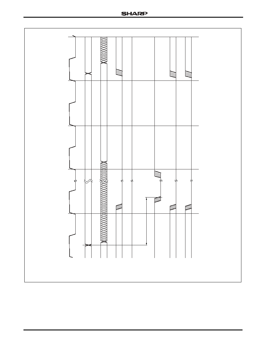
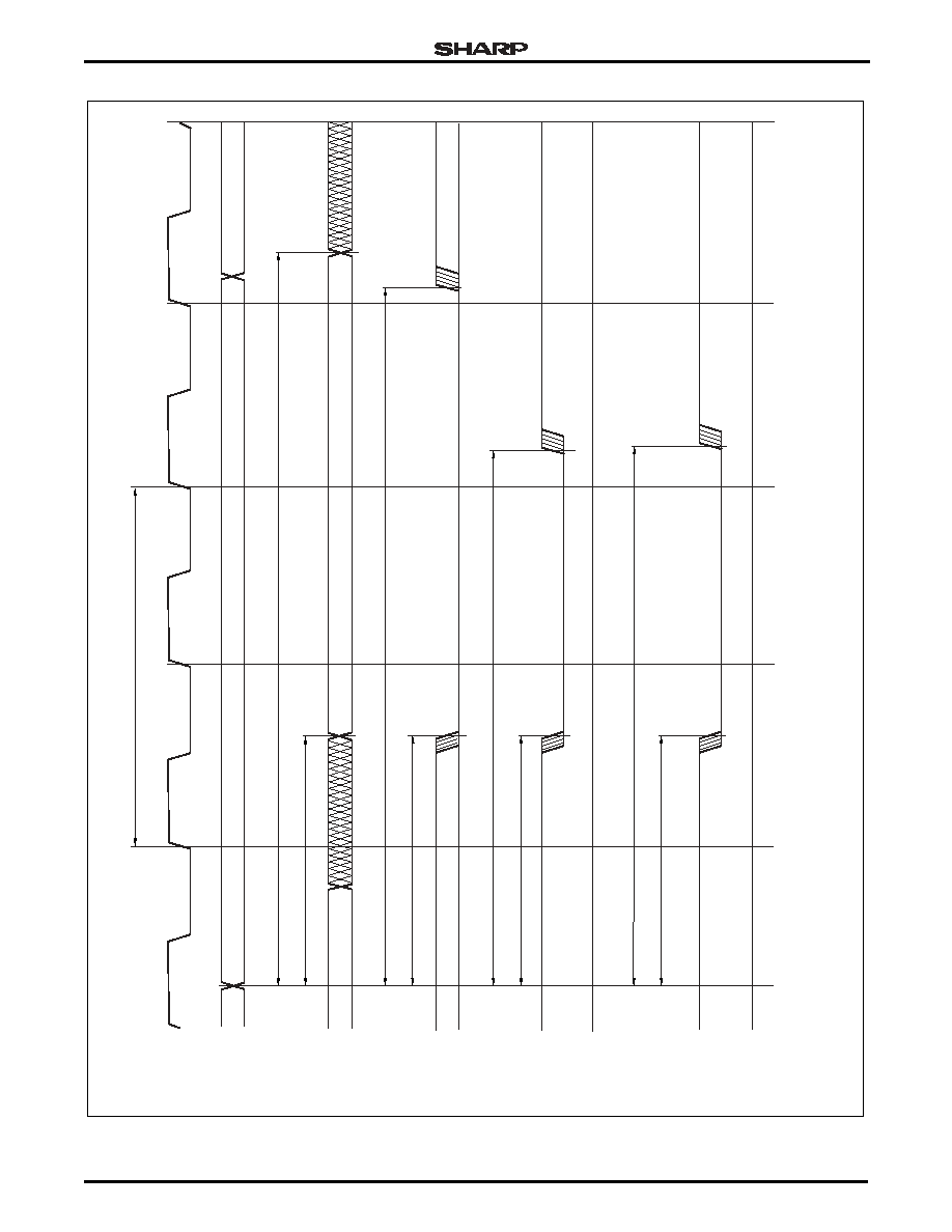
READ AND WRITE WAVEFORMS
Figure 12 shows the waveform and timing for an
External Static Memory Write. Figure 13 shows the
waveform and timing for an External Static Memory
Read, with one Wait State. Figure 14 shows the wave-
form and timing for an External Static Memory Read,
with two Wait States.
System-on-Chip
LH79520
Preliminary Data Sheet
9/10/03
31
Figure 11. nWait Assertion
HCLK
D[31:0]
A[23:0]
ADDRESS
D
ATA
nCSx
nOE
nWE
nW
AIT
nBLE[1:0]
79520-108
NO
TES:
1.
HCLK is an inter
nal signal, pro
vided f
or ref
erence only
.
2. The corresponding b
yte lane enab
le(s) become activ
e
.
(See Note 1)
(See Note 2)
tISW
AIT

LH79520
System-on-Chip
32
9/10/03
Preliminary Data Sheet
Figure 12. External Static Memory Write, One Wait State
79520-30
HCLK
A[23:0]
D[31:0]
nCSx
nWE
nW
AIT
nBLE[1:0]
nOE
tOHWE
tO
VWE
1 W
AIT
ST
A
T
E
tO
VD
tOHD
tO
VCS
tOHCS
D
ATA
ADDRESS
tOHBEW
tO
VBE
NO
TES:
1.
HCLK is an inter
nal signal, pro
vided f
or ref
erence only
.
2.
The corresponding b
yte lane enab
le(s) become activ
e
.
3.
1 HCLK of nWE is the minim
um amount of asser
tion time necessar
y bef
ore adding a
W
ait state
.
(See Note 1)
(See Note 2)

System-on-Chip
LH79520
Preliminary Data Sheet
9/10/03
33
Figure 13. External Static Memory Read, One Wait State
1 W
AIT
ST
A
T
E
ADDRESS
D
ATA
tIDD
tO
VCS
tO
VBE
tO
V
O
E
tOHOE
tOHCS
tOHBER
HCLK
A[23:0]
D[31:0]
nCSx
nWE
nW
AIT
nOE
nBLE[1:0]
79520-31
NO
TES:
1.
HCLK is an inter
nal signal, pro
vided f
or ref
erence only
.
2. The corresponding b
yte lane enab
le(s) become activ
e
.
(See Note 1)
(See Note 2)
LH79520
System-on-Chip
34
9/10/03
Preliminary Data Sheet
Figure 14. External Static Memory Write, Two Wait States
HCLK
(See Note 1)
A[23:0]
D[31:0]
nCSx
nWE
nW
AIT
nBLE[1:0]
(See Note 2)
nOE
tOHWE + 1 HCLK
tO
VWE
2 W
AIT
ST
A
TES
tO
VD
tOHD + 1 HCLK
tO
VCS
tOHCS + 1 HCLK
D
ATA
ADDRESS
tOHBEW + 1 HCLK
tO
VBE
NO
TES:
1.
HCLK is an inter
nal signal, pro
vided f
or ref
erence only
.
2. The corresponding b
yte lane enab
le(s) become activ
e
.
79520-32

System-on-Chip
LH79520
Preliminary Data Sheet
9/10/03
35
Figure 15. Synchronous Serial Port Waveform
SSPCLK
SSPFRM
SSPTX
SSPRX
tO
VSSPFRM
tO
VSSPTX
tISSPRX
79520-171

LH79520
System-on-Chip
36
9/10/03
Preliminary Data Sheet
SDRAM Memory Controller Waveforms
Figure 16 shows the waveform and timing for an
SDRAM Burst Read (page already open). Figure 17
shows the waveform and timing for SDRAM to Activate
a Bank and Write.
Figure 16. SDRAM Burst Read
Figure 17. SDRAM Bank Activate and Write
tSDCLK
LH79520-35
A[15:0]
D[31:0]
NOTES:
1. SDRAMcmd is the combination of nRAS, nCAS, nSDWE, and nSDCS(X).
2. tOVXXX represents tOVRA, tOVCA, tOVSDW, or tOVSC.
3. tOHXXX represents tOHRA, tOHCA, tOHSDW, or tOHSC.
4. nDQM is LOW.
5. SDCKE is HIGH.
SCLK
SDRAMcmd
tOVXXX
tOV
tOHXXX
READ
BANK,
COLUMN
tOVA
tISD tIHD
DATA n
DATA n + 1
DATA n + 2
DATA n + 3
79520-36
D[31:0]
SCLK
SDCKE
SDRAMcmd
tSDCLK
tOVC0
tOVXXX
tOVA
tOHXXX
tOVA
NOTES:
1. SDRAMcmd is the combination of nRAS, nCAS, nSDWE, and nSDCS(X).
2. tOVXXX represents tOVRA, tOVCA, tOVSDW, or tOVSC. Refer to the AC timing table.
3. tOHXXX represents tOHRA, tOHCA, tOHSDW, or tOHSC.
4. nDQM is LOW.
ACTIVE
WRITE
DATA
BANK,
ROW
BANK,
COLUMN
tOVD
tOHD
A[15:0]

System-on-Chip
LH79520
Preliminary Data Sheet
9/10/03
37
External DMA Handshake Signal Timing
DREQ TIMING
Once asserted, DREQ0 or DREQ1 must not transi-
tion from LOW to HIGH again until after DACK0 or
nDACK1 has been asserted.
DACK/DEOT TIMING
These timing diagrams indicate when DACK0,
nDACK1, DEOT0 and DEOT1 occur in relation to an
external bus access to/from the external peripheral that
requested the DMA transfer.
The top diagram shows the timing with relation to a
single read or the last word of a burst read from the
requesting peripheral. The bottom diagram shows the
timing with relation to a single write or the last word of
a burst write to the requesting peripheral.
The timing of DACK/DEOT may become unpredict-
able when a Write to SDRAM occurs just prior to a sin-
gle word Write to the requesting peripheral. If the write
buffer is enabled for the SDRAM Controller, this can
cause the DACK/DEOT to occur an indeterminate
number of cycles prior to the actual Write to the
requesting peripheral.
Figure 18. DREQ Timing Restrictions
DREQ
MUST NOT
TRANSITON
DREQ MAY
TRANSITON
tDREQ0L,
tDREQ1L
DREQ0,
DREQ1
DACK0
nDACK1
NOTE: tDREQ0L = DREQ0 LOW Pulse Width = 2 HCLK MIN.
tDREQ1L = DREQ1 LOW Pulse Width = 2 HCLK MIN.
79520-158

LH79520
System-on-Chip
38
9/10/03
Preliminary Data Sheet
Figure 19. Read, from Peripheral to Memory, Burst Size = 1
Figure 20. Write, from Memory to Peripheral, Burst Size = 1
HCLK
(See Note)
A[23:0]
ADDRESS
DATA
D[31:0]
nCSx
nWEN
nBLE[1:0]
nOE
DACK0/
DEOT0/DEOT1
nDACK1
NOTE: * HCLK is an internal signal provided for reference only.
79520-156
HCLK
(See Note)
A[23:0]
D[15:0]
nCSx
nWEN
nBLE[1:0]
nOE
nDACK1
NOTE: * HCLK is an internal signal provided for reference only.
DACK0/
DEOT0/DEOT1
ADDRESS
DATA
79520-157
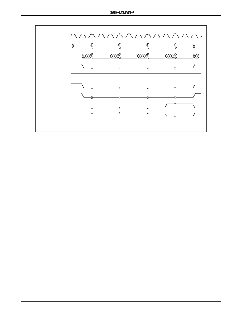
System-on-Chip
LH79520
Preliminary Data Sheet
9/10/03
39
Figure 21. Read, Peripheral to Memory: Peripheral Burst Size = 4
HCLK
*
A[23:0]
D[31:0]
nCSx
nWEN
nBLE[1:0]
DACK0/DEOT0/DEOT1
nOE
nDACK1
DATA #1
ADDRESS
DATA #2
DATA #3
DATA #4
NOTE: * HCLK is an internal signal, provided for reference only.
79520-169

LH79520
System-on-Chip
40
9/10/03
Preliminary Data Sheet
Figure 22. Write, memory to Pheripheral: Burst Size = 4; Destination Width > External Access Width
A[23:0]
HCLK
*
D[31:0]
nCSx
nWEN
nBLE[1:0]
nOE
nD
A
CK1
NO
TE:
* HCLK is an inter
nal signal, pro
vided f
or ref
erence only
.
D
A
CK0/
DEO
T0/
DEO
T1
ADDRESS
ADDRESS + 2
ADDRESS
ADDRESS + 2
ADDRESS
ADDRESS + 2
ADDRESS
ADDRESS + 2
LS D
A
T
A
#2
MS D
A
T
A
#1
LS D
A
T
A
#1
MS D
A
T
A
#2
LS D
A
T
A
#3
MS D
A
T
A
#4
LS D
A
T
A
#4
MS D
A
T
A
#3
79520-168

System-on-Chip
LH79520
Preliminary Data Sheet
9/10/03
41
Reset, Clock, and Power Controller
(RCPC) Waveforms
Figure 23 shows the method the LH79520 uses
when coming out of Reset or Power On.
Figure 24 shows external reset timing, and Table 9
gives the timing parameters.
Table 9. Reset AC Timing
PARAMETER
DESCRIPTION
MIN.
TYP.
MAX.
UNIT
tOSC32
Oscillator stabilization time after Power Up (VDDC = VDDCMIN)
550
ms
tOSC14
Oscillator stabilization time after Power Up (VDDC = VDDCMIN)
2.5
ms
tRSTIW
nRESETIN Pulse Width (once sampled LOW)
2
HCLK
tRSTOV
nRESETIN LOW to nRESETOUT valid
(once nRESETIN sampled LOW)
3.5
HCLK
tRSTIH
nRESETIN hold extend to allow PLL to lock once XTAL is stable
10
µs
tRSTOH
nRESETOUT hold relative to nRESETIN HIGH
1
HCLK
Figure 23. PLL Start-up
Figure 24. External Reset
79520-37
tOSC14
tRSTOH
VDDC
XTAL14
XTAL32
nRESETI
tRSTIH
tOSC32
nRESETO
VDDCmin
79520-60
tRSTIW
tRSTOV
nRESETIN
nRESETO
tRSTOH

LH79520
System-on-Chip
42
9/10/03
Preliminary Data Sheet
Printed Circuit Board Layout Practices
LH79520 POWER SUPPLY DECOUPLING
The LH79520 has separate power and ground pins
for different internal circuitry sections. The VDD and
VSS pins supply power to I/O buffers, while VDDC and
VSSC supply power to the core logic.
Each of the VDD and VDDC pins must be provided
with a low impedance path to the corresponding board
power supply. Likewise, the VSS and VSSC pins must
be provided with a low impedance path to the board
ground.
Each power supply must be decoupled to ground
using at least one 0.1
µ
F high frequency capacitor
located as close as possible to a VDDx, VSSx pin pair
on each of the four sides of the chip. If room on the cir-
cuit board allows, add one 0.01
µ
F high frequency
capacitor near each VDDx, VSSx pair on the chip.
To be effective, the capacitor leads and associated
circuit board traces connecting to the chip VDDx, VSSx
pins must be kept to less than half an inch (12.7 mm)
per capacitor lead. There must be one bulk 10
µ
F
capacitor for each power supply placed near one side
of the chip.
REQUIRED LH79520 PLL, VDDA, VSSA FILTER
The VDDA pin supplies power to the chip PLL cir-
cuitry. VSSA is the ground return path for the PLL cir-
cuit. If the internal PLL circuit will be used, these pins
must have a low-pass filter attached as shown in
Figure 25.
The Schottky diode shown in the schematic must
have a low forward drop specification, to allow VDDA to
quickly transition through the entire input voltage range.
The power pin VDDA path must be a single wire
from the IC package pin to the high frequency capaci-
tor, then to the low frequency capacitor, and finally
through the series resistor to the board power supply.
The distance from the IC pin to the high frequency
capacitor must be kept as short as possible.
Similarly, the VSSA path is from the IC pin to the
high frequency capacitor, then to the low frequency
capacitor, keeping the distance from the IC pin to the
high frequency cap as short as possible.
UNUSED INPUT SIGNAL CONDITIONING
Floating input signals can cause excessive power
consumption. Unused inputs which do not include
internal pull-up or pull-down resistors should be pulled
up or down externally, to tie the signal to its inactive
state.
Some GPIO signals may default to inputs. If the pins
which carry these signals are unused,
software can program these signals as outputs, to elim-
inate the need for pull-ups or pull-downs. Power con-
sumption may be higher than expected until such
software executes.
Some LH79520 inputs have internal pull-ups or pull-
downs. If unused, these inputs do not require external
conditioning.
OTHER CIRCUIT BOARD LAYOUT PRACTICES
All output pins on the LH79520 have fast rise and fall
times. Printed circuit trace interconnection length must
therefore be reduced to minimize overshoot, under-
shoot and reflections caused by transmission line
effects of these fast output switching times. This rec-
ommendation particularly applies to the address and
data buses.
When considering capacitance, calculations must
consider all device loads and capacitances due to the
circuit board traces. Capacitance due to the traces will
depend upon a number of factors, including the trace
width, dielectric material the circuit board is made from
and proximity to ground and power planes.
Attention to power supply decoupling and printed cir-
cuit board layout becomes more critical in systems with
higher capacitive loads. As these capacitive loads
increase, transient currents in the power supply and
ground return paths also increase.
Add pull-up resistors to all unused inputs unless
an internal pull-down resistor has been specified;
see Table 2. Consider all signals that are Inputs at
Reset time.
Figure 25. VDDA, VSSA Filter Circuit
79520-64
VDDA
VDDC
VSSA
22 µF
100
VDDC
(SOURCE)
0.1 µF
PIN 92
+
PIN 91
LH79520
Note that the VSSA pin specifically does not have a connec-
tion to the circuit board ground. The LH79520 PLL circuit has
an internal DC ground connection to VSS (GND), so the ex-
ternal VSSA pin must NOT be connected to the circuit board
ground, but only to the filter components.
CAUTION

System-on-Chip
LH79520
Preliminary Data Sheet
9/10/03
43
SUGGESTED EXTERNAL COMPONENTS
Figure 26 shows the suggested external compo-
nents for the 32.768 kHz crystal circuit to be used with
the SHARP LH79520. The NAND gate represents the
logic inside the SoC. See the chart for crystal specifics.
Figure 26. Suggested External Components, 32.768 kHz Oscillator (XTAL32IN and XTAL32OUT)
ENABLE
XTALIN
XTALOUT
INTERNAL TO
THE LH79520
EXTERNAL TO
THE LH79520
GND
NOTES:
1. Y1 is a parallel-resonant type crystal. (See table)
2. The nominal values for C1 and C2 shown are for
a crystal specified at 12.5 pF load capacitance (CL).
3. The values for C1 and C2 are dependent upon
the cystal's specified load capacitance and PCB
stray capacitance.
4. R1 must be in the circuit.
5. Ground connections should be short and return
to the ground plane which is connected to the
processor's core ground pins.
6. Tolerance for R1, C1, C2 is
5%.
GND
32.768 kHz
10 M
79520-172
PARAMETER
RECOMMENDED CRYSTAL SPECIFICATIONS
DESCRIPTION
32.768 kHz Crystal
Tolerance
Aging
Load Capacitance
ESR (MAX.)
Drive Level
Recommended Part
Parallel Mode
±30 ppm
±3 ppm
12.5 pF
50 k
1.0 µW (MAX.)
MTRON SX1555 or equivalent
C1
15 pF
C2
18 pF
R1
Y1

LH79520
System-on-Chip
44
9/10/03
Preliminary Data Sheet
Figure 27 shows the suggested external components
for the 14.7456 MHz crystal circuit to be used with the
SHARP LH79520. The NAND gate represents the logic
inside the SoC. See the chart for crystal specifics.
Figure 27. Suggested External Components, 14.7456 MHz Oscillator
ENABLE
XTALIN
XTALOUT
GND
NOTES:
1. Y1 is a parallel-resonant type crystal. (See table)
2. The nominal values for C1 and C2 shown are for
a crystal specified at 18 pF load capacitance (CL).
3. The values for C1 and C2 are dependent upon
the cystal's specified load capacitance and PCB
stray capacitance.
4. R1 must be in the circuit.
5. Ground connections should be short and return
to the ground plane which is connected to the
processor's core ground pins.
6. Tolerance for R1, C1, C2 is
5%.
GND
14.7456 MHz
1 M
79520-173
PARAMETER
DESCRIPTION
14.7456 MHz Crystal
Tolerance
Stability
Aging
Load Capacitance
ESR (MAX.)
Drive Level
Recommended Part
(AT-Cut) Parallel Mode
±50 ppm
±100 ppm
±5 ppm
18 pF
40
100 µW (MAX.)
MTRON SX2050 or equivalent
C1
18 pF
C2
22 pF
R1
Y1
RECOMMENDED CRYSTAL SPECIFICATIONS
INTERNAL TO
THE LH79520
EXTERNAL TO
THE LH79520
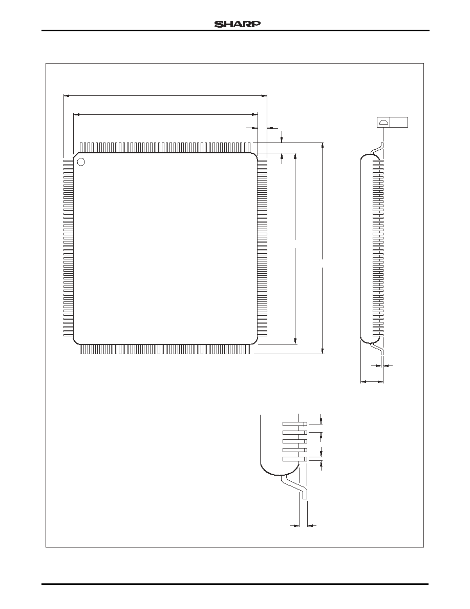
System-on-Chip
LH79520
Preliminary Data Sheet
9/10/03
45
PACKAGE SPECIFICATIONS
Figure 28. 176-pin LQFP
176LQFP-JEDEC
176LQFP (JEDEC MS-026)
1.00 REF.
1.00 REF.
0.40 (TYP.)
0.23
0.13
0.15
0.05
22.0 (TYP.)
20.0 (TYP.)
20.0 (TYP.)
22.0 (TYP.)
NOTES:
1. Dimensions in mm.
2. Refer to JEDEC MS-026 for tolerances.
DETAIL
1.40 NOM.
0.08
0.10
LH79520
System-on-Chip
46
9/10/03
Preliminary Data Sheet
Figure 29. Recommended PCB Footprint
21.25
17.2
1.67
17.2
19.58
0.25
22.92
0.4
79520-155
NOTE: Dimensions in mm.
System-on-Chip
LH79520
Preliminary Data Sheet
9/10/03
47
CONTENT REVISIONS
This document contains the following changes to
content, causing it to differ from previous versions.
Table 10. Record of Revisions
DATE
PAGE
NO.
PARAGRAPH OR
ILLUSTRATION
SUMMARY OF CHANGES
8-16-2002
1
Features
UART Data Rate changed to `Supports Data Rates up to 460.8 kb/s.
Synchronous Serial Port line added: Supports Data Rates up to 1.8452 Mb/s.
Line added: 5 V Tolerant Inputs.
22
DC Specifications
(Commercial)
VIH (MAX.) now 5.5 V
24
Table 6
Under `Synchronous Memory Interface Signals': D[31:0] Input parameter tISD
changed to 5 ns.
31
Table 9
Parameter tOSC expanded to include both the 14 MHz and the 32 kHz oscillators,
with the requisite (MAX.) timings.
34
Figure 23
Added a Shottky diode for fast risetime, plus an improved filter circuit
on VDDA.
7-30-2003
3
Figure 2
Revised `HR-TFT Timing Controller' to `Advanced LCD Interface'
14
Table 3
Corrected; added columns for 5:5:5+Intensity and 5:6:5 TFTs, Palette Data.
17
LCD Interface Con-
version Peripheral
(LCDICP)
Corrected to Advanced LCD Interface description, text updated for clarity.
22
DC Specifications
(Commercial)
Added `Typical' column, including values for IACTIVE, ISTANDBY, and ISLEEP.
26
DC Specifications
(Industrial)
Complete Industrial Specifications added.
23
AC Specifications
(Commercial)
Notation that PCLK is locked to HCLK in the LH79520.
31
Figure 11
Updated diagram.
32
Figures 12, 13, 14
Updated diagrams.
35
Figure 15
New figure to illustrate Synchronous Serial Port
38
Figures 19 and 20
Burst size added to captions.
39
Figures 21 and 22
New Figures to illustrate DMA Memory to Peripheral/Peripheral to Memory actions
41
Table 8, Figure 23
RESET release versus oscillator startup times clarified.
8-30-2003
43,44
Figures 26, 27
New Figures to illustrate Suggested External Components
13,
22, 26
DC Specifications
Input tolerance of clock inputs added.

LH79520
System-on-Chip
©2001 by SHARP Corporation
Reference Code SMA00067
SPECIFICATIONS ARE SUBJECT TO CHANGE WITHOUT NOTICE.
Suggested applications (if any) are for standard use; See Important Restrictions for limitations on special applications. See Limited
Warranty for SHARP's product warranty. The Limited Warranty is in lieu, and exclusive of, all other warranties, express or implied.
ALL EXPRESS AND IMPLIED WARRANTIES, INCLUDING THE WARRANTIES OF MERCHANTABILITY, FITNESS FOR USE AND
FITNESS FOR A PARTICULAR PURPOSE, ARE SPECIFICALLY EXCLUDED. In no event will SHARP be liable, or in any way responsible,
for any incidental or consequential economic or property damage.
NORTH AMERICA
EUROPE
JAPAN
SHARP Microelectronics of the Americas
5700 NW Pacific Rim Blvd.
Camas, WA 98607, U.S.A.
Phone: (1) 360-834-2500
Fax: (1) 360-834-8903
www.sharpsma.com
SHARP Microelectronics Europe
Division of Sharp Electronics (Europe) GmbH
Sonninstrasse 3
20097 Hamburg, Germany
Phone: (49) 40-2376-2286
Fax: (49) 40-2376-2232
www.sharpsme.com
SHARP Corporation
Electronic Components & Devices
22-22 Nagaike-cho, Abeno-Ku
Osaka 545-8522, Japan
Phone: (81) 6-6621-1221
Fax: (81) 6117-725300/6117-725301
www.sharp-world.com
TAIWAN
SINGAPORE
KOREA
SHARP Electronic Components
(Taiwan) Corporation
8F-A, No. 16, Sec. 4, Nanking E. Rd.
Taipei, Taiwan, Republic of China
Phone: (886) 2-2577-7341
Fax: (886) 2-2577-7326/2-2577-7328
SHARP Electronics (Singapore) PTE., Ltd.
438A, Alexandra Road, #05-01/02
Alexandra Technopark,
Singapore 119967
Phone: (65) 271-3566
Fax: (65) 271-3855
SHARP Electronic Components
(Korea) Corporation
RM 501 Geosung B/D, 541
Dohwa-dong, Mapo-ku
Seoul 121-701, Korea
Phone: (82) 2-711-5813 ~ 8
Fax: (82) 2-711-5819
CHINA
HONG KONG
SHARP Microelectronics of China
(Shanghai) Co., Ltd.
28 Xin Jin Qiao Road King Tower 16F
Pudong Shanghai, 201206 P.R. China
Phone: (86) 21-5854-7710/21-5834-6056
Fax: (86) 21-5854-4340/21-5834-6057
Head Office:
No. 360, Bashen Road,
Xin Development Bldg. 22
Waigaoqiao Free Trade Zone Shanghai
200131 P.R. China
Email: smc@china.global.sharp.co.jp
SHARP-ROXY (Hong Kong) Ltd.
3rd Business Division,
17/F, Admiralty Centre, Tower 1
18 Harcourt Road, Hong Kong
Phone: (852) 28229311
Fax: (852) 28660779
www.sharp.com.hk
Shenzhen Representative Office:
Room 13B1, Tower C,
Electronics Science & Technology Building
Shen Nan Zhong Road
Shenzhen, P.R. China
Phone: (86) 755-3273731
Fax: (86) 755-3273735