Document Outline
- ˛ˇ
- ˛ˇ
- ˛ˇ
- ˛ˇ
- ˛ˇ
- ˛ˇ
- ˛ˇ
- ˛ˇ
- ˛ˇ
- ˛ˇ
- ˛ˇ
- ˛ˇ
- ˛ˇ
- ˛ˇ
- ˛ˇ

LQ104V1DG51
TFT-LCD Module
(Model Number: LQ104V1DG51)
Specifications
Spec No.: LD-13708A
Dated: June , 2002
PREPARED BY : DATE
APPROVED BY : DATE
TFT Liquid Crystal Display Group
SHARP CORPORATION
SPECIFICATION
SPEC No. LD-13708A
FILE No.
ISSUE : Jul.18 2001
PAGE : 18 pages
APPLICABLE GROUP
TFT Liquid Crystal Display
Group
DEVICE SPECIFICATION FOR
TFT-LCD Module
MODEL No.
LQ104V1DG51
CUSTOMER'S APPROVAL
DATE
PRESENTED
BY
BY
K.Shiono
GeneralManager
Development Engineering Dept.
TFT Division.
TFT LIQUID CRYSTAL DISPLAY GROUP
SHARP CORPORATION

LD13708-1
1. Application
This technical literature applies to color TFT-LCD module, LQ104V1DG51
These technical literature sheets are the proprietary product of SHARP CORPORATION("SHARP) and
include materials protected under copyright of SHARP. Do not reproduce or cause any third party to
reproduce them in any form or by any means, electronic or mechanical, for any purpose, in whole or in part,
without the express written permission of SHARP .
The device listed in these technical literature sheets was designed and manufactured for use in general
electronic equipment.
In case of using the device for applications such as control and safety equipment for transportation(aircraft,
trains, automobiles, etc. ), rescue and security equipment and various safety related equipment which
require higher reliability and safety, take into consideration that appropriate measures such as fail-safe
functions and redundant system design should be taken .
Do not use the device for equipment that requires an extreme level of reliability, such as aerospace
applications, telecommunication equipment(trunk lines), nuclear power control equipment and medical or
other equipment for life support .
SHARP assumes no responsibility for any damage resulting from the use of the device which does not
comply with the instructions and the precautions specified in these technical literature sheets .
Contact and consult with a SHARP sales representative for any questions about this device .
2. Overview
This module is a color active matrix LCD module incorporating amorphous silicon TFT
(Thin Film Transistor). It is composed of a color TFT-LCD panel, driver ICs, control
circuit and power supply circuit and a backlight unit. Graphics and texts can be
displayed on a 640◊3◊480 dots panel with 262,144 colors by supplying 18 bit data signal
(6bit/color), four timing signals,+3.3V/ +5V DC supply voltage for TFT-LCD panel driving and
supply voltage for backlight.
The TFT-LCD panel used for this module is a low-reflection and higher-color-saturation
type. Therefore, this module is also suitable for the multimedia use.
Optimum viewing direction is 6 o'clock.
Backlight-driving DC/AC inverter is not built in this module.
LD13708-2
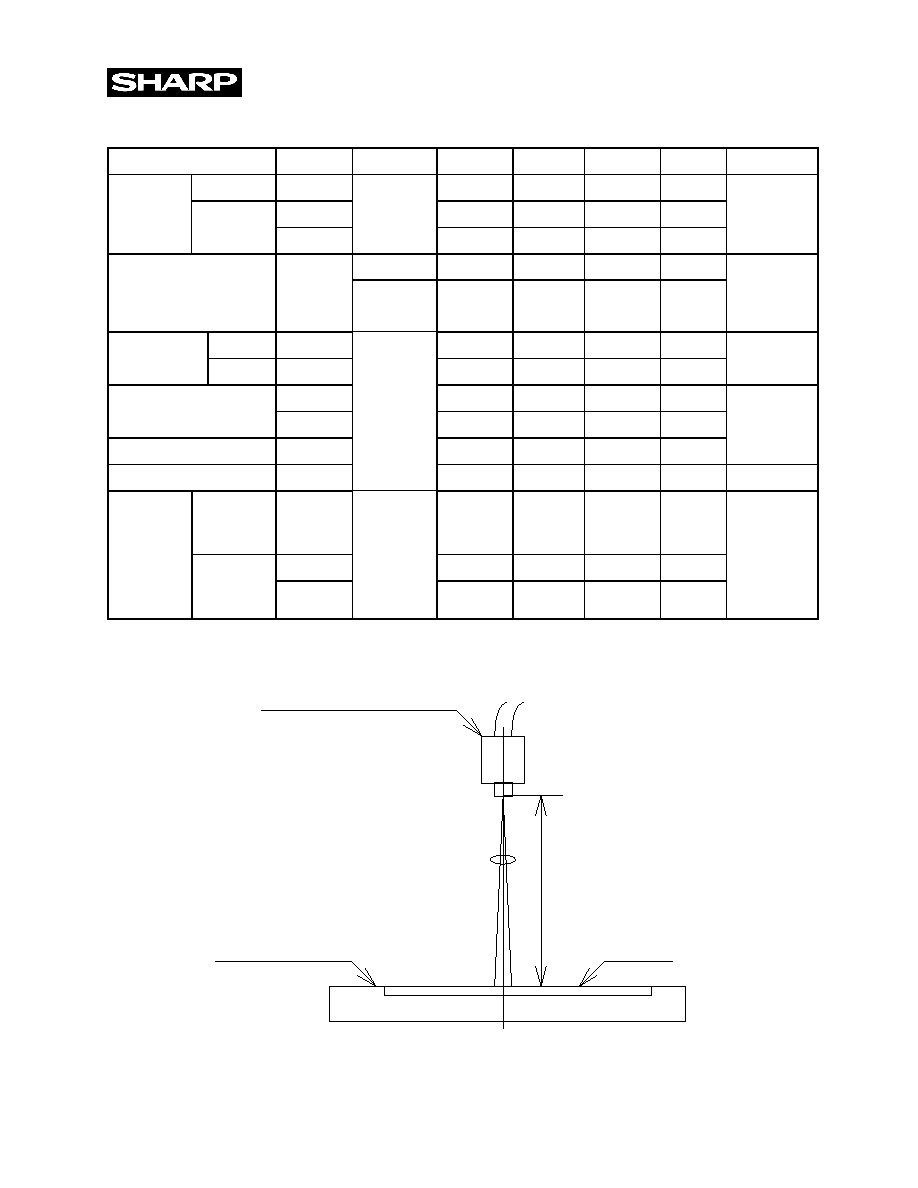
3. Mechanical Specifications
Parameter
Specifications
Unit
Display size
26 (10.4") Diagonal
cm
Active area
211.2(H)◊158.4(V)
mm
Pixel format
640(H)◊480(V)
pixel
(1 pixelRGB dots)
Pixel pitch
0.330(H)◊0.330(V)
mm
Pixel configuration
R,G,B vertical stripe
Display mode
Normally white
Unit outline dimensions *1
246.5(W)◊179.4(H)◊14.2(D)
mm
Mass
600±20
g
Surface treatment
Anti-glare and hard-coating
Haze value = 26%±5%
*1.Note: excluding backlight cables.
Outline dimensions is shown in Fig.1-1/Fig.1-2
LD13708-3
4. Input Terminals
4-1. TFT-LCD panel driving
CN1 Used connector:DF9MA-31P-1V (Hirose Electric Co., Ltd.)
Corresponding connector: DF9-31S-1V ( )
DF9A-31S-1V( )
DF9B-31S-1V( )
DF9M-31S-1V( )
Pin No.
Symbol
Function
Remark
1
GND
2
CK
Clock signal for sampling each data signal
3
Hsync Horizontal synchronous signal
Note1
4
Vsync Vertical synchronous signal
Note1
5
GND
6
R0
data signal(LSB
7
R1
data signal
8
R2
data signal
9
R3
data signal
10
R4
data signal
11
R5
data signal(MSB)
12
GND
13
G0
data signal(LSB
14
G1
data signal
15
G2
data signal
16
G3
data signal
17
G4
data signal
18
G5
data signal(MSB)
19
GND
20
B0
data signal(LSB
21
B1
data signal
22
B2
data signal
23
B3
data signal
24
B4
data signal
25
B5
data signal(MSB)
26
GND
27
ENAB Signal to settle the horizontal display position
Note2
28
Vcc
5.0V power supply
29
Vcc
5.0V power supply
30
R/L
Horizontal display mode select signal
Note3
31
U/D
Vertical display mode select signal
Note4
The shielding case is not connected with GND.
Note1480 line, 400 line or 350 line mode
is selected by the polarity combination
of the both synchronous signals.
Note2The horizontal display start timing is settled in
accordance with a rising timing of ENAB signal. In case ENAB is fixed "Low", the horizontal start timing is
determined as described in 7-2. Don't keep ENAB "High" during operation.
1
2
30
31
CN1 pin arrangement from module surface
(Transparent view)
Mode
480 lines
400 lines
350 lines
Hsync
negative
negative
Positive
Vsync
negative
positive
Negative
LD13708-4
Note3
Note4
4-2. Backlight driving
Used connector : BHR-03VS-1(JST)
CN2CN3 Corresponding connector :SM02(8.0)B-BHS(JST)
Pin no.
Symbol
Function
Cablecolor
1
HIGH
Power supply for lamp
(High voltage side)
Pink
2
NC
This is electrically opened.
3
LOW
Power supply for lamp
(Low voltage side)
White
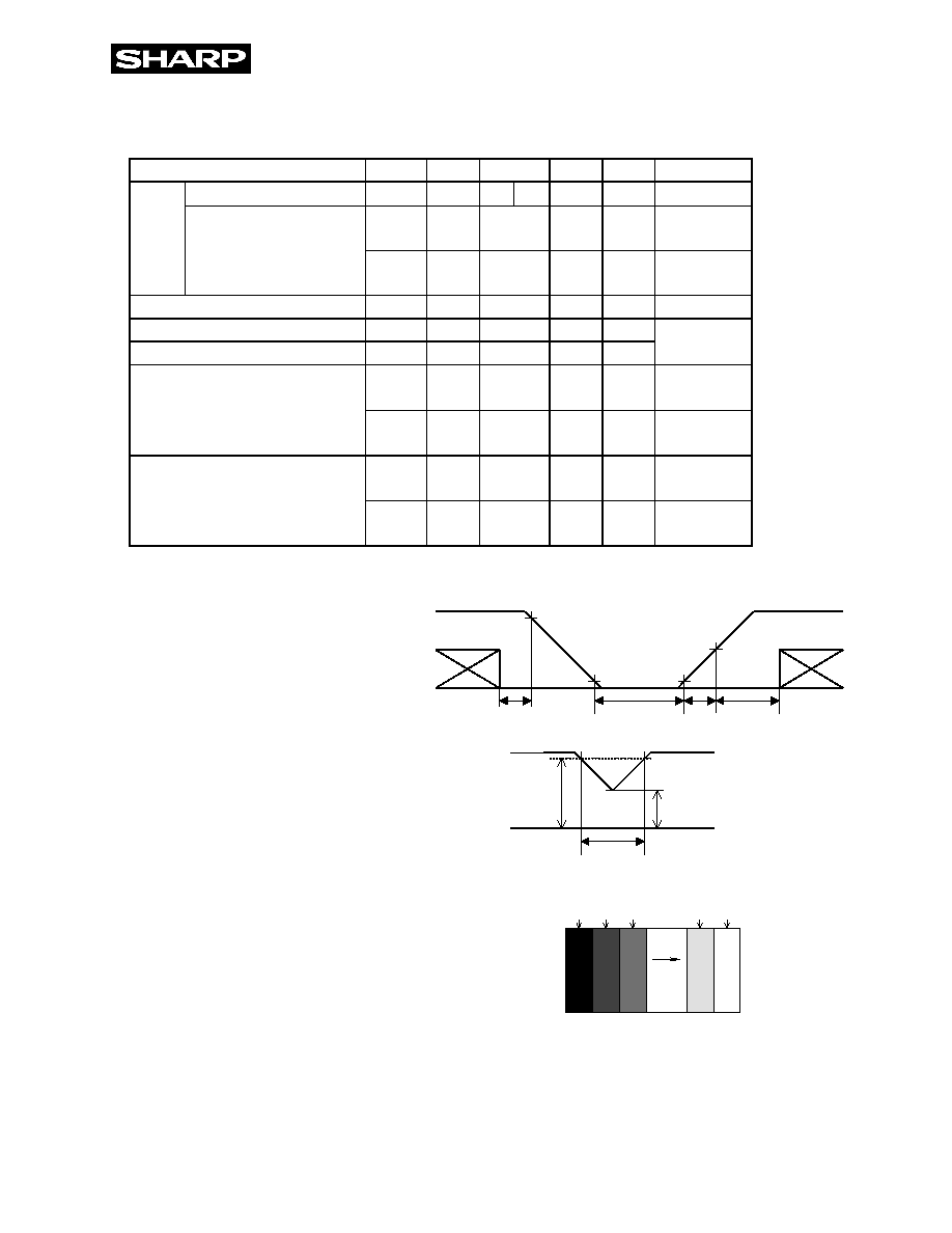
5. Absolute Maximum Ratings
Parameter
Symbol Condition
Ratings
Unit
Remark
Input voltage
V
I
Ta=25 0.3 Vcc0.3 Note1
+5V supply voltage
Vcc
Ta=25 0 6
Storage temperature
Tstg
30 70
Note2
Operating temperature (Ambient)
Topa
10 65
Note1CK,R0R5,G0G5,B0B5,Hsync,Vsync,ENAB, R/L, U/L
Note2Humidity95%RH Max. at Ta40.
Maximum wet-bulb temperature at 39 or less at Ta>40.
No condensation.
LD13708-5
6. Electrical Characteristics
6-1.TFT-LCDpaneldriving
Ta25
Parameter
Symbol
Min.
Typ.
Max.
Unit
Remark
Supply voltage
Vcc
+3.0 +3.3 +5.0
+5.5
V
Note1
Icc
350
400
Vcc=3.3V
Note2
Power
Supply Current dissipation
Icc
250
300
Vcc=5.0V
Note2
Permissive input ripple voltage
V
RF
100
mVp-p Vcc=+5V
Input voltage (Low)
V
IL
0.3Vcc
Input voltage (High)
V
IH
0.7Vcc
Note3
I
OL1
1.0
V
I
=0V
Note4
Input current (low)
I
OL2
60.0
V
I
=0V
Note5
Input current (High)
I
OH1
1.0
V
I
=Vcc
Note6
I
OH2
60.0
V
I
=Vcc
Note7
NOTE 1
Vcc-turn-on conditions
Vcc-dip conditions
Vcc-dip condition should also follow
The Vcc-turn-on conditions
Note2 Typical current situation : 16-gray-bar pattern.
480 line mode/Vcc=+3.3V/5.0V
Note3 CK,R0~R5,G0~G5,B0~B5,Hsync,Vsync,ENAB,
R/L,U/D
Note4 CK,R0~R5,G0~G5,B0~B5,Hsync,Vsync,ENAB
Note5 R/L
Note6 CK,R0~R5,G0~G5,B0~B5,Hsnc,Vsync
Note7 ENAB,U/D
T
4.5V
0.3V
VCC
T1
T
2.8V
0.3V
VCC
T
3.0V
2.7V
VCC
RGB
GS0
RGB
GS3
RGB
GS7
RGB
GS59
RGB
GS63
....
LD13708-6
6-2. Backlight driving
The backlight system is an edge-lighting type with single CCFT (Cold Cathode
Fluorescent Tube). The characteristics of single lamp are shown in the following table.
Ta=25
Parameter
Symbol
Min.
Typ.
Max.
Unit
Remark
Lamp current
I
L
3.5
6.0
7.0
mArms Note1
Lamp power consumption
P
L
2.8
Note2
Lamp frequency
F
L
40
60
70
KHz Note3
Kick-off voltage
Vs
1000
Vrms Ta=25
1300
Vrms Ta =0Note4
L
L
50000
hour Note5I
L
=6.0mA
Lamp life time
L
L
30000
hour Note5I
L=
7.0mA
Note1 Lamp current is measured with current meter for high frequency as shown below.
Note2 At the condition of Y
L
=350cd/m2
Note3 Lamp frequency may produce interference with horizontal synchronous frequency,and
this may cause beat on the display. Therefore lamp frequency shall be detached as
much as possible from the horizontal synchronous frequency and from the harmonics
of horizontal synchronous to avoid interference.
Note4The open output voltage of the inverter shall be maintained for more than 1sec; otherwise
the lamp may not be turned on.
Note5Since lamp is consumables, the life time written above is referencial value and it is not
guaranteed in this specification sheet by SHARP.
Lamp life time is defined that it applied either or under this condition
(Continuous turning on at Ta=25, IL=6/7mArms)
Brightness becomes 50% of the original value under standard condition.
Kick-off voltage at Ta=0 exceeds maximum value,(TBD) Vrms.
In case of operating under lower temp environment, the lamp exhaustion is accelerated and the
brightness becomes lower.
(Continuous operating under for around 1 month under lower temp condition may reduce the
brightness to half of the original brightness.)
In case of such usage under lower temp environment, periodical lamp exchange is recommended.
Note6The performance of the backlight, for example life time or brightness, is much influenced
by the characteristics of the DC-AC inverter for the lamp. When you design or order the
inverter, please make sure that a poor lighting caused by the mismatch of the backlight and
the inverter (miss-lighting,flicker, etc.) never occur. when you confirm it, the module should
be operated in the same condition as it is installed in your instrument.
Note7 It is required to have the inverter designed so that to allow the impedance deviation
of the two CCFT lamps and the capacity deviation of barast capacitor.
Module
Inverter
* 3pin is V
LOW
3
3
LD13708-7
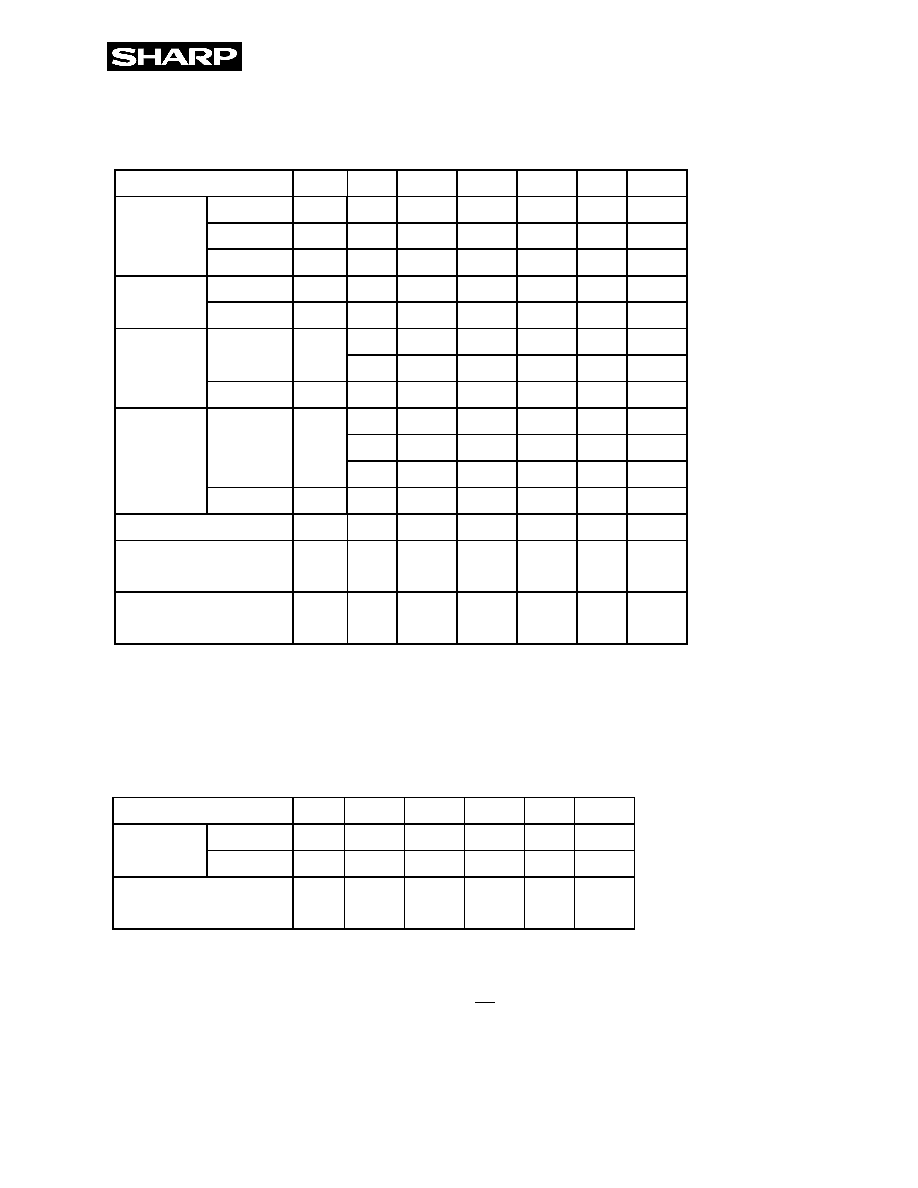
7. Timing Characteristics of input signals
Timing diagrams of input signal are shown in Fig.2 - .
7-1. Timing characteristics
Parameter
Symbol Mode
Min.
Typ.
Max.
Unit
Remark
Clock
Frequency
1/Tc
all
25.18
28.33
MHz
High time
Tch
5
ns
Low time
Tcl
10
ns
Data
Setup time
Tds
5
ns
Hold time
Tdh
10
ns
Horizontal
Cycle
TH
30.00
31.78
s
sync. signal
770
800
900
clock
Pulse width
THp
2
96
200
clock
Vertical
Cycle
TV
480
515
525
560
line
sync. signal
400
445
449
480
line
350
447
449
510
line
Pulsewidth
TVp
all
1
34
line
Horizontal display period
THd
640
640
640
clock
Hsync-Clock
THc
10
Tc-10
ns
phase difference
Hsync-Vsync
TVh
0
TH-THp clock
phase difference
Note) In case of lower frequency, the deterioration of display quality, flicker etc.,may be occurred.
7-2. Horizontal display position
The horizontal display position is determined by ENAB signal and the input data corresponding
to the rising edge of ENAB signal is displayed at the left end of the active area.
Parameter
symbol
Min.
Typ.
Max.
Unit
Remark
Enable signal Setup time
Tes
5
Tc-10
ns
Pulse width
Tep
2
640
640
clock
Hsync-Enable signal
phase difference
THe
44
TH-664 clock
Note) When ENAB is fixed "Low", the display starts from the data of C104(clock) as shown
in Fig.2-. Be careful that the module does not work when ENAB is fixed "High".
When the phase difference is below 104 clock, keep the "High level of ENAB is signal longer
Than 104-The. If it will not be keeped, the display starts from the data of C104(clock).
LD13708-8
7-3. Vertical display position
The vertical display position is automatically centered in the active area at each mode
of VGA ,480-,400-,and 350-line mode . Each mode is selected depending on the polarity of
the synchronous signals described in 4-1(Note1).
In each mode ,the data of TVn is displayed at the top line of the active area. And the
display position will be centered on the screen like the following figure when the period of
vertical synchronous signal,TV,is typical value.
In 400-,and 350-line mode,the data in the vertical data invalid period is also displayed,
So ,inputting all data "0" is recommended during vertical data invalid period.
ENAB signal has no relation to the vertical display position.
Mode V-data start(TVs)
V-data
period(TVd)
V-display start(TVn) V-display period Unit
Remark
480
34
480
34
480
line
400
34
400
443-TV
480
line
350
61
350
445-TV
480
line
7-4. Input Data Signals and Display Position on the screen
data invalid period
lines
lines
lines
lines
lines
lines
400 lines mode (TV=449)
350 lines mode (TV=449)
data period
data invalid period
data invalid period
data invalid period
data period
D1,DH1
D1,DH2
D1,DH3
D2,DH2
D2,DH1
D3,DH1
D640,DH1
D640,DH480
D1,DH480
R
G
B
Display position of input data (480 lines mode)
THc
C1*
C2*
* Only when enable terminal is fixed "Low"
D1
D2
D3
Tds Tdh
Tch Tcl
Tc
D639
D640
Horizontal invalid da ta period
THp
C104*
Number of clock
Number of H-data
THe
Tes
THd
Tep
TH
DH1
DH2
DH3
DH479
DH480
Vertical invalid data period
TVh
TVp
TV
TVs
TVd
Number of V-data line
1
2
34
Fig 2-1 Input signal waveforms (480 line m
Horizontal
sync. signal
(Hsync)
Clock signal
(CK)
Data signal
(R0~R5,G0~G5,
B0~B5)
Data enable signal
(ENAB)
Vertical
sync. signal
(Vsync)
Horizontal
sync.
signal
(Hsync)
Data signal
(R0~R5,G0~G5,
B0~B5)
Horizontal invalid da ta period
Vertical invalid data period
0 . 3 V c c
0 . 3 V c c
0 . 3 V c c
0 . 3 V c c
0 . 7 V c c
0 . 3 V c c
0 . 3 V c c
0 . 7 V c c
0 . 3 V c c
0 . 7 V c c
0 . 3 V c c
0 . 3 V c c
0 . 3 V c c
0 . 7 V c c
0 . 7 V c c
0 . 3 V c c
0 . 3 V c c
0 . 7 V c c
N u m b e r o f l i n e
Fig2-1Inputsignalwaveforms(480linemode)
THc
C1*
C2*
* Only when enable terminal (ENAB) is fixed
D1
D2
D3
Tds Tdh
Tch Tcl
Tc
D639 D640
Horizontal data invalid
period
THp
C104*
Number of H-data
THe
Tes
THd
Tep
TH
DH1
DH2
DH3
DH399 DH400
Vertical invalid data period
TVh
TVp
TV
TVs
TVd
1
2
34
Number of line
Fig.2-2 Input signal waveforms (400 line
Horizontal
sync.
signal
(Hsync)
Clock signal
(CK)
Data signal
(R0~R5,G0~G5,
B0~B5)
Data enable
signal
(ENAB)
Vertical
sync.
signal
(Vsync)
Horizontal
sync. signal
(Hsync)
Data signal
(R0~R5,G0~G5,
B0~B5)
Horizontal data invalid
period
Vertical invalid data period
0 . 3 V c c
0 . 3 V c c
0 . 3 V c c
0 . 7 V c c
0 . 7 V c c
0 . 3 V c c
0 . 3 V c c
0 . 3 V c c
0 . 7 V c c
0 . 3 V c c
0 . 3 V c c
0 . 3 V c c
0 . 7 V c c
0 . 3 V c c
0 . 7 V c c
0 . 7 V c c
0 . 7 V c c
N u m b e r o f c l o c k
N u m b e r o f V - d a t a l i n e
Fig2-2Inputsignalwaveforms(400linemode)
Horizontal
sync. signal
(Hsync)
Clock signal
(CK)
Data signal
(R0~R5,G0~G5,
B0~B5)
THc
C1*
C2*
D1
D2
D3
Tds Tdh
Tch Tcl
Tc
D639
D640
Horizontal invalid data period
Data enable signal
(ENAB)
C104*
Number of H-data
THe
Tes
THd
Tep
THp
TH
DH1
DH2
DH3
DH349
DH350
Vertical invalid data period
Vertical
sync. signal
(Vsync)
TVh
TVp
TV
TVs
TVd
Number of V-data line
1
2
Number of
li
Fig.2-3 Input signal waveforms (350 line mod
61
Horizontal
sync. signal
(Hsync)
Data signal
(R0~R5,G0~G5,
B0~B5)
* Only when enable terminal (ENAB) fixed to "Low
Horizontal invalid data
period
Vertical invalid data period
0 . 7 V c c
0 . 7 V c c
0 . 7 V c c
0 . 3 V c c
0 . 3 V c c
0 . 3 V c c
0 . 3 V c c
0 . 7 V c c
0 . 3 V c c
0 . 7 V c c
0 . 3 V c c
0 . 3 V c c
0 . 7 V c c
0 . 3 V c c
0 . 7 V c c
0 . 3 V c c
0 . 3 V c c
N u m b e r o f c l o c k
1
1
1
1
Fig2-3Inputsignalwaveforms(350linemode)
LD13708-12
8. Input Signals, Basic Display Colors and Gray Scale of Each Color
Colors &
Data signal
Gray scale
Gray
RA0 RA1 RA2 RA3 RA4 RA5 GA0 GA1 GA2 GA3 GA4 GA5 BA0 BA1 BA2 BA3 BA4 BA5
Scale
RB0 RB1 RB2 RB3 RB4 RB5 GB0 GB1 GB2 GB3 GB4 GB5 BB0 BB1 BB2 BB3 BB4 BB5
Black
0
0
0
0
0
0
0
0
0
0
0
0
0
0
0
0
0
0
Blue
0
0
0
0
0
0
0
0
0
0
0
0
1
1
1
1
1
1
Green
0
0
0
0
0
0
1
1
1
1
1
1
0
0
0
0
0
0
Cyan
0
0
0
0
0
0
1
1
1
1
1
1
1
1
1
1
1
1
Red
1
1
1
1
1
1
0
0
0
0
0
0
0
0
0
0
0
0
Magenta
1
1
1
1
1
1
0
0
0
0
0
0
1
1
1
1
1
1
Yellow
1
1
1
1
1
1
1
1
1
1
1
1
0
0
0
0
0
0
White
1
1
1
1
1
1
1
1
1
1
1
1
1
1
1
1
1
1
Black
GS0
0
0
0
0
0
0
0
0
0
0
0
0
0
0
0
0
0
0
GS1
1
0
0
0
0
0
0
0
0
0
0
0
0
0
0
0
0
0
Darker
GS2
0
1
0
0
0
0
0
0
0
0
0
0
0
0
0
0
0
0
Brighter
GS61
1
0
1
1
1
1
0
0
0
0
0
0
0
0
0
0
0
0
GS62
0
1
1
1
1
1
0
0
0
0
0
0
0
0
0
0
0
0
Red
GS63
1
1
1
1
1
1
0
0
0
0
0
0
0
0
0
0
0
0
Black
GS0
0
0
0
0
0
0
0
0
0
0
0
0
0
0
0
0
0
0
GS1
0
0
0
0
0
0
1
0
0
0
0
0
0
0
0
0
0
0
Darker
GS2
0
0
0
0
0
0
0
1
0
0
0
0
0
0
0
0
0
0
Brighter
GS61
0
0
0
0
0
0
1
0
1
1
1
1
0
0
0
0
0
0
GS62
0
0
0
0
0
0
0
1
1
1
1
1
0
0
0
0
0
0
Green
GS63
0
0
0
0
0
0
1
1
1
1
1
1
0
0
0
0
0
0
Black
GS0
0
0
0
0
0
0
0
0
0
0
0
0
0
0
0
0
0
0
GS1
0
0
0
0
0
0
0
0
0
0
0
0
1
0
0
0
0
0
Darker
GS2
0
0
0
0
0
0
0
0
0
0
0
0
0
1
0
0
0
0
Brighter
GS61
0
0
0
0
0
0
0
0
0
0
0
0
1
0
1
1
1
1
GS62
0
0
0
0
0
0
0
0
0
0
0
0
0
1
1
1
1
1
Blue
GS63
0
0
0
0
0
0
0
0
0
0
0
0
1
1
1
1
1
1
0 :Low level voltage, 1 : High level voltage
Each basic color can be displayed in 64 gray scales from 6 bit data signals. According to the combination of total 18 bit
B
a
s
i
c
C
o
l
o
r
B
a
s
i
c
C
o
l
o
r
B
a
s
i
c
C
o
l
o
r
B
a
s
i
c
C
o
l
o
r
G
r
a
y
S
c
a
l
e
o
f
R
e
d
G
r
a
y
S
c
a
l
e
o
f
R
e
d
G
r
a
y
S
c
a
l
e
o
f
R
e
d
G
r
a
y
S
c
a
l
e
o
f
R
e
d
G
r
a
y
S
c
a
l
e
o
f
G
r
e
e
n
G
r
a
y
S
c
a
l
e
o
f
G
r
e
e
n
G
r
a
y
S
c
a
l
e
o
f
G
r
e
e
n
G
r
a
y
S
c
a
l
e
o
f
G
r
e
e
n
G
r
a
y
S
c
a
l
e
o
f
B
l
u
e
G
r
a
y
S
c
a
l
e
o
f
B
l
u
e
G
r
a
y
S
c
a
l
e
o
f
B
l
u
e
G
r
a
y
S
c
a
l
e
o
f
B
l
u
e
LD13708-13
data signals, the 262,144-color display can be achieved on the screen.
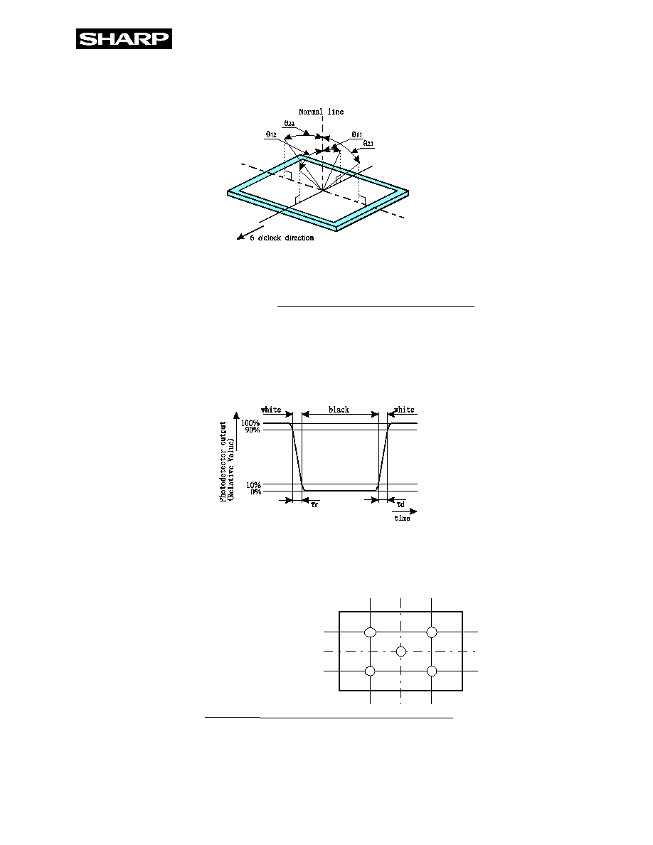
9. Optical Characteristics
Ta=25, Vcc=+5V
Parameter
Symbol
Condition
Min
Typ
Max
Unit
Remark
Viewing
Horizontal 21,22
60
70
Deg.
Note1,4
Angle
Vertical
11
35
40
Deg.
Range
12
55
70
Deg.
=∞
150
Contrast ratio
Best
Viewing
Angle
300
Note2,4
Response
Rise
r
=∞
20
Note
3,4
Time
Decay
d
40
Chromaticity of
0.313
Note4
White
0.329
Luminance of white
350
cd/m
2
White Unifomity
1.45
Note5
Horizontal 21,22
45
Deg.
11
35
Deg.
Viewing
Angle
range as a
Brightness
Definition
Vertical
12
50% of
the
maximum
brightness
35
Deg.
Note1
The measurement shall be executed 30 minutes after
li
ghting at
rating.
(typical condition:I
L
=
6.0mArms)
The optical characteristics shall be measured in a dark room or equivalent state
with the method shown in Fig.3 below.
Photodetector (BM-5A:TOPCON)
Fig.3 Optical characteristics measurement method
Center of the screen
module
∞
panel
LD13708-14
Note1Definitions of viewing angle range:
Note2Definition of contrast ratio:
The contrast ratio is defined as the following.
Contrast Ratio (CR)
Note3Definition of response time:
The response time is defined as the following figure and shall be measured by
switching the input signal for "black" and "white" .
Note4This shall be measured at center of the screen.
Note5Definition of white uniformity:
White uniformity is defined as the
following with five measurements
(AE).
Luminance (brightness) with all pixels white
Luminance (brightness) with all pixels black
A
B
C
D
E
160
320
480
120
240
360
pixel
pixel
Maximum Luminance of five points (brightness)
Minimum Luminance of five points (brightness)
w
LD13708-15
10. Display Quantity
The display quality of the color TFT-LCD module shall be in compliance with the
Incoming Inspection Standard.
11Handling Precautions
a) Be sure to turn off the power supply when inserting or disconnecting the cable.
b) Be sure to design the cabinet so that the module can be installed without any extra stress such as
warp or twist.
c) Since the front polarizer is easily damaged, pay attention not to scratch it.
d) Wipe off water drop immediately. Long contact with water may cause discoloration or spots.
e) When the panel surface is soiled, wipe it with absorbent cotton or other soft cloth.
f) Since the panel is made of glass, it may break or crack if dropped or bumped on hard surface.
Handle with care.
g) Since CMOS LSI is used in this module, take care of static electricity and injure the human earth
when handling.
h) Observe all other precautionary requirements in handling components.
i) This module has its circuitry PCBs on the rear side and should be carefully handled in order not
to be stressed.
j) The polarizer surface on the panel is treated with Anti-Glare for low reflection. In case of attaching
protective board over the LCD. Be careful about the optical interface fringe etc.
Which degrades display quality.
k) Connect GND to 4 place of mounting holes to stabilize against EMI and external noise.
l) There are high voltage portions on the backlight and very dangerous. Careless touch may lead to
electrical shock. When exchange lamps or service. Turn off the power without tail.
m) Be sure not to apply tensile stress to the lamp lead cable.
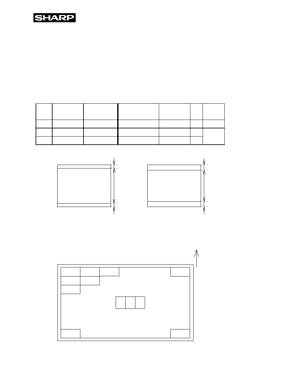
12.Packing form
Product country
JAPAN
Piling number of cartons
Max
Packing quantity in one carton
20
Carton size[mm]
494(W)
◊326(D)◊433(H)
Total mass of one carton filled
with full modules
15.6kg
Packing form is shown
Fig.1-2
LD13708-16
13Reliability test items
No. Test item
Conditions
1 High temperature storage test
Ta=70 240h
2 Low temperature storage test
Ta=-30 240h
3 High temperature
& high humidity operation test
Ta=40 ; 95%RH 240h
(No condensation)
4 High temperature operation test
Ta=65 240h
5 Low temperature operation test
Ta=-10 240h
6 Vibration test
(non- operating)
Frequency: 1057Hz/Vibration width (one side):0.075mm
: 58500Hz/Gravity:9.8m/s
2
Sweep time : 11 minutes
Test period : 3 hours
(1 hour for each direction of X,Y,Z)
7 Shock test
(non- operating)
Max. gravity : 490m/s
2
Pulse width : 11ms, half sine wave
Direction : ±X,±Y,±Z
once for each direction.
Result Evaluation Criteria
Under the display quality test conditions with normal operation state, these shall be no change
which may affect practical display function.
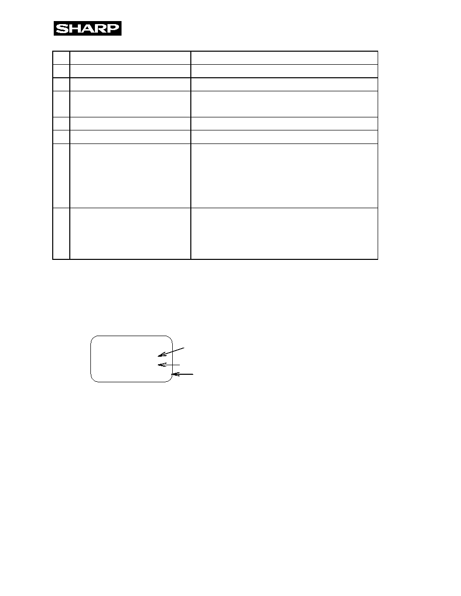
14Others
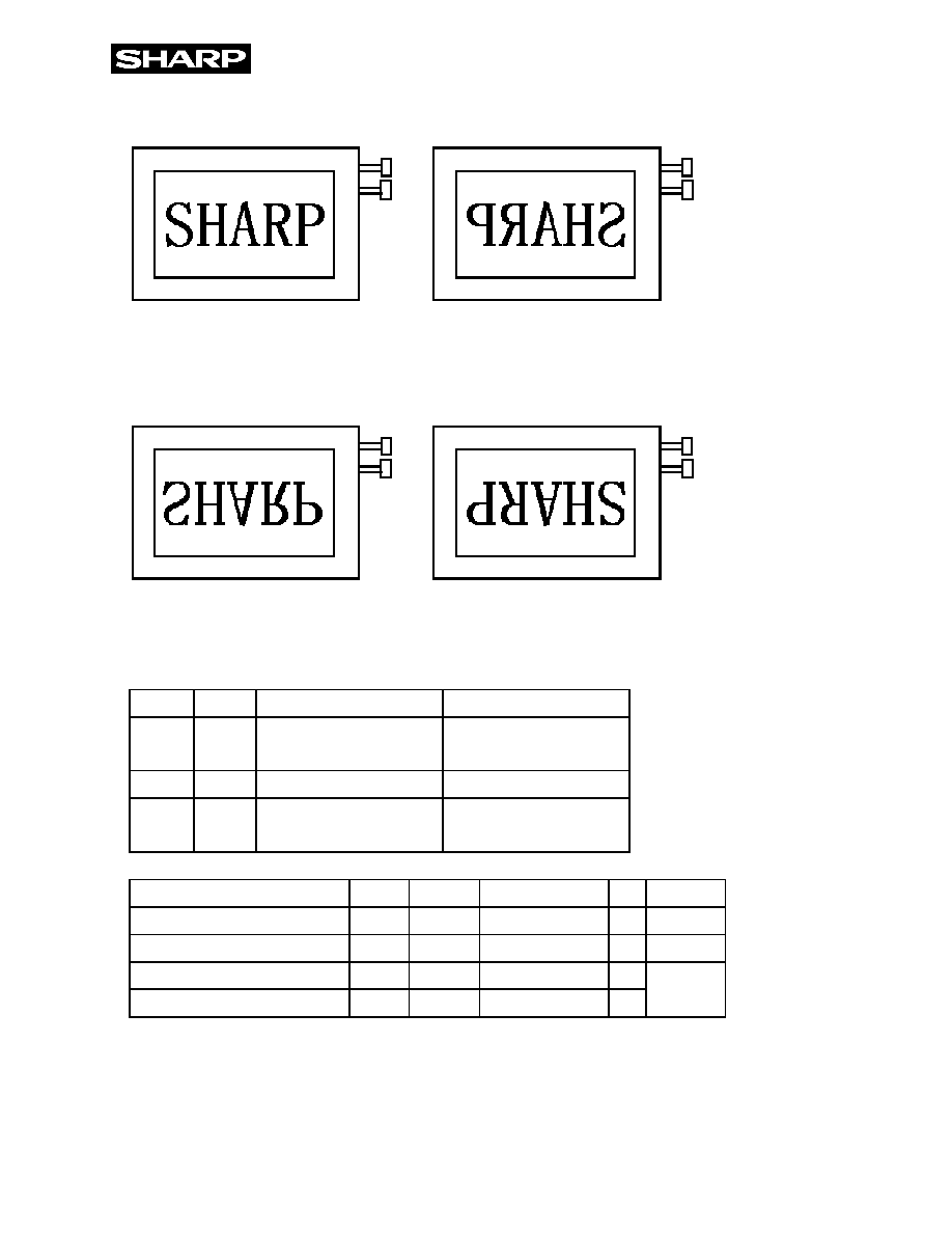
1) Lot No Label:
S H A R P
LQ104V1DG51
07 XXXXXX
MADE IN
Model No.
Lot No.
JAPAN
2) Adjusting volume have been set optimally before shipment, so do not change any adjusted value.
If adjusted value is changed, the specification may not be satisfied.
3) Disassembling the module can cause permanent damage and should be strictly avoided.
4) Please be careful since image retention may occur when a fixed pattern is displayed for a long
time
5) Do not use LCD module in the atmosphere of corrosive gases, such as sulfide gas or chlorine gases.
Polarizer may deteriorated or cause chemical reaction that can lead to short circuits at the terminal
Points. Do not use the material, which compounds contain sulfide or chlorine articles in the vicinity of
LCD module. At high temperature, these compounds produce corrosive gases.
6) If any problem occurs in relation to the description of this specification , it shall be resolved
through discussion with spirit of cooperation.

SPECIFICATIONS ARE SUBJECT TO CHANGE WITHOUT NOTICE.
Suggested applications (if any) are for standard use; See Important Restrictions for limitations on special applications. See Limited
Warranty for SHARP's product warranty. The Limited Warranty is in lieu, and exclusive of, all other warranties, express or implied.
ALL EXPRESS AND IMPLIED WARRANTIES, INCLUDING THE WARRANTIES OF MERCHANTABILITY, FITNESS FOR USE AND
FITNESS FOR A PARTICULAR PURPOSE, ARE SPECIFICALLY EXCLUDED. In no event will SHARP be liable, or in any way responsible,
for any incidental or consequential economic or property damage.
NORTH AMERICA
EUROPE
JAPAN
SHARP Microelectronics of the Americas
5700 NW Pacific Rim Blvd.
Camas, WA 98607, U.S.A.
Phone: (1) 360-834-2500
Fax: (1) 360-834-8903
Fast Info: (1) 800-833-9437
www.sharpsma.com
SHARP Microelectronics Europe
Division of Sharp Electronics (Europe) GmbH
Sonninstrasse 3
20097 Hamburg, Germany
Phone: (49) 40-2376-2286
Fax: (49) 40-2376-2232
www.sharpsme.com
SHARP Corporation
Electronic Components & Devices
22-22 Nagaike-cho, Abeno-Ku
Osaka 545-8522, Japan
Phone: (81) 6-6621-1221
Fax: (81) 6117-725300/6117-725301
www.sharp-world.com
TAIWAN
SINGAPORE
KOREA
SHARP Electronic Components
(Taiwan) Corporation
8F-A, No. 16, Sec. 4, Nanking E. Rd.
Taipei, Taiwan, Republic of China
Phone: (886) 2-2577-7341
Fax: (886) 2-2577-7326/2-2577-7328
SHARP Electronics (Singapore) PTE., Ltd.
438A, Alexandra Road, #05-01/02
Alexandra Technopark,
Singapore 119967
Phone: (65) 271-3566
Fax: (65) 271-3855
SHARP Electronic Components
(Korea) Corporation
RM 501 Geosung B/D, 541
Dohwa-dong, Mapo-ku
Seoul 121-701, Korea
Phone: (82) 2-711-5813 ~ 8
Fax: (82) 2-711-5819
CHINA
HONG KONG
SHARP Microelectronics of China
(Shanghai) Co., Ltd.
28 Xin Jin Qiao Road King Tower 16F
Pudong Shanghai, 201206 P.R. China
Phone: (86) 21-5854-7710/21-5834-6056
Fax: (86) 21-5854-4340/21-5834-6057
Head Office:
No. 360, Bashen Road,
Xin Development Bldg. 22
Waigaoqiao Free Trade Zone Shanghai
200131 P.R. China
Email: smc@china.global.sharp.co.jp
SHARP-ROXY (Hong Kong) Ltd.
3rd Business Division,
17/F, Admiralty Centre, Tower 1
18 Harcourt Road, Hong Kong
Phone: (852) 28229311
Fax: (852) 28660779
www.sharp.com.hk
Shenzhen Representative Office:
Room 13B1, Tower C,
Electronics Science & Technology Building
Shen Nan Zhong Road
Shenzhen, P.R. China
Phone: (86) 755-3273731
Fax: (86) 755-3273735