 | –≠–ª–µ–∫—Ç—Ä–æ–Ω–Ω—ã–π –∫–æ–º–ø–æ–Ω–µ–Ω—Ç: PC3H7BC | –°–∫–∞—á–∞—Ç—å:  PDF PDF  ZIP ZIP |
PC3H7/PC3Q67Q
PC3H7/PC3Q67Q
s
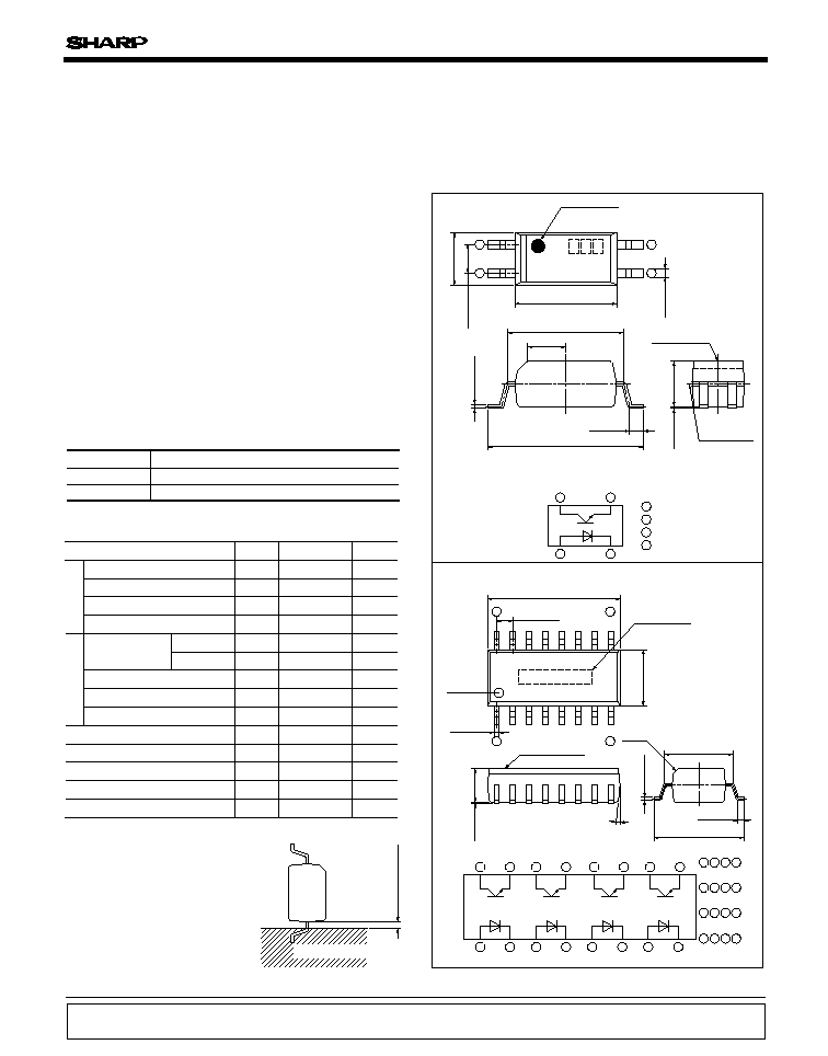
Package Specifications
s
Outline Dimensions
(Unit : mm)
Mini-falt Package, General
Purpose Half Pitch
Photocoupler
1. Programmable controllers
s
Features
s
Applications
1. Mini-flat package
2. Half pitch type (lead pitch : 1.27mm)
3. Isolation voltage (Viso : 2 500Vrms)
4. Applicable to infrared ray reflow (230∞C, for MAX. 30s)
5. High reliability
6. Taping package
PC3H7
(1ch)
PC3Q67Q
(4ch)
7. Recognized by UL, file No. E64380
Approved by VDE, No.5922UG
Model No.
PC3H7
PC3Q67Q
Taping specifications
Taping reel diameter 330mm (3 000pcs.)
Taping reel diameter 330mm (1 000pcs.)
s
Absolute Maximum Ratings
Parameter
Rating
Input
Output
Collector-emitter
voltage
PC3H7
PC3Q67Q
Emitter-collector voltage
Collector current
Operating temperature
Symbol
I
F
I
FM
P
V
CEO
V
CEO
V
ECO
I
C
P
C
P
tot
V
iso
T
opr
T
stg
T
sol
50
1
70
70
6
50
150
170
2.5
-
30 to
+
100
-
40 to
+
125
260
*1 Pulse width
<=
100
µ
s, Duty ratio : 0.001
*2 AC for 1min, 40 to 60%RH, f
=
60Hz
*3 For 10s
Forward current
Power dissipation
Collector power dissipation
Total power dissipation
Storage temperature
*3
Soldering temperature
*2
Isolation voltage
*1
Peak forward current
Unit
mA
A
mW
V
R
6
Reverse voltage
V
V
35
V
V
mA
mW
mW
∞C
∞C
∞C
kV
rms
(Ta
=
25∞C)
S
3 H 7
1
2
4
3
4
2
1
3
4.4
±
0.2
5.3
±
0.3
0.2
±
0.05
7.0
+
0.2
-
0.7
(1.7)
1.27
±
0.25
2.6
±
0.3
0.4
±
0.1
0.5
+
0.4
-
0.2
2.0
±
0.2
0.1
±
0.1
1
2
3
4
Anode
Cathode
Emitter
Collector
Internal connection diagram
g
( ) : Reference dimensions
Anode mark
Epoxy resin
Parting line
Model No.
C0.4
Epoxy resin
6
∞
Primary
Side
mark
10.3
±
0.3
1.27
±
0.25
4.4
±
0.2
16
1
8
9
0.5
+
0.4
-
0.2
7.0
+
0.2
-
0.7
0.4
±
0.1
2.6
±
0.2
0.1
±
0.1
0.2
±
0.05
5.3
±
0.3
Internal connection diagram
Anode
Cathode
Emitter
Collector
1
2
3
4
5
6
7
8
2 4 6 8
10 12 14 16
9 11 13 15
1 3 5 7
16
15
14
13
12
11
10
9
0.2mm or more
Soldering area
Notice
In the absence of confirmation by device specification sheets, SHARP takes no responsibility for any defects that may occur in equipment using any SHARP
devices shown in catalogs, data books, etc. Contact SHARP in order to obtain the latest device specification sheets before using any SHARP device.
Internet
Internet address for Electronic Components Group http://www.sharp.co.jp/ecg/
PC3H7
PC3Q67Q
PC3H7/PC3Q67Q
s
Electro-optical Characteristics
Parameter
Conditions
Input
Forward voltage
I
F
=
20mA
Terminal capacitance
Output
V
CE
=
50V, I
F
=
0
Collector-emitter
I
C
=
0.1mA, I
F
=
0
Emitter-collector
I
E
=
10
µ
A, I
F
=
0
Transfer
charac-
teristics
Collector current
I
F
=
1mA, V
CE
=
5V
Collector-emitter
saturation voltage
I
F
=
20mA
I
C
=
1mA
Isolation resistance
DC500V
40 to 60%RH
Floating capacitance
V
=
0, f
=
1MHz
Response time
Rise time
Fall time
PC3H7
PC3Q67Q
PC3H7
PC3Q67Q
PC3H7
PC3Q67Q
MIN.
-
-
-
70
6
0.2
-
5
◊
10
10
-
-
-
TYP.
1.2
30
-
-
-
0.1
1
◊
10
11
0.6
4
3
MAX.
1.4
250
100
-
-
35
-
-
-
4
0.2
-
1.0
18
18
Collector dark current
breakdown voltage
breakdown voltage
Symbol
V
F
C
t
I
CEO
BV
CEO
I
C
=
0.1mA, I
F
=
0
BV
CEO
BV
ECO
I
C
I
F
=
5mA, V
CE
=
5V
I
C
V
CE(sat)
C
f
t
r
t
f
R
ISO
V
=
0, f
=
1kHz
Unit
V
Reverse current
V
R
=4V
-
-
10
I
R
µ
A
nA
V
CE
=
20V, I
F
=
0
-
-
100
I
CEO
nA
V
V
V
mA
2.5
5
30
mA
V
pF
pF
µ
s
µ
s
V
CE
=
2V
I
C
=
2mA
R
L
=
100
(Ta
=
25∞C)
F
o
r
w
a
r
d
c
u
r
r
e
n
t
I
F
(
m
A
)
0
10
20
30
40
50
60
-
30
0
25
75
100
125
55
50
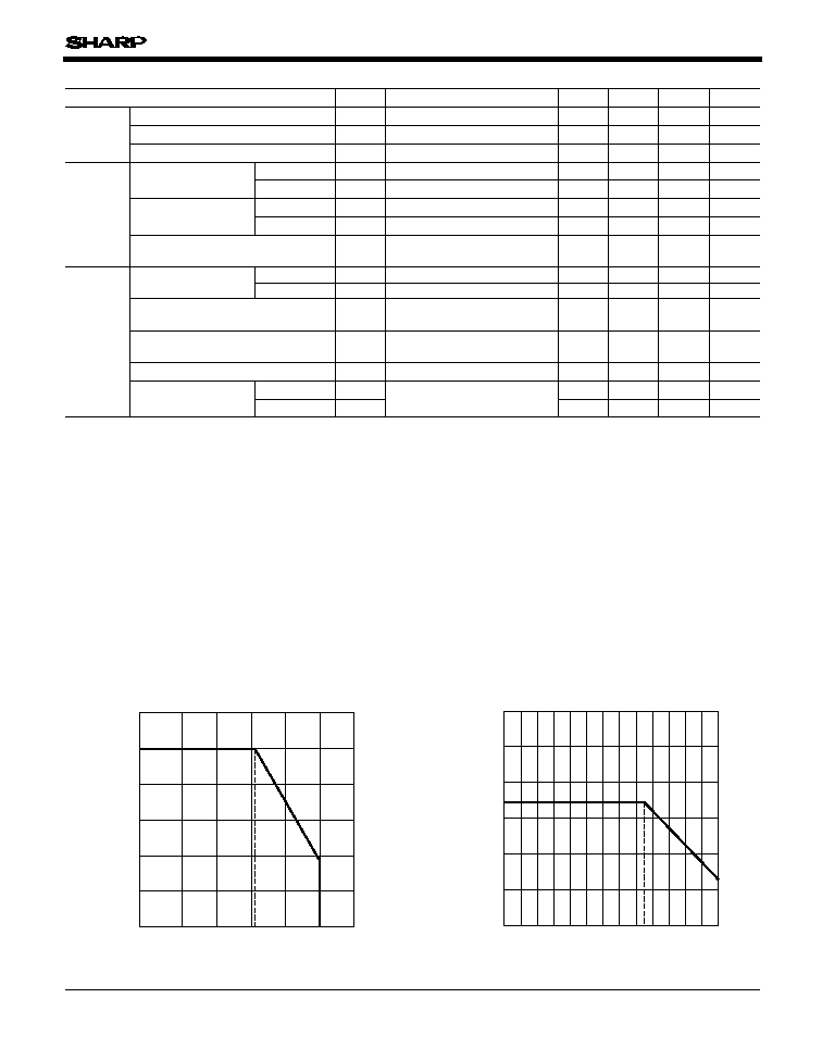
Ambient temperature T
a
(
∞
C)
D
i
o
d
e
p
o
w
e
r
d
i
s
s
i
p
a
t
i
o
n
P
(
m
W
)
0
100
80
60
70
40
20
-
30
0
55
100
50
Ambient temperature T
a
(
∞
C)
Fig.1 Forward Current vs. Ambient
Temperature
Fig.2 Diode Power Dissipation vs. Ambient
Temperature
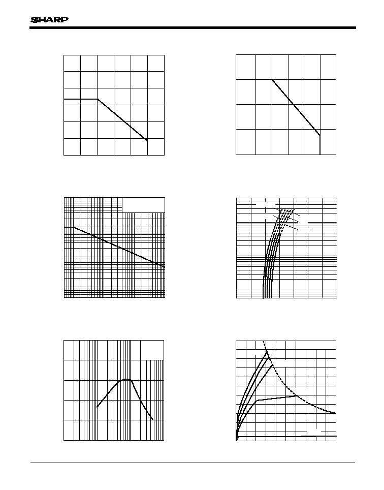
PC3H7/PC3Q67Q
P
o
w
e
r
d
i
s
s
i
p
a
t
i
o
n
P
t
o
t
(
m
W
)
0
250
200
150
170
100
50
-
30
0
25
50
75
100
Ambient temperature T
a
(
∞
C)
Forward voltage V
F
(V)
50
∞C
25
∞C
0
∞C
0
2
0.5
1.0
1.5
2.0
2.5
3.0
3.5
5
10
20
50
100
200
500
1
-
25
∞C
Ta
=
75∞C
F
o
r
w
a
r
d
c
u
r
r
e
n
t
I
F
(
m
A
)
C
o
l
l
e
c
t
o
r
p
o
w
e
r
d
i
s
s
i
p
a
t
i
o
n
P
C
(
m
W
)
0
200
150
100
50
-
30
0
25
50
75
100
125
Ambient temperature T
a
(
∞
C)
Pulse width
<=
100
µ
s
T
a
=
25
∞
C
P
e
a
k
f
o
r
w
a
r
d
c
u
r
r
e
n
t
I
F
M
(
m
A
)
5
10000
5000
2000
1000
500
200
100
50
20
10
5
2
10
-
3
5
2
10
-
2
5
2
10
-
1
5
1
Duty ratio
C
u
r
r
e
n
t
t
r
a
n
s
f
e
r
r
a
t
i
o
C
T
R
(
%
)
0
500
400
300
200
100
0.1
1
10
100
Forward current I
F
(mA)
V
CE
=
5V
T
a
=
25
∞
C
C
o
l
l
e
c
t
o
r
c
u
r
r
e
n
t
I
C
(
m
A
)
0
50
40
30
20
10
0
2
4
6
8
10
Collector-emitter voltage V
CE
(V)
1mA
5mA
10mA
20mA
I
F
=
30mA
P
C
(max)
T
a
=
25
∞
C
Fig.7 Current Transfer Ratio vs. Forward
Current
Fig.3 Collector Power Dissipation vs.
Ambient Temperature
Fig.4 Total Power Dissipation vs. Ambient
Temperature
Fig.6 Forward Current vs. Forward Voltage
Fig.5 Peak Forward Current vs. Duty Ratio
Fig.8 Collector Current vs. Collector-emitter
Voltage
PC3H7/PC3Q67Q
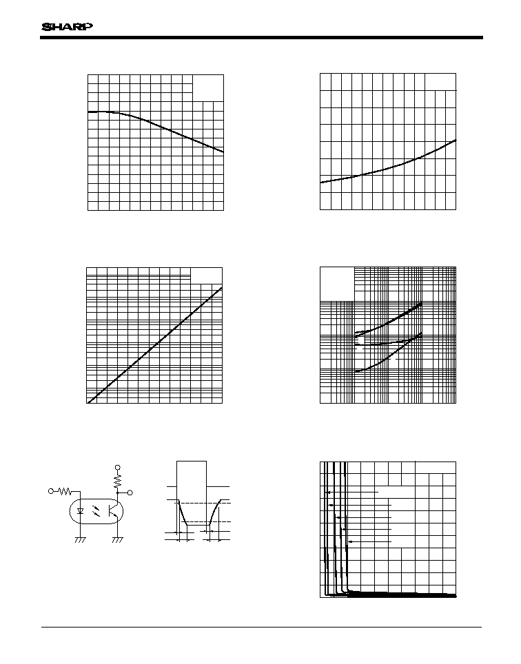
R
e
l
a
t
i
v
e
c
u
r
r
e
n
t
t
r
a
n
s
f
e
r
r
a
t
i
o
(
%
)
0
150
100
50
-
30
0
20
40
60
80
100
Ambient temperature T
a
(
∞
C)
I
F
=
5mA
V
CE
=
5V
R
e
s
p
o
n
s
e
t
i
m
e
(
µ
s
)
0.1
100
20
50
1000
200
500
10
2
5
1
0.2
0.5
0.01
0.1
1
10
100
t
r
t
d
t
f
t
s
Load resistance R
L
(k
)
V
CE
=
2V
I
C
=
2mA
T
a
=
25
∞
C
C
o
l
l
e
c
t
o
r
-
e
m
i
t
t
e
r
s
a
t
u
r
a
t
i
o
n
v
o
l
t
a
g
e
V
C
E
(
s
a
t
)
(
V
)
0.00
0.16
0.14
0.12
0.10
0.08
0.06
0.04
0.02
-
30
0
20
40
60
80
100
Ambient temperaturet T
a
(
∞
C)
I
F
=
20mA
I
C
=
1mA
C
o
l
l
e
c
t
o
r
d
a
r
k
c
u
r
r
e
n
t
I
C
E
O
(
A
)
10
-
11
10
-
5
5
10
-
6
5
10
-
7
5
10
-
8
5
10
-
9
5
10
-
10
5
-
30
0
20
40
60
80
100
Ambient temperature T
a
(
∞
C)
V
CE
=
20V
Fig.13 Test Circuit for Response Time
0
10
8
6
4
2
0
2
4
6
8
10
Forward current I
F
(mA)
7mA
5mA
3mA
1mA
C
o
l
l
e
c
t
o
r
-
e
m
i
t
t
e
r
s
a
t
u
r
a
t
i
o
n
v
o
l
t
a
g
e
V
C
E
(
s
a
t
)
(
V
)
T
a
=
25
∞
C
I
C
=
0.5mA
Fig.14 Collector-emitter Saturation Voltage
vs. Forward Current
Fig.9 Relative Current Transfer Ratio vs.
Ambient Temperature
Fig.10 Collector-emitter Saturation
Voltage vs. Ambient Temperature
Fig.12 Response Time vs. Load Resistance
Fig.11 Collector Dark Current vs. Ambient
Temperature
10%
Input
Output
Input
Output
90%
t
s
t
d
V
CC
R
D
R
L
t
f
t
r
PC3H7/PC3Q67Q
s
Precautions for Use
Please refer to the chapter "Precautions for Use".
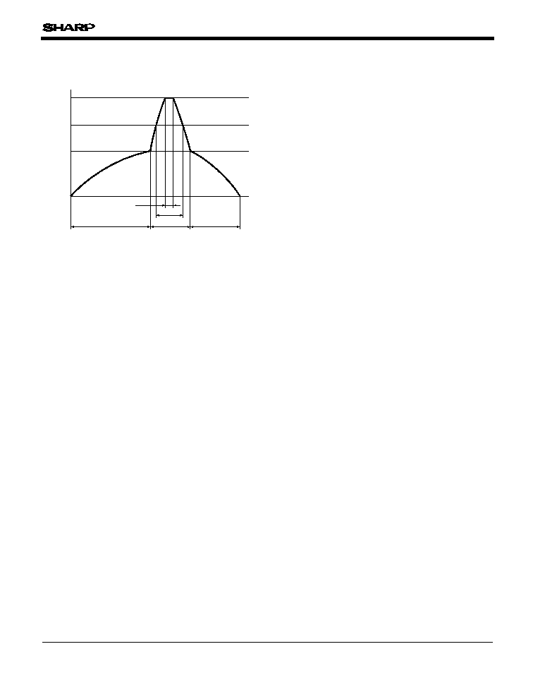
Fig.15 Reflow Soldering
25
∞
C
2min
230
∞
C
200
∞
C
180
∞
C
1min
1min
1.5min
30s
Only one time soldering is recommended within the temperature
profile shown below.

115
Application Circuits
NOTICE
qThe circuit application examples in this publication are provided to explain representative applications of
SHARP devices and are not intended to guarantee any circuit design or license any intellectual property
rights. SHARP takes no responsibility for any problems related to any intellectual property right of a
third party resulting from the use of SHARP's devices.
qContact SHARP in order to obtain the latest device specification sheets before using any SHARP device.
SHARP reserves the right to make changes in the specifications, characteristics, data, materials,
structure, and other contents described herein at any time without notice in order to improve design or
reliability. Manufacturing locations are also subject to change without notice.
qObserve the following points when using any devices in this publication. SHARP takes no responsibility
for damage caused by improper use of the devices which does not meet the conditions and absolute
maximum ratings to be used specified in the relevant specification sheet nor meet the following
conditions:
(i) The devices in this publication are designed for use in general electronic equipment designs such as:
--- Personal computers
--- Office automation equipment
--- Telecommunication equipment [terminal]
--- Test and measurement equipment
--- Industrial control
--- Audio visual equipment
--- Consumer electronics
(ii)Measures such as fail-safe function and redundant design should be taken to ensure reliability and
safety when SHARP devices are used for or in connection with equipment that requires higher
reliability such as:
--- Transportation control and safety equipment (i.e., aircraft, trains, automobiles, etc.)
--- Traffic signals
--- Gas leakage sensor breakers
--- Alarm equipment
--- Various safety devices, etc.
(iii)SHARP devices shall not be used for or in connection with equipment that requires an extremely
high level of reliability and safety such as:
--- Space applications
--- Telecommunication equipment [trunk lines]
--- Nuclear power control equipment
--- Medical and other life support equipment (e.g., scuba).
qContact a SHARP representative in advance when intending to use SHARP devices for any "specific"
applications other than those recommended by SHARP or when it is unclear which category mentioned
above controls the intended use.
qIf the SHARP devices listed in this publication fall within the scope of strategic products described in the
Foreign Exchange and Foreign Trade Control Law of Japan, it is necessary to obtain approval to export
such SHARP devices.
qThis publication is the proprietary product of SHARP and is copyrighted, with all rights reserved. Under
the copyright laws, no part of this publication may be reproduced or transmitted in any form or by any
means, electronic or mechanical, for any purpose, in whole or in part, without the express written
permission of SHARP. Express written permission is also required before any use of this publication
may be made by a third party.
qContact and consult with a SHARP representative if there are any questions about the contents of this
publication.