PC904
PC904
Symbol
Rating
Unit
I
A
50
mA
V
A
30
V
I
REF
10
mA
P
250
mW
V
CEO
35
V
V
ECO
6
V
I
C
50
mA
P
C
150
mW
P
tot
350
mW
V
iso
T
opr
- 25 to + 85
�C
T
stg
- 40 to + 125
�C
T
sol
260
�C
s
Features
1. Built-in voltage detection circuit
2. High isolation voltage between input and
3. Standard 8-pin dual-in-line package
s
Applications
*2 For 10 seconds
( Ta = 25�C)
s
Absolute Maximum Ratings
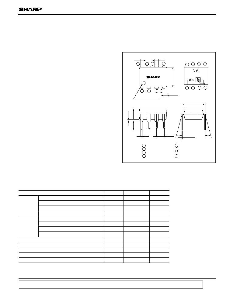
( Unit : mm)
connection diagram
Internal
PC904
output ( V
iso
Parameter
Input
Anode current
Anode voltage
Reference input current
Power dissipation
Output
Collector-emitter voltage
Emitter-collector voltage
Collector current
Collector power dissipation
Total power dissipation
*1
Isolation voltage
Operating temperature
Storage temperature
*2
Soldering temperature
data books, etc. Contact SHARP in order to obtain the latest version of the device specification sheets before using any SHARP's device.
"
"
In the absence of confirmation by device specification sheets, SHARP takes no responsibility for any defects that occur in equipment using any of SHARP's devices, shown in catalogs,
4. Recognizerd by UL, file No. E64380
1. Switching power supplies
1
2
3
4
8
7
6
5
1
2
3
4
5
6
7
8
1 Anode
2 Cathode
3 GND
4 Reference
5 NC
6 Emitter
7 Collector
8 NC
Built-in Voltage Detection
Circuit Type Photocoupler
s
Outline Dimensions
Primary side mark
5 000
*1 40 to 60%RH AC for 1 minute
g Lead forming type ( I type ) and taping reel type ( P type ) are also available. (
PC904I/PC904P
)
: 5 000V
rms
)
V
rms
=
0
�
to 13
�
6.5
�
0.5
1.2
�
0.3
0.85
�
0.3
0.8
�
0.2
7.62
�
0.3
0.26
�
0.1
2.54
�
0.25
0.5
�
0.1
3.0
�
0.5
3.5
�
0.5
0.5
TYP.
PC904
Conditions
V
K
= V
REF
, I
A
= 10mA
V
K
= V
REF
, I
A
= 10mA, Ta = - 25 to + 85�C
I
A
= 10mA,
V
A
= 30V - V
REF
I
A
= 10mA, R
3
= 10k
I
A
= 10mA, R
3
= 10k
, Ta = - 25 to + 85�C
V
K
= V
REF
V
A
= 30V, V
REF
= GND
V
K
= V
REF
, I
A
= 10mA
V
CE
= 35V
V
K
= V
REF
, I
A
= 5mA, V
CE
= 5V
V
K
= V
REF
, I
A
= 10mA, I
C
= 1mA
*3 V
REF (dev )
= V
REF ( MAX. )
- V
REF ( MIN. )
*4 I
REF (dev )
= I
REF ( MAX. )
- I
REF ( MIN. )
*5 CTR = I
C
/ I
A
x 100 (% )
MIN.
TYP.
MAX.
Unit
Fig.
2.40
2.495
2.60
V
1
-
8
40
mV
1
-
- 1.4
- 5
mV/V
2
-
2
10
�
A
3
-
0.4
3
�
A
3
-
1
2
mA
1
-
0.1
2
�
A
4
-
1.2
1.4
V
1
-
1 x 10
- 9
1 x 10
- 7
A
5
50
-
600
%
6
-
-
0.1
0.2
V
6
5 x 10
10
1 x 10
11
-
0.6
1.0
pF
-
-
s
Test Circuit
Fig. 1
Fig. 2
Model No.
Rank mark
CTR ( % )
A
50 to 150
B
100 to 300
C
250 to 600
A, B or C
50 to 600
( Ta = 25�C)
s
Electro-optical Characteristics
Parameter
Input
Reference voltage
reference voltage
*3
Temperature change in
Voltage variation ratio in
reference voltage
Reference input current
reference input current
*4
Temperature change in
Minimum drive current
Anode-cathode forward voltage
Output
Collector dark current
Transfer
charac-
teristics
Collector-emitter
saturation voltage
Isolation resistance
Floating capacitance
6
7
2
1
4
3
V
V
A
3
4
1
2
7
6
Ia
V
K
V
CC
V
REF
V
F
V
CC
V
A
R
1
R
2
V
REF
I
A
PC904A
PC904B
PC904C
PC904
*5
Current transfer ratio
Symbol
V
REF
V
REF ( dev )
V
REF
/
V
A
I
REF
I
REF ( dev )
I
MIN
I
OFF
V
F
I
CEO
CTR
V
CE( sat )
R
ISO
C
f
OFF-state anode current
V = 0, f = 1kHz
Classification table of current transfer ratio is shown below. ( 4 models )
40 to 60% RH, DC500V
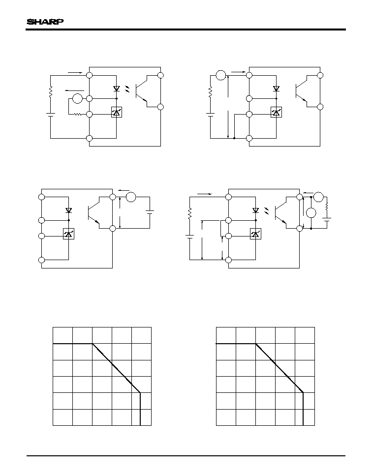
Fig. 3
Fig. 4
Fig. 5
Fig. 6
PC904
A
3
4
1
2
7
6
A
3
4
1
2
7
6
I
A
V
CC
R
3
I
REF
V
A
V
CC
I
OFF
3
4
1
2
7
6
3
4
1
2
7
6
A
V
A
I
CEO
V
CE
V
CC
V
K
V
REF
I
A
V
CE
I
C
0
- 25
100
10
20
30
40
50
60
0
25
50
75 85
Anode current I
A
(
mA
)
Ambient temperature T
a
(�C)
0
- 25
100
50
100
150
200
250
300
0
25
50
75 85
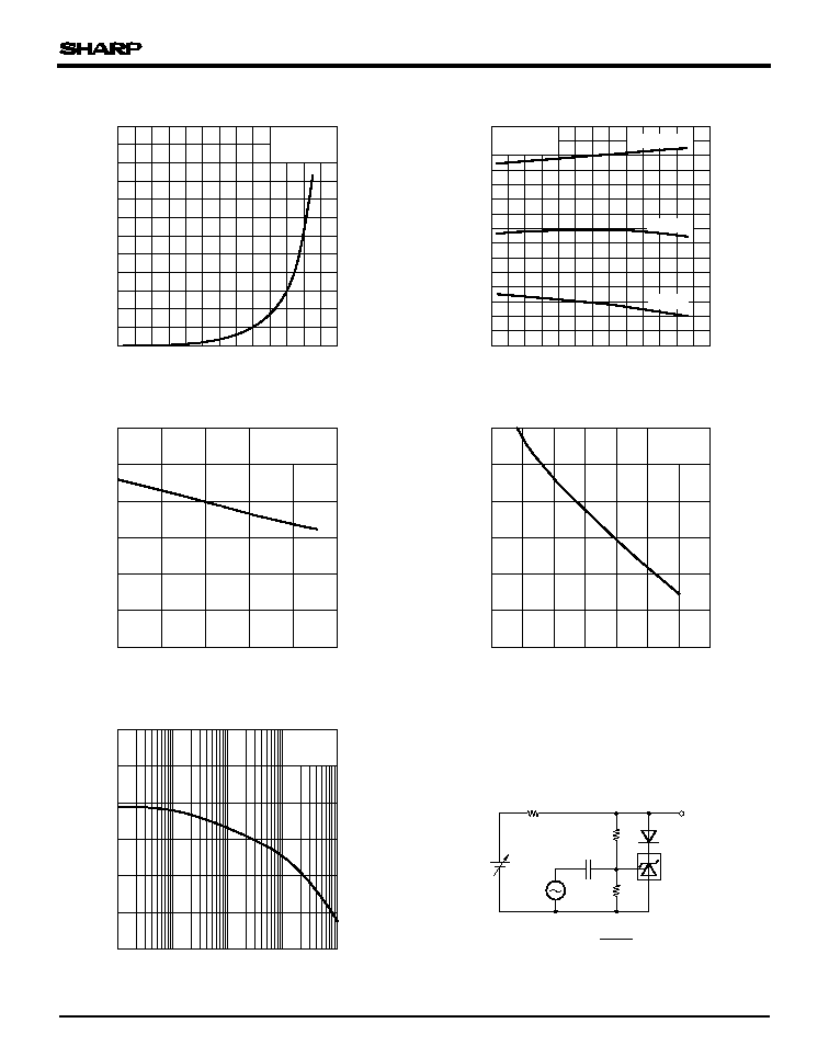
Fig. 8 Input Power Dissipation vs.
Ambient Temperature
Input power dissipation P
(
mW
)
Ambient temperature T
a
(�C)
Fig. 7 Anode Current vs. Ambient
Temperature
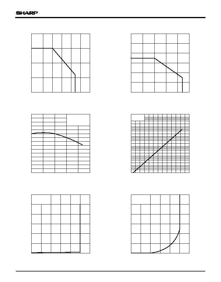
PC904
0
0
125
100
200
50
150
25
50
75
100
Ambient Temperature
- 25
85
0
300
0
25
50
75
100
85
600
200
100
500
400
350
Power dissipation P
tot
(
mW
)
Ambient temperature T
a
(�C)
50
0
100
150
0
25
100
75
50
Relative current transfer ratio
(
%
)
Fig.11 Relative Current Transfer Ratio vs.
Ambient Temperature
Ambient temperature T
a
(�C)
20
0
40
60
80
5
5
5
5
5
100
Fig.12 Collector Dark Current vs.
Ambient Temperature
Ambient temperature T
a
( �C)
Collector dark current I
CEO
(
A
)
0
0
3
10
20
30
40
50
1
2
Anode current I
A
(
mA
)
Reference voltage V
REF
(V)
Voltage
0
0
3
200
400
600
800
1
2
Anode current I
A
Reference voltage V
REF
(V)
Voltage
Collector power dissipation P
C
(
mW
)
Ambient temperature T
a
(�C)
Fig.10 Power Dissipation vs. Ambient
Temperature
V
CE
= 35V
5
V
K
= V
REF
I
A
= 5mA
V
CE
= 5V
V
K
= V
REF
T
a
= 25�C
V
K
= V
REF
T
a
= 25�C
Fig. 9 Collector Power Dissipation vs.
Fig.13-a Anode Current vs. Reference
Fig.13-b Anode Current vs. Reference
(
�
A
)
- 30
10
- 11
10
- 10
10
- 9
10
- 8
10
- 7
10
- 6
10
- 5
1 200
1 000
- 25
- 25
PC904
0
- 30
100
0
20
40
60
80
5
10
Ambient Temperature
OFF
(
�
A
)
Ambient temperature T
a
(�C)
Fig.14 OFF-state Anode Current vs.
- 30
100
0
20
40
60
80
2.40
2.50
2.60
2.495V
2.40V
Ambient Temperature
REF
Ambient temperature T
a
(�C)
Fig.15 Reference Voltage vs.
V
REF
= 2.60V
0
- 25
100
1
2
3
0
25
50
75
Ambient Temperature
Reference input current I
REF
(
�
A
)
Ambient temperature T
a
(�C)
Fig.16 Reference Input Current vs.
I
A
= 10mA
- 30
0
- 20
- 10
0
5
10
15
20
25
30
35
Anode Voltage
REF
(
mV
)
Anode voltage V
A
(V)
Fig.17 Reference Voltage Change vs.
- 20
0.1
0
20
40
60
80
100
1
10
100
Voltage gain
(1
) A
V1
(
dB
)
10
�
F
620
10k
10k
f
Test Circuit for Voltage Gain
(
1
)
vs.
Frequency
V
in
V
o
V
in
A
V1
V
o
V
A
= 30V
V
REF
= GND
I
A
= 10mA
I
A
= 10mA
T
a
= 25�C
I
F
= 2mA
T
a
= 25�C
OFF-state anode current I
V
K
= V
REF
(
V
)
Reference voltage V
Reference voltage change
V
Frequency f ( kHz)
Fig.18-a Voltage Gain (1) vs. Frequency
=
20 log
1 000
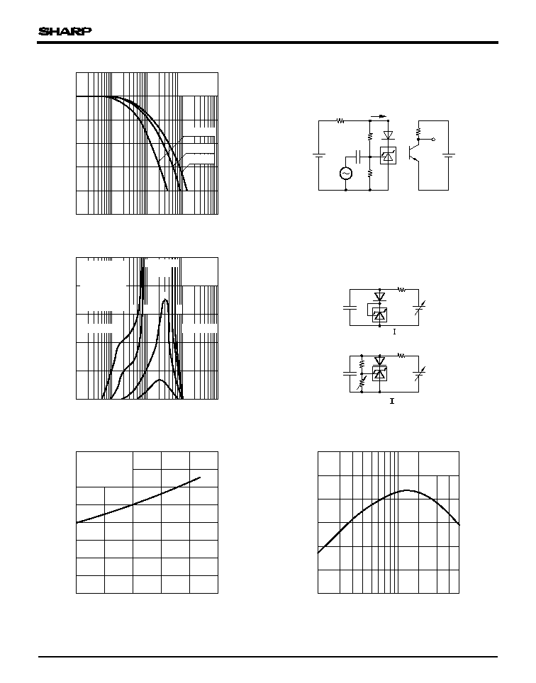
PC904
- 50
0.1
- 40
- 30
- 20
- 10
0
10
1
10
100
100
1k
Voltage gain
(2
) A
V2
(
dB
)
0
10
20
30
40
50
10
Anode current I
A
(
mA
)
Load capacitance C
L
(
�
F )
0
0.02
0.04
0.06
0.08
0.10
0.12
0.14
0.16
- 25
0
25
50
75
100
Ambient temperature T
a
(�C)
0
50
1
10
50
300
20
2
100
150
200
250
5
Current transfer ratio CTR
(%)
Anode Current
Anode Current I
A
( mA )
Fig.21 Current Transfer Ratio vs.
s
Precautions for Use
10
�
F
620
10k
10
f
k
Test Circuit for Voltage Gain (2) vs.
Frequency
V
in
V
o
R
L
I
A
10k
150
150
Test Circuit for Anode Current vs.
Load Capacitance
C
L
C
L
Handle this product the same as with other integrated circuits against static electricity.
I
A
= 2mA
I
C
= 1.7mA
T
a
= 25�C
R
L
= 10k
10
- 3
10
- 2
10
- 1
Fig.20 Collector-emitter Saturation Voltage
vs. Ambient Temperature
V
CE
( sat
)
(
V
)
V
K
= V
REF
I
C
= 1mA
I
A
= 10mA
V
K
= V
REF
V
CE
= 5V
T
a
= 25�C
Fig.18-b Voltage Gain (2) vs. Frequency
Frequency f ( kHz)
Oscilating
Stable area
D
Stable area
C
A
B
B
A
area
A��� V
K
= V
REF
B��� V
A
= 5V
( at I
A
= 10mA )
C��� V
A
= 10V
( at I
A
= 10mA )
D��� V
A
= 15V
( at I
A
= 10mA )
T
a
= 25�C
Collector-emitter saturation voltage
Test circuit
( B, C, D )
Test circuit
(A)
1 000
As for other general cautions, refer to the chapter " Precautions for Use "
Fig.19 Anode Current vs. Load Capacitance
1
q

115
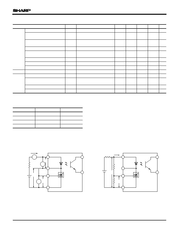
Application Circuits
NOTICE
qThe circuit application examples in this publication are provided to explain representative applications of
SHARP devices and are not intended to guarantee any circuit design or license any intellectual property
rights. SHARP takes no responsibility for any problems related to any intellectual property right of a
third party resulting from the use of SHARP's devices.
qContact SHARP in order to obtain the latest device specification sheets before using any SHARP device.
SHARP reserves the right to make changes in the specifications, characteristics, data, materials,
structure, and other contents described herein at any time without notice in order to improve design or
reliability. Manufacturing locations are also subject to change without notice.
qObserve the following points when using any devices in this publication. SHARP takes no responsibility
for damage caused by improper use of the devices which does not meet the conditions and absolute
maximum ratings to be used specified in the relevant specification sheet nor meet the following
conditions:
(i) The devices in this publication are designed for use in general electronic equipment designs such as:
--- Personal computers
--- Office automation equipment
--- Telecommunication equipment [terminal]
--- Test and measurement equipment
--- Industrial control
--- Audio visual equipment
--- Consumer electronics
(ii)Measures such as fail-safe function and redundant design should be taken to ensure reliability and
safety when SHARP devices are used for or in connection with equipment that requires higher
reliability such as:
--- Transportation control and safety equipment (i.e., aircraft, trains, automobiles, etc.)
--- Traffic signals
--- Gas leakage sensor breakers
--- Alarm equipment
--- Various safety devices, etc.
(iii)SHARP devices shall not be used for or in connection with equipment that requires an extremely
high level of reliability and safety such as:
--- Space applications
--- Telecommunication equipment [trunk lines]
--- Nuclear power control equipment
--- Medical and other life support equipment (e.g., scuba).
qContact a SHARP representative in advance when intending to use SHARP devices for any "specific"
applications other than those recommended by SHARP or when it is unclear which category mentioned
above controls the intended use.
qIf the SHARP devices listed in this publication fall within the scope of strategic products described in the
Foreign Exchange and Foreign Trade Control Law of Japan, it is necessary to obtain approval to export
such SHARP devices.
qThis publication is the proprietary product of SHARP and is copyrighted, with all rights reserved. Under
the copyright laws, no part of this publication may be reproduced or transmitted in any form or by any
means, electronic or mechanical, for any purpose, in whole or in part, without the express written
permission of SHARP. Express written permission is also required before any use of this publication
may be made by a third party.
qContact and consult with a SHARP representative if there are any questions about the contents of this
publication.