 | –≠–ª–µ–∫—Ç—Ä–æ–Ω–Ω—ã–π –∫–æ–º–ø–æ–Ω–µ–Ω—Ç: PQ1R25 | –°–∫–∞—á–∞—Ç—å:  PDF PDF  ZIP ZIP |
36
Low Power-Loss Voltage Regulators
PQ1R30 Series
s
Features
q
Compact surface mount package(3.4 x 2.2 x 1.2mm)
q
Low power-loss
(Dropout voltage: TYP.0.16V/MAX. 0.26V at Io=60mA)
q
High ripple rejection(TYP.55dB)
q
Low current operation type
(Dissipation current at no load: TYP. 170µA)
q
Built-in ON/OFF control function
(Dissipation current at OFF-state: MAX. 0.1µA)
q
Overcurrent, overheat protection functions
s
Applications
q
Cellular phones
q
Cordless phones
q
Personal information tools(PDA)
q
Cameras/Camcoders
q
PCMCIA cards for notebook PCs
s
Model Line-ups
s
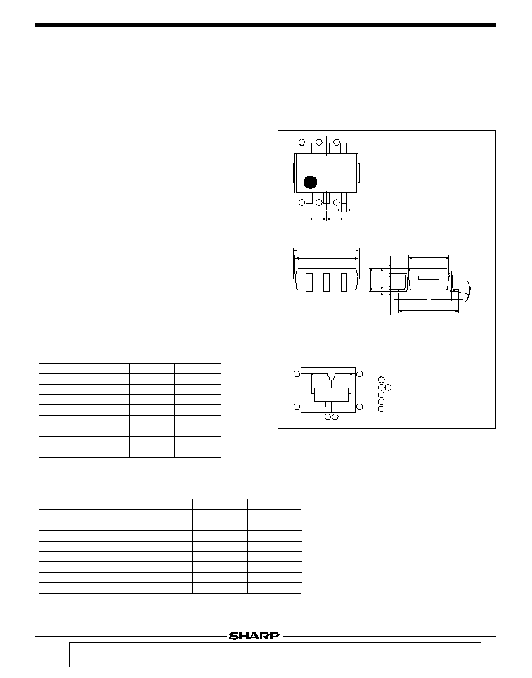
Outline Dimensions
(Unit : mm)
Low Output Current, Compact Surface Mount Type Low Power-Loss Voltage Regulators
∑ Please refer to the chapter " Handling Precautions ".
PQ1R30 Series
Output Voltage
2.2V
2.5V
2.7V
2.8V
2.9V
3.0V
3.1V
3.3V
Model No.
PQ1R22
PQ1R25
PQ1R27
PQ1R28
PQ1R29
PQ1R30
PQ1R31
PQ1R33
Output Voltage
3.4V
3.6V
3.8V
4.0V
4.7V
4.9V
5.0V
5.2V
Model No.
PQ1R34
PQ1R36
PQ1R38
PQ1R40
PQ1R47
PQ1R49
PQ1R50
PQ1R52
f
It is available for every 0.1V(1.8V to 5.5V)
s
Absolute Maximum Ratings
Parameter
Symbol
Rating
Unit
16
16
240
400
150
≠30 to +80
≠55 to +150
260 (For 10s)
V
V
mA
mW
∞C
∞C
∞C
∞C
f1
f1
f2
f3
f1
All are open except GND and applicable terminals.
f2
At surface-mounted condition
f3
Overheat protection may operate at 125<=T
j
<=150∞C.
(T
a
=25∞C)
Input voltage
V
IN
ON/OFF control terminal voltage
Vc
Output current
Io
Power dissipation
P
D
Junction temperature
T
j
Operating temperature
T
opr
Storage temperature
T
stg
Soldering temperature
T
sol
1
6
6
5
4
1
2
3
1
4
3
2 5
2
3
4
6
5
DC output (V
o
)
DC input (V
IN
)
GND
Noise reduction (N
r
)
ON/OFF control terminal(V
c
)
Specific IC
(0.95) (0.95)
6≠0.32
±
0.1
3.8MAX
(3.4)
2.2
±
0.2
3.3
±
0.3
0.2MIN 0.2MIN
1.2
±
0.2
0.15
±
0.1
(0.3)
0
~
0.1
1.4MAX
15 MAX
∞
( ) :Typical dimensions
1 R 3 0
Internal connection diagram
Notice
In the absence of confirmation by device specification sheets,SHARP takes no responsibility for any defects that may occur in equipment using any SHARP
devices shown in catalogs,data books,etc.Contact SHARP in order to obtain the latest device specification sheets before using any SHARP device.
Internet Internet address for Electronic Components Group http://www.sharp.co.jp/ecg/
37
Low Power-Loss Voltage Regulators
PQ1R30 Series
s
Electrical Characteristics
Dropout voltage
ON-state voltage for control
ON-state current for control
OFF-state voltage for control
Quiescent current
Output OFF-state dissipation current
Response time(Rise time)
Noise control terminal voltage
Parameter
Symbol
Conditions
MIN.
TYP.
MAX.
Unit
Output voltage
≠≠
V
≠≠
I
O
=5mA to 60mA
I
O
=5mA to 100mA
I
O
=5mA to 150mA
I
O
=60mA,
f6
I
O
=0mA
f5
mV
10Hz<f<100kHz, C
n
=0.1
µ
F, I
O
=30mA
I
O
=10mA, T
j
=≠25 to +75∞C
V
i
=V
O
(TYP)+1V to V
O
(TYP)+6V
%/∞C
≠≠
dB
I
O
=150mA,
f6
µ
Vrms
f7
V
≠≠
≠≠
≠≠
V
I
O
=30mA, V
C
=0®1.8V
ms
V
V
C
=1.8V
V
IN
=8V, V
C
=0.4V
µ
A
V
µ
A
µ
A
mA
mA
mV
f4
V
IN
=Vo (TYP)+1.0V
f5
Output current shall be the value when output voltage lowers 0.3V from the voltage at Io=30mA.
f6
Dropout voltage when output voltage lowers 5% from the voltage at V
IN
=Vo+1V.
f7
In case that the control terminal is non-connection, output voltage should be OFF-state.
(Unless otherwise specified,
f4
Io=30mA, Vc=1.8V, Ta=25∞C)
180
≠≠
≠≠
≠≠
≠≠
≠≠
≠≠
≠≠
≠≠
≠≠
1.8
≠≠
≠≠
≠≠
≠≠
≠≠
≠≠
Refer to the following table.
240
≠≠
10
20
40
3.0
0.05
55
Refer to the following table.
0.16
0.29
≠≠
12
≠≠
170
≠≠
0.3
1.25
≠≠
150
50
100
160
20
≠≠
≠≠
0.26
0.4
≠≠
30
0.6
350
0.1
≠≠
≠≠
V
O
I
O
≠≠
R
eg
L
R
eg
I
T
C
V
O
RR
Vno
V
i
-
O
(1)
V
i
-
O
(2)
V
C
(
ON
)
I
C
(
ON
)
V
C
(
OFF
)
I
q
I
qs
T
r
≠≠
Output current
Recommended output current
Load regulation
Line regulation
Temperature coefficient of output voltage
Ripple rejection
Output noise voltage
1
s
Output Voltage Line-ups
Model No.
Symbol
MIN.
TYP.
MAX.
Unit
V
V
V
V
V
V
V
V
V
V
V
V
V
V
V
V
(V
IN
=Vo(TYP)+1.0V, Io=30mA, Vc=1.8V, Ta=25∞C)
2.120
2.420
2.620
2.720
2.820
2.920
3.020
3.215
3.315
3.510
3.705
3.900
4.580
4.775
4.875
5.070
2.2
2.5
2.7
2.8
2.9
3.0
3.1
3.3
3.4
3.6
3.8
4.0
4.7
4.9
5.0
5.2
2.280
2.580
2.780
2.880
2.980
3.080
3.180
3.385
3.485
3.690
3.895
4.100
4.820
5.025
5.125
5.330
V
O
V
O
V
O
V
O
V
O
V
O
V
O
V
O
V
O
V
O
V
O
V
O
V
O
V
O
V
O
V
O
PQ1R22
PQ1R25
PQ1R27
PQ1R28
PQ1R29
PQ1R30
PQ1R31
PQ1R33
PQ1R34
PQ1R36
PQ1R38
PQ1R40
PQ1R47
PQ1R49
PQ1R50
PQ1R52
s
Output Noise Voltage Line-ups
Model No.
Symbol
MIN.
TYP.
MAX.
Unit
µ
Vrms
µ
Vrms
µ
Vrms
µ
Vrms
µ
Vrms
µ
Vrms
µ
Vrms
µ
Vrms
µ
Vrms
µ
Vrms
µ
Vrms
µ
Vrms
µ
Vrms
µ
Vrms
µ
Vrms
µ
Vrms
(V
IN
=Vo(TYP)+1.0V, Io=30mA, Vc=1.8V, Cn=0.1
µ
F, 10Hz<f<100kHz, Ta=25∞C)
≠≠
≠≠
≠≠
≠≠
≠≠
≠≠
≠≠
≠≠
≠≠
≠≠
≠≠
≠≠
≠≠
≠≠
≠≠
≠≠
20
25
25
25
25
30
30
30
30
35
35
40
45
45
50
50
≠≠
≠≠
≠≠
≠≠
≠≠
≠≠
≠≠
≠≠
≠≠
≠≠
≠≠
≠≠
≠≠
≠≠
≠≠
≠≠
Vno
Vno
Vno
Vno
Vno
Vno
Vno
Vno
Vno
Vno
Vno
Vno
Vno
Vno
Vno
Vno
PQ1R22
PQ1R25
PQ1R27
PQ1R28
PQ1R29
PQ1R30
PQ1R31
PQ1R33
PQ1R34
PQ1R36
PQ1R38
PQ1R40
PQ1R47
PQ1R49
PQ1R50
PQ1R52
38
Low Power-Loss Voltage Regulators
PQ1R30 Series
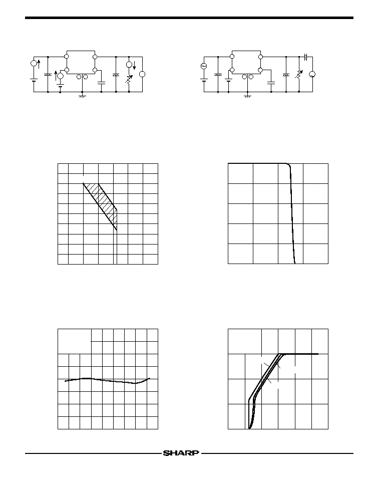
Fig. 4 Overcurrent Protection Characteristics
(Typical Value)
Fig. 3 Power Dissipation vs. Ambient
Temperature
Note) Oblique line portion : Overheat protection may operate in this area.
0
≠20 0
P
D
80
50
100
150
500
400
300
200
100
Power dissipation P
D
(mW)
Ambient temperature T
a
(∞C)
Note) Oblique line portion : Overheat protection may operate in this area.
100
80
40
60
20
0
Relative output voltage (%)
Output current I
O
(A)
0
0.1
0.2
0.3
0.4
Fig. 6 Output Voltage vs. Input Voltage
(PQ1R30) (Typical Value)
Fig. 5 Output Voltage Deviation vs. Junction
Temperature (PQ1R30) (Typical Value)
Fig. 1 Test Circuit
Fig. 2 Test Circuit of Ripple Rejection
I
c(
ON
)
V
A
A
V
IN
V
c
I
q,
I
qs
I
O
V
O
R
L
10
µ
F
1
µ
F
0.1
µ
F
+
+
6
3
2
5
4
A
1
V
IN
V
c
R
L
10
µ
F
1
µ
F
0.1
µ
F
+
+
e
o
+
V
6
3
2
5
4
1
f
=400Hz(sine wave)
ei
=100mV
rms
V
IN
=Vo(TYP)+1.0V
I
o
=10mA
RR=20 log(e
i
/e
o
)
e
i
80
20
0
40
60
≠40
≠20
≠60
≠80
Output voltage deviation
V
O
(mV)
Junction temperature Tj (∞C)
≠40
0
20
≠20
40 60
100 120
80
140
V
IN
=4.0V
I
O
=10mA
V
C
=1.8V
C
O
=10
µ
F
4.0
2.0
3.0
1.0
0
Output voltage Vo(V)
Input voltage V
IN
(V)
0
3.0
5.0
4.0
2.0
1.0
6.0
C
IN
=1
µ
F
C
O
=10
µ
F
R
L
=
R
L
=40
R
L
=20
39
Low Power-Loss Voltage Regulators
PQ1R30 Series
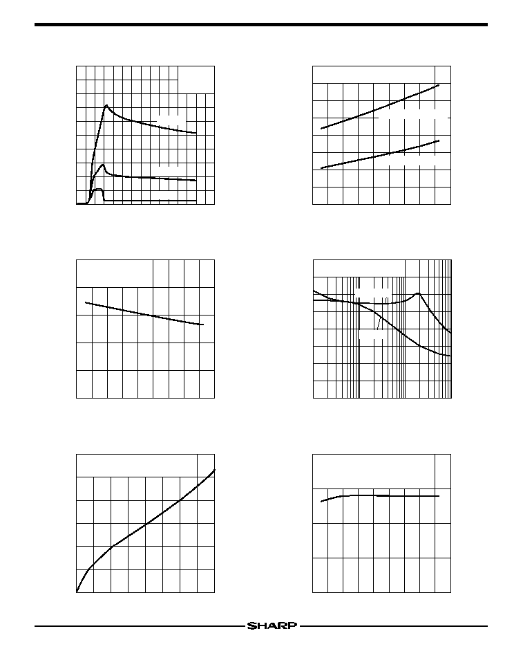
Fig.10 Ripple Rejection vs. Input Ripple
Frequency
Fig. 9 Quiescent Current vs. Junction
Temperature
Fig.12 Output Peak Current vs. Junction
Temperature
Fig.11 Dropout Voltage vs. Output Current
Fig. 8 Dropout Voltage vs. Junction
Temperature (PQ1R30) (Typical Value)
Fig. 7 Circuit Operating Current vs. Input
Voltage (PQ1R30) (Typical Value)
C
IN
=1
µ
F
C
O
=10
µ
F
10.0
5.0
4.0
7.0
9.0
8.0
6.0
2.0
3.0
1.0
0
Circuit operating current Ibias (mA)
Input voltage V
IN
(V)
0
5.0
10.0
15.0
R
L
=
R
L
=20
R
L
=40
0.4
0.35
0.25
0.15
0.05
0.2
0.3
0.1
0
Dropout voltage Vi-o (V)
Junction temperature Tj (∞C)
≠40
80
120
100
40
0
≠20
20
60
140
V
IN
: Voltage when output voltage is 95%, V
C
=1.8V
Vi-o(2) : Io=150mA
Vi-o(1) : Io=60mA
250
200
100
50
150
0
Quiescent current Iq (
µ
A)
Junction temperature Tj (∞C)
≠40
80
120
100
40
0
≠20
20
60
140
V
IN=
Vo(TYP)+1.0V,
Vc=1.8V, Io=0A
Ta=25∞C, V
IN
=4.0V,
Io=10mA (300
), Co=10
µ
F
0
0.1
10
1
100
10
20
30
40
50
60
70
80
Ripple rejection RR (dB)
Input ripple frequency f
(kHz)
Cn : No
Cn=0.1
µ
F
0.3
0.25
0.15
0.2
0.1
Output peak current Iop(A)
Junction temperature Tj (∞C)
≠40
80
120
100
40
0
≠20
20
60
140
V
IN
: Vo(TYP)+1.0V, Vc=1.8V, lop :
Output current when output voltage lowers
0.3V in comparison with the value at Io=30mA
300
250
150
50
100
200
0
Dropout voltage Vi-o (V)
Output current Io (mA)
0
120 140
80
40
20
60
100
160
Ta=25∞C, V
C
=1.8V, V
IN
: Voltage when
output voltage is 95%.
40
Low Power-Loss Voltage Regulators
PQ1R30 Series
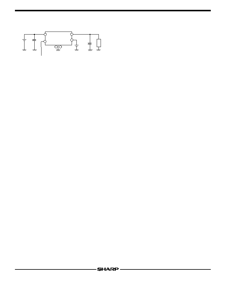
s
Typical Application
C
O
V
IN
C
IN
+
+
Vo
Load
2
5
4
ON/OFF signal
High : Output ON
Low or Open : Output OFF
1
6
3
0.1
µ
F