PR26MF11NSZ Series/
PR36MF11NSZ Series
PR26MF11NSZ Series/PR36MF11NSZ Series
s
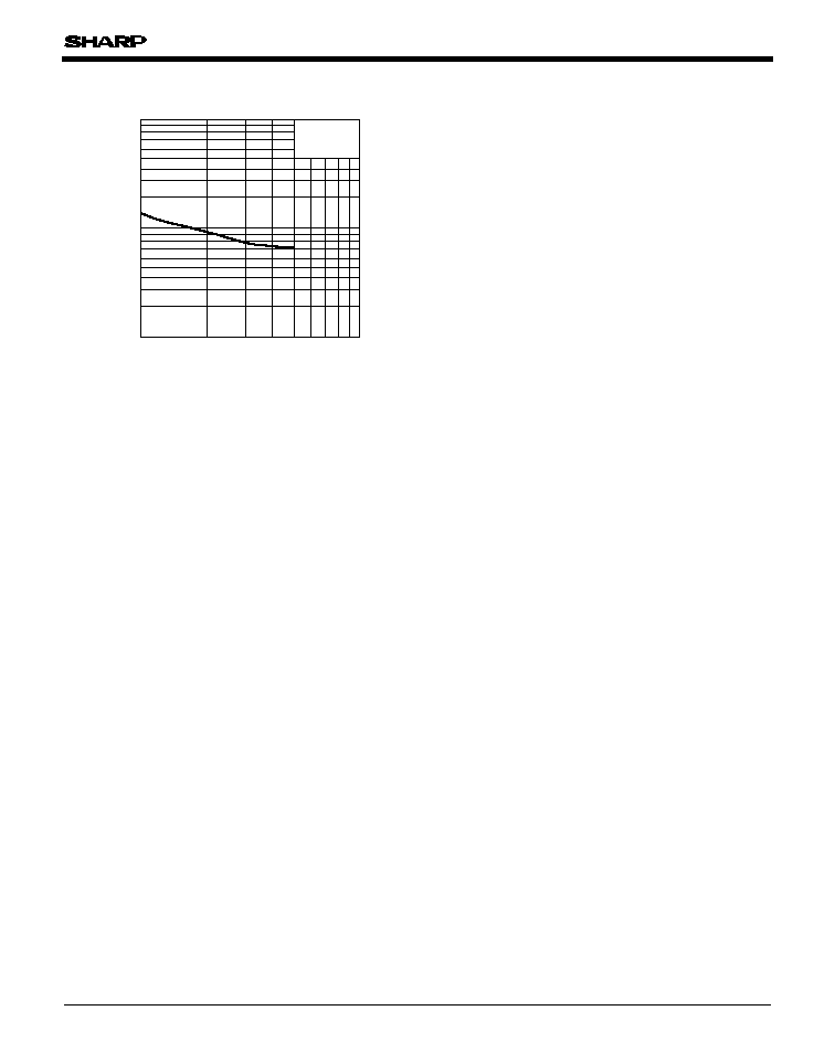
Model Line-up
s
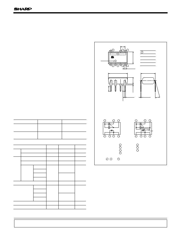
Outline Dimensions
(Unit : mm)
For 200V line
PR36MF11NSZ
PR36MF21NSZ
For 100V line
No built-in zero-
cross circuit
Built-in zero-
cross circuit
PR26MF11NSZ
PR26MF21NSZ
s
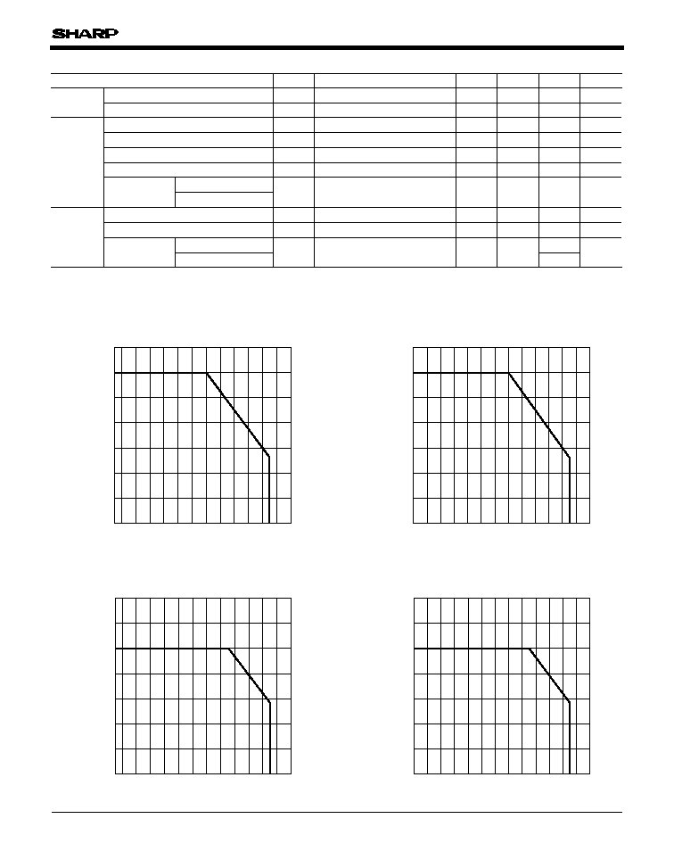
Absolute Maximum Ratings
*1 The derating factors of absolute maximum ratings due to ambient temperature are
shown in Fig.1, 2
*2 AC for 1 min, 40 to 60%RH, f
=
60Hz
Parameter
Symbol
Rating
Unit
Forward current
I
F
50
0.6
mA
Reverse voltage
RMS ON-state current
Repetitive
peak
OFF-state
voltage
Peak one cycle surge current
Input
PR26MF11NSZ
PR26MF21NSZ
PR36MF11NSZ
PR36MF21NSZ
Output
V
R
6
V
A
V
I
surge
6 (50Hz sine wave)
600
400
A
V
DRM
V
iso (rms)
I
T (rms)
kV
Isolation voltage
Operating
temperature
T
opr
-
40 to
+
125
-
25 to
+
85
-
30 to
+
85
�
C
�
C
Storage temperature
T
stg
*2
*1
*1
Soldering temperature
T
sol
260 (For 10s)
4.0
�
C
(Ta
=
25
�
C)
PR26MF11NSZ
PR26MF21NSZ
PR36MF11NSZ
PR36MF21NSZ
1. Various types of home appliances
s
Features
s
Applications
8-Pin DIP Type SSR for Low
Power Control
1. Compact 8-pin dual-in-line package type
2. RMS ON-state current I
T(rms)
:0.6A
3. Built-in zero-cross circuit
(PR26MF21NSZ/PR36MF21NSZ)
4. High repetitive peak OFF-state voltage
PR26MF11NSZ/PR26MF21NSZ
V
DRM
:MIN. 400V
PR36MF11NSZ/PR36MF21NSZ
V
DRM
:MIN. 600V
5. Isolation voltage between input and output
(V
iso(rms)
:4kV)
6. Recognized by UL, file No. E94758
(PR26MF11NSZ/PR36MF11NSZ)
7. Approved by CSA No. LR63705
(PR26MF11NSZ/PR36MF11NSZ)
8.
PR26MF21NSZ/PR36MF21NSZ
:under preparation
for UL and CSA
Notice
In the absence of confirmation by device specification sheets, SHARP takes no responsibility for any defects that may occur in equipment using any SHARP
devices shown in catalogs, data books, etc. Contact SHARP in order to obtain the latest device specification sheets before using any SHARP device.
Internet
Internet address for Electronic Components Group http://www.sharp.co.jp/ecg/
Terminal , and are common ones of cathode.To radiate the
heat, solder all of the lead pins on the pattern of PWB.
Internal connection Diagram
PR26MF21NSZ/
PR36MF21NSZ
PR26MF11NSZ/
PR36MF11NSZ
Zero-cross
circuit
Anode
mark
(Model No.)
R26MF1
R26MF2
R36MF1
R36MF2
Zero-cross circuit for (PR26MF21NSZ/PR36MF21NSZ)
:
0 to 13
�
2.54
�
0.25
6.5
�
0.5
1.2
�
0.3
9.66
�
0.5
3.5
�
0.5
7.62
�
0.3
2.9
�
0.5
3.25
�
0.5
0.5
�
0.1
0.5
TYP.
0.26
�
0.1
8
A
A
6
5
1
2
3
4
1
1
3
4
8
6
5
2
3
4
1
8
6
5
2
3
4
Cathode
Anode
Cathode
Cathode
G
T
1
T
2
1
2
3
4
5
6
8
PR26MF11NSZ Series/PR36MF11NSZ Series
Parameter
Conditions
Input
Forward voltage
I
F
=
20mA
I
F
=
15mA, R load
ON-state voltage
Output
V
D
=
6V
Critical rate of rise of OFF-state voltage
V
D
=
1/
-
2
�
V
DRM
Transfer
charac-
teristics
Minimum trigger current
V
D
=
6V, R
L
=
100
V
D
=
6V, R
L
=
100
, I
F
=
20mA
MIN.
-
-
-
100
5
�
10
10
TYP.
1.2
-
-
10
11
MAX.
1.4
3.0
25
-
-
-
Holding current
Symbol
V
F
V
T
V
OX
I
H
dV/dt
I
FT
Isolation resistance
R
ISO
I
T
=
0.6A
Unit
V
Reverse current
V
R
=3V
V
D
=V
DRM
I
R
Repetitive peak OFF-state current
I
DRM
mA
-
-
10
�
A
-
-
100
�
A
V/
�
s
-
-
10
mA
V
-
-
35
V
(Ta
=
25�C)
Turn-on time
-
-
100
50
t
on
�
s
DC
=
500V, 40 to 60%RH
PR26MF11NSZ/PR36MF11NSZ
PR26MF21NSZ/PR36MF21NSZ
PR26MF21NSZ
PR36MF21NSZ
Zero-cross
voltage
s
Electrical Characteristics
0
0.1
0.2
0.3
0.4
0.5
0.6
0.7
-
25
-
20
-
10 0
10 20 30 40 50 60 70 80 90 100
RMS ON-state current I
T (rms)
(A)
Ambient temperature T
a
(�C)
0
10
20
30
40
50
60
70
-
25
-
20
-
10 0
10 20 30 40 50 60 70 80 90 100
Forward current I
F
(mA)
Ambient temperature T
a
(�C)
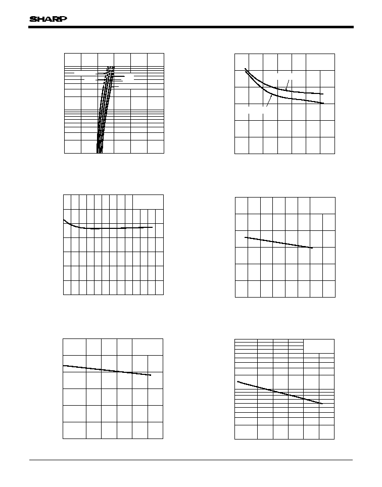
Fig.1
RMS ON-state Current vs. Ambient
Temperature (PR26MF11NSZ/PR36MF11NSZ)
Fig.3
Forward Current vs. Ambient Temperature
(PR26MF11NSZ/PR36MF11NSZ)
-
30
-
20
-
10 0
10 20 30 40 50 60 70 80 90 100
0
0.1
0.2
0.3
0.4
0.5
0.6
0.7
RMS ON-state current I
T (rms)
(A)
Ambient temperature T
a
(�C)
0
10
20
30
40
50
60
70
-
30
-
20
-
10 0
10 20 30 40 50 60 70 80 90 100
Forward current I
F
(mA)
Ambient temperature T
a
(�C)
Fig.2
RMS ON-state Current vs. Ambient
Temperature (PR26MF21NSZ/PR36MF21NSZ)
Fig.4
Forward Current vs. Ambient Temperature
(PR29MF21NSZ/PR39MF21NSZ)
PR26MF11NSZ Series/PR36MF11NSZ Series
1
1.2
1.1
1.4
1.3
1.5
1.6
-
40
0
-
20
20
40
60
80
120
100
ON-state voltage V
T
(V)
Ambient temperature T
a
(�C)
I
T
=
0.6A
10
10
2
10
3
-
30
0
20
40
60
80
100
Relative holding current I
H
(t
�
C) / I
H
(25
�
C)
�
100%
Ambient temperature T
a
(�C)
V
D
=
6V
Fig.8 ON-state Voltage vs. Ambient Temperature
(PR26MF11NSZ/PR36MF11NSZ)
Fig.10
Relative Holding Current vs. Ambient
Temprature (PR26MF11NSZ/PR36MF11NSZ)
200
50
20
5
2
1
100
10
0.5
0
1
1.5
2
2.5
3
-
25�C
50�C
25�C
0�C
Forward current I
F
(mA)
Forward voltage V
F
(V)
T
a
=
75�C
0
2
4
6
8
12
10
-
40
-
20
0
20
40
60
80
100
Minimum trigger current I
FT
(mA)
Ambient temperature T
a
(�C)
V
D
=
6V
R
L
=
100
PR26MF11NSZ
PR36MF11NSZ
Fig.5
Forward Current vs. Forward Voltage
Fig.6
Minimum Trigger Current vs. Ambient
Temperature
Fig.9 ON-state Voltage vs. Ambient Temperature
(PR26MF21NSZ/PR36MF21NSZ)
Fig.7 Minimum Trigger Current vs. Ambient Temperature
(PR26MF21NSZ/PR36MF21NSZ)
0.8
1
0.9
1.2
1.1
1.3
1.4
-
30
0
20
40
60
80
100
ON-state voltage V
T
(V)
Ambient temperature T
a
(�C)
I
T
=
0.6A
0
7
6
5
4
3
2
1
Minimum trigger current I
FT
(mA)
Ambient temperature T
a
(
�
C)
V
D
=6
V
R
L
=
100
-
30
0
-
20
-
10
20
40
60
80
100
10
30
50
70
90
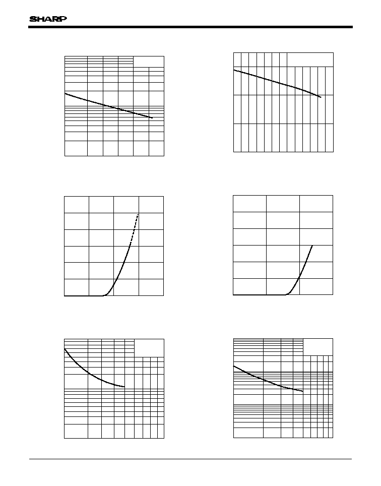
PR26MF11NSZ Series/PR36MF11NSZ Series
Fig.14 ON-state Current vs. ON-state Voltage
(PR26MF21NSZ/PR36MF21NSZ)
Fig.11 Relative Holding Current vs. Ambient Temperature
(PR26MF21NSZ/PR36MF21NSZ)
Fig.12 Zero-cross Voltage vs. Ambient Temperature
(PR26MF21NSZ/PR36MF21NSZ)
0
0.2
0.4
0.6
0.8
1
1.2
0
0.5
1
1.5
ON-state current I
T
(A)
ON-state voltage V
T
(V)
I
F
=
20mA
T
a
=
25�C
10
10
2
10
3
-
30
0
20
40
60
80
100
Relative holding current I
H
(t
�
C) / I
H
(25
�
C)
�
100%
Ambient temperature T
a
(�C)
V
D
=
6V
0
10
5
15
-
30
0
-
20
-
10
20
40
60
80
100
10
30
50
70
90
Zero-cross voltage V
OX
(V)
Ambient temperature T
a
(�C)
R load, I
F
=
15mA
0
0.2
0.4
0.6
0.8
1
1.2
0
0.5
1
1.5
2
ON-state current I
T
(A)
ON-state voltage V
T
(V)
I
F
=
20mA
T
a
=
25�C
1 000
10
100
146.5
1
100
V
D
=
6V
R
L
=100
T
a
=
25�C
10
Forward current I
F
(mA)
Turn-on time t
ON
(
�
s)
Fig.13
ON-state Current vs. ON-state Voltage
(PR26MF11NSZ/PR36MF11NSZ)
Fig.15
Turn-on Time vs. Forward Current
(PR26MF11NSZ)
Fig.16
Turn-on Time vs. Forward Current
(PR36MF11NSZ)
100
10
1
100
V
D
=
6V
R
L
=100
T
a
=
25�C
10
20
30
40
50
Forward current I
F
(mA)
Turn-on time t
ON
(
�
s)
PR26MF11NSZ Series/PR36MF11NSZ Series
Fig.17 Turn-on Time vs. Forward Current (Typical Value)
(PR26MF21NSZ/PR36MF21NSZ)
100
10
1
100
V
D
=
6V
R
L
=100
T
a
=
25�C
10
Forward current I
F
(mA)
Turn-on time t
ON
(
�
s)

115
Application Circuits
NOTICE
qThe circuit application examples in this publication are provided to explain representative applications of
SHARP devices and are not intended to guarantee any circuit design or license any intellectual property
rights. SHARP takes no responsibility for any problems related to any intellectual property right of a
third party resulting from the use of SHARP's devices.
qContact SHARP in order to obtain the latest device specification sheets before using any SHARP device.
SHARP reserves the right to make changes in the specifications, characteristics, data, materials,
structure, and other contents described herein at any time without notice in order to improve design or
reliability. Manufacturing locations are also subject to change without notice.
qObserve the following points when using any devices in this publication. SHARP takes no responsibility
for damage caused by improper use of the devices which does not meet the conditions and absolute
maximum ratings to be used specified in the relevant specification sheet nor meet the following
conditions:
(i) The devices in this publication are designed for use in general electronic equipment designs such as:
--- Personal computers
--- Office automation equipment
--- Telecommunication equipment [terminal]
--- Test and measurement equipment
--- Industrial control
--- Audio visual equipment
--- Consumer electronics
(ii)Measures such as fail-safe function and redundant design should be taken to ensure reliability and
safety when SHARP devices are used for or in connection with equipment that requires higher
reliability such as:
--- Transportation control and safety equipment (i.e., aircraft, trains, automobiles, etc.)
--- Traffic signals
--- Gas leakage sensor breakers
--- Alarm equipment
--- Various safety devices, etc.
(iii)SHARP devices shall not be used for or in connection with equipment that requires an extremely
high level of reliability and safety such as:
--- Space applications
--- Telecommunication equipment [trunk lines]
--- Nuclear power control equipment
--- Medical and other life support equipment (e.g., scuba).
qContact a SHARP representative in advance when intending to use SHARP devices for any "specific"
applications other than those recommended by SHARP or when it is unclear which category mentioned
above controls the intended use.
qIf the SHARP devices listed in this publication fall within the scope of strategic products described in the
Foreign Exchange and Foreign Trade Control Law of Japan, it is necessary to obtain approval to export
such SHARP devices.
qThis publication is the proprietary product of SHARP and is copyrighted, with all rights reserved. Under
the copyright laws, no part of this publication may be reproduced or transmitted in any form or by any
means, electronic or mechanical, for any purpose, in whole or in part, without the express written
permission of SHARP. Express written permission is also required before any use of this publication
may be made by a third party.
qContact and consult with a SHARP representative if there are any questions about the contents of this
publication.