
NPN Silicon RF Transistor
BFQ 72
ESD: Electrostatic discharge sensitive device, observe handling precautions!
Maximum Ratings
Type
Ordering Code
(tape and reel)
Marking
Package
1)
Pin Configuration
BFQ 72
Q62702-F776
72
Cerec-X
1
2
3
B
E
C
4
E
Parameter
Symbol
Values
Unit
Collector-emitter voltage
V
CE0
15
V
Emitter-base voltage
V
EB0
2.5
Collector current
I
C
50
mA
Collector-base voltage
V
CB0
20
Base current
I
B
10
Junction temperature
T
j
175
�C
Ambient temperature range
T
A
� 65 ... + 175
Total power dissipation,
T
S
112 �C
3)
P
tot
350
mW
Storage temperature range
T
stg
� 65 ... + 175
Thermal Resistance
Junction - ambient
2)
R
th JA
260
K/W
Junction - soldering point
3)
R
th JS
180
Collector-emitter voltage,
V
BE
= 0
V
CES
20
1)
For detailed dimensions see chapter Package Outlines.
2)
Package mounted on alumina 15 mm
�
16.7 mm
�
0.7 mm.
3)
T
S
is measured on the collector lead at the soldering point to the pcb.
q
For low-distortion broadband amplifiers up to 2 GHz
at collector currents from 10 mA to 30 mA.
q
Hermetically sealed ceramic package.
q
HiRel/Mil screening available.
q
CECC-type available: CECC 50002/263.

Electrical Characteristics
at
T
A
= 25 �C, unless otherwise specified.
Unit
Values
Parameter
Symbol
min.
typ.
max.
DC Characteristics
V
Collector-emitter breakdown voltage
I
C
= 1 mA,
I
B
= 0
V
(BR)CE0
15
�
�
�
A
Emitter-base cutoff current
V
EB
= 2 V,
I
C
= 0
I
EB0
�
�
10
�
DC current gain
I
C
= 25 mA,
V
CE
= 5 V
I
C
= 50 mA,
V
CE
= 5 V
h
FE
40
40
90
�
200
�
nA
Collector-base cutoff current
V
CB
= 10 V,
I
E
= 0
I
CB0
�
�
50
V
Collector-emitter saturation voltage
I
C
= 50 mA,
I
B
= 5 mA
V
CEsat
�
0.15
0.4
Base-emitter voltage
I
C
= 25 mA,
V
CE
= 5 V
V
BE
�
0.78
�
�
A
Collector-emitter cutoff current
V
CE
= 20 V,
V
BE
= 0
I
CES
�
�
10
BFQ 72

Electrical Characteristics
at
T
A
= 25 �C, unless otherwise specified.
AC Characteristics
Unit
Values
Parameter
Symbol
min.
typ.
max.
Power gain
I
C
= 25 mA,
V
CE
= 8 V,
f
= 800 MHz,
Z
S
=
Z
Sopt
,
Z
L
=
Z
Lopt
G
pe
�
18
�
GHz
Transition frequency
I
C
= 25 mA,
V
CE
= 5 V,
f
= 200 MHz
I
C
= 50 mA,
V
CE
= 5 V,
f
= 200 MHz
f
T
�
�
5.1
4.7
�
�
Collector-emitter capacitance
V
CE
= 10 V,
V
BE
=
v
be
= 0,
f
= 1 MHz
C
ce
�
0.4
�
Output capacitance
V
CE
= 10 V,
V
BE
=
v
be
= 0,
f
= 1 MHz
C
obs
�
0.95
1.5
dB
Noise figure
I
C
= 10 mA,
V
CE
= 8 V,
f
= 10 MHz,
Z
S
= 75
I
C
= 10 mA,
V
CE
= 8 V,
f
= 800 MHz,
Z
S
= 50
F
�
�
1.7
2.5
�
�
pF
Collector-base capacitance
V
CB
= 10 V,
V
BE
=
v
be
= 0,
f
= 1 MHz
C
cb
�
0.55
0.7
Input capacitance
V
EB
= 0.5 V,
I
C
=
i
c
= 0,
f
= 1 MHz
C
ibo
�
2.1
�
Transducer gain
I
C
= 25 mA,
V
CE
= 8 V,
f
= 1 GHz,
Z
0
= 50
I
S
21e
I
2
�
12.5
�
mV
Linear output voltage
two-tone intermodulation test
I
C
= 25 mA,
V
CE
= 8 V,
d
IM
= 60 dB
f
1
= 806 MHz,
f
2
= 810 MHz,
Z
S
=
Z
L
= 50
V
o1
=
V
o2
�
240
�
dBm
Third order intercept point
I
C
= 25 mA,
V
CE
= 8 V,
f
= 800 MHz
IP
3
�
30.5
�
BFQ 72

Total power dissipation
P
tot
=
f
(
T
A
*;
T
S
)
*Package mounted on alumina
Collector-base capacitance
C
cb
=
f
(
V
CB
)
V
BE
=
v
be
= 0,
f
= 1 MHz
Transition frequency
f
T
=
f
(
I
C
)
V
CE
= 5 V,
f
= 200 MHz
BFQ 72

Noise figure
F
=
f
(
Z
S
)
V
CE
= 8 V,
f
= 10 MHz
Common Emitter Noise Parameters
I
C
= 2 mA,
V
CE
= 8 V,
Z
0
= 50
I
C
= 10 mA,
V
CE
= 8 V,
Z
0
= 50
0.01
1.0
�
(
Z
S
= 150
)
�
�
1.6
�
f
opt
GHz
dB
dB
MAG
ANG
�
dB
dB
F
min
G
p
(
F
min
)
R
N
N
F
50
G
p
(
F
50
)
0.01
0.8
1.5
2.3
�
14.7
(
Z
S
= 90
)
99.5
�
16.5
�
0.31
1.7
2.45
�
14
0.26
BFQ 72

Circles of constant noise figure
F
=
f
(
Z
S
)
in
Z
S
-plane,
I
C
= 10 mA,
V
CE
= 8 V,
f
= 800 MHz
Noise figure
F
=
f
(
I
C
)
Power gain
G
=
f
(
I
C
)
V
CE
= 8 V,
f
= 800 MHz,
Z
Lopt
(
G
)
BFQ 72

Common Emitter Power Gain
Power gain
G
ms
,
S
21e
2
=
f
(
I
C
)
V
CE
= 8 V,
f
= 200 MHz,
Z
0
= 50
Power gain
G
ma
,
S
21e
2
=
f
(
I
C
)
V
CE
= 8 V,
f
= 800 MHz,
Z
0
= 50
Power gain
G
ma
,
G
ms
,
S
21e
2
=
f
(
I
C
)
V
CE
= 8 V,
f
= 500 MHz,
Z
0
= 50
Power gain
G
ma
,
S
21e
2
=
f
(
I
C
)
V
CE
= 8 V,
f
= 1.5 GHz,
Z
0
= 50
BFQ 72

Power gain
G
ma
,
G
ms
,
S
21e
2
=
f
(
f
)
I
C
= 10 mA,
V
CE
= 8 V,
Z
0
= 50
Power gain
G
ma
,
G
ms
,
S
21e
2
=
f
(
f
)
I
C
= 40 mA,
V
CE
= 8 V,
Z
0
= 50
Power gain
G
ma
,
G
ms
,
S
21e
2
=
f
(
f
)
I
C
= 25 mA,
V
CE
= 8 V,
Z
0
= 50
BFQ 72
Common Emitter S Parameters
f
S
11
S
21
S
12
S
22
GHz
MAG
ANG
MAG
ANG
MAG
ANG
MAG
ANG
0.1
0.2
0.3
0.4
0.6
0.8
1.0
1.2
1.5
1.8
2.0
2.5
3.0
0.62
0.57
0.56
0.57
0.57
0.58
0.58
0.59
0.59
0.61
0.63
0.64
0.67
� 78
� 121
� 142
� 155
� 169
� 179
174
167
159
153
149
138
128
26.97
17.54
12.39
9.59
6.47
4.86
3.89
3.28
2.64
2.20
1.99
1.63
1.38
137
114
102
94
84
76
69
63
54
46
41
28
16
0.023
0.032
0.039
0.043
0.053
0.064
0.075
0.086
0.102
0.119
0.128
0.153
0.177
59
47
44
45
48
50
50
50
48
46
44
40
34
0.76
0.51
0.38
0.31
0.24
0.21
0.19
0.18
0.17
0.17
0.17
0.17
0.19
� 34
� 50
� 55
� 56
� 57
� 59
� 60
� 63
� 67
� 75
� 82
� 100
� 119
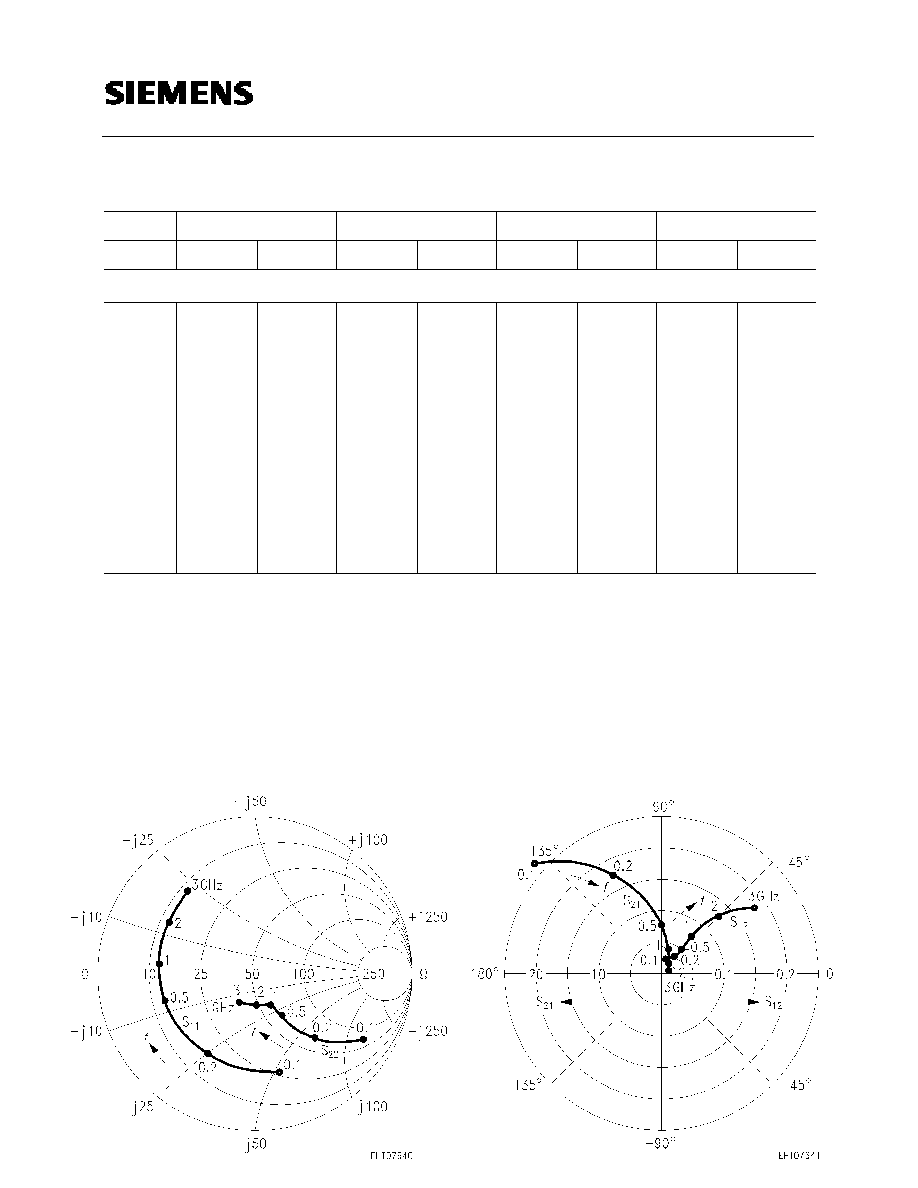
I
C
= 15 mA,
V
CE
= 5 V,
Z
0
= 50
S
11
,
S
22
=
f
(
f
)
I
C
= 15 mA,
V
CE
= 5 V,
Z
0
= 50
S
12
,
S
21
=
f
(
f
)
I
C
= 15 mA,
V
CE
= 5 V,
Z
0
= 50
BFQ 72

S
11
,
S
22
=
f
(
f
)
I
C
= 25 mA,
V
CE
= 5 V,
Z
0
= 50
S
12
,
S
21
=
f
(
f
)
I
C
= 25 mA,
V
CE
= 5 V,
Z
0
= 50
Common Emitter S Parameters (continued)
f
S
11
S
21
S
12
S
22
GHz
MAG
ANG
MAG
ANG
MAG
ANG
MAG
ANG
0.1
0.2
0.3
0.4
0.6
0.8
1.0
1.2
1.5
1.8
2.0
2.5
3.0
0.54
0.55
0.55
0.57
0.57
0.58
0.59
0.60
0.60
0.61
0.63
0.65
0.68
� 99
� 137
� 154
� 164
� 176
176
170
165
157
151
147
137
127
31.95
19.18
13.20
10.09
6.76
5.06
4.04
3.40
2.74
2.28
2.06
1.68
1.42
130
108
98
91
82
74
68
62
54
46
41
29
17
0.018
0.027
0.032
0.037
0.049
0.061
0.072
0.084
0.101
0.118
0.127
0.153
0.177
57
48
49
52
55
56
55
55
52
49
47
42
36
0.66
0.42
0.30
0.24
0.19
0.17
0.15
0.14
0.14
0.14
0.14
0.14
0.17
� 41
� 55
� 59
� 60
� 60
� 61
� 63
� 66
� 70
� 79
� 87
� 106
� 126
I
C
= 25 mA,
V
CE
= 5 V,
Z
0
= 50
BFQ 72

Common Emitter S Parameters (continued)
f
S
11
S
21
S
12
S
22
GHz
MAG
ANG
MAG
ANG
MAG
ANG
MAG
ANG
0.1
0.2
0.3
0.4
0.6
0.8
1.0
1.2
1.5
1.8
2.0
2.5
3.0
0.51
0.55
0.55
0.58
0.59
0.60
0.61
0.62
0.62
0.64
0.66
0.67
0.70
� 126
� 154
� 166
� 173
178
172
167
162
155
149
145
136
126
34.20
18.99
12.81
9.72
6.47
4.84
3.86
3.25
2.62
2.18
1.97
1.61
1.37
121
103
94
88
80
73
67
62
53
45
41
29
18
0.014
0.021
0.026
0.032
0.045
0.057
0.069
0.080
0.097
0.114
0.123
0.149
0.174
54
53
57
59
62
61
60
59
56
53
51
46
40
0.55
0.33
0.25
0.21
0.18
0.17
0.16
0.15
0.15
0.15
0.15
0.15
0.17
� 46
� 52
� 52
� 51
� 50
� 52
� 55
� 59
� 65
� 74
� 83
� 104
� 125
I
C
= 50 mA,
V
CE
= 5 V,
Z
0
= 50
S
11
,
S
22
=
f
(
f
)
I
C
= 50 mA,
V
CE
= 5 V,
Z
0
= 50
S
12
,
S
21
=
f
(
f
)
I
C
= 50 mA,
V
CE
= 5 V,
Z
0
= 50
BFQ 72

Common Emitter S Parameters (continued)
f
S
11
S
21
S
12
S
22
GHz
MAG
ANG
MAG
ANG
MAG
ANG
MAG
ANG
0.1
0.2
0.3
0.4
0.6
0.8
1.0
1.2
1.5
1.8
2.0
2.5
3.0
0.69
0.61
0.57
0.56
0.55
0.55
0.56
0.56
0.57
0.58
0.60
0.62
0.65
� 59
� 100
� 124
� 140
� 159
� 171
� 179
173
164
157
152
141
131
22.59
16.18
11.90
9.39
6.42
4.86
3.90
3.29
2.66
2.21
2.00
1.64
1.39
145
121
108
99
87
78
71
65
55
46
41
28
17
0.023
0.036
0.042
0.046
0.055
0.064
0.073
0.082
0.096
0.110
0.119
0.141
0.162
63
49
44
43
44
45
46
46
45
44
42
39
35
0.85
0.64
0.51
0.43
0.36
0.33
0.31
0.30
0.29
0.29
0.28
0.28
0.28
� 24
� 37
� 41
� 43
� 43
� 44
� 46
� 48
� 52
� 59
� 64
� 78
� 95
I
C
= 10 mA,
V
CE
= 8 V,
Z
0
= 50
S
11
,
S
22
=
f
(
f
)
I
C
= 10 mA,
V
CE
= 8 V,
Z
0
= 50
S
12
,
S
21
=
f
(
f
)
I
C
= 10 mA,
V
CE
= 8 V,
Z
0
= 50
BFQ 72

Common Emitter S Parameters (continued)
f
S
11
S
21
S
12
S
22
GHz
MAG
ANG
MAG
ANG
MAG
ANG
MAG
ANG
0.1
0.2
0.3
0.4
0.6
0.8
1.0
1.2
1.5
1.8
2.0
2.5
3.0
0.55
0.53
0.52
0.54
0.54
0.55
0.56
0.56
0.57
0.59
0.61
0.62
0.66
� 90
� 131
� 150
� 160
� 172
179
172
167
159
153
149
139
129
32.99
20.17
13.96
10.71
7.17
5.38
4.29
3.62
2.91
2.42
2.18
1.78
1.51
132
110
99
92
83
75
69
63
54
47
42
30
18
0.017
0.024
0.030
0.035
0.046
0.057
0.067
0.078
0.094
0.109
0.119
0.142
0.165
56
50
50
53
56
57
56
55
53
50
48
44
39
0.71
0.46
0.36
0.30
0.26
0.24
0.23
0.22
0.22
0.22
0.21
0.21
0.22
� 35
� 44
� 45
� 44
� 43
� 43
� 45
� 47
� 51
� 59
� 65
� 80
� 98
I
C
= 25 mA,
V
CE
= 8 V,
Z
0
= 50
S
11
,
S
22
=
f
(
f
)
I
C
= 25 mA,
V
CE
= 8 V,
Z
0
= 50
S
12
,
S
21
=
f
(
f
)
I
C
= 25 mA,
V
CE
= 8 V,
Z
0
= 50
BFQ 72

Common Emitter S Parameters (continued)
f
S
11
S
21
S
12
S
22
GHz
MAG
ANG
MAG
ANG
MAG
ANG
MAG
ANG
0.1
0.2
0.3
0.4
0.6
0.8
1.0
1.2
1.5
1.8
2.0
2.5
3.0
0.51
0.52
0.53
0.54
0.55
0.56
0.57
0.58
0.59
0.60
0.62
0.64
0.67
� 108
� 144
� 159
� 167
� 177
176
170
165
157
152
148
138
128
35.70
20.53
13.96
10.64
7.10
5.32
4.24
3.57
2.87
2.39
2.16
1.77
1.50
126
105
96
90
81
74
68
63
54
46
42
29
18
0.016
0.021
0.027
0.032
0.043
0.054
0.066
0.076
0.092
0.107
0.116
0.140
0.163
57
52
55
57
60
60
59
58
56
52
51
46
41
0.64
0.41
0.32
0.28
0.25
0.24
0.23
0.22
0.22
0.22
0.21
0.21
0.22
� 37
� 42
� 41
� 39
� 38
� 39
� 41
� 44
� 49
� 57
� 63
� 79
� 98
I
C
= 40 mA,
V
CE
= 8 V,
Z
0
= 50
S
11
,
S
22
=
f
(
f
)
I
C
= 40 mA,
V
CE
= 8 V,
Z
0
= 50
S
12
,
S
21
=
f
(
f
)
I
C
= 40 mA,
V
CE
= 8 V,
Z
0
= 50
BFQ 72