
Functional Description
The NMOS device SDA 9290-5 is a picture processor and belongs to a family of devices forming
an extended third-generation digital TV signal-processing system for enhanced picture quality with
special functions (Featurebox). Besides the Picture Processor (PP) that is described here, the
system consists of a field memory (at least three triple-port, 1-Mbit generation TV Sequential-
Access Memory devices (SDA 9251 X), a Memory Sync Controller (MSC SDA 9220-5) and a Video
D/A converter (SDA 9094-5). A block diagram of the Featurebox is shown in figure 1.
The Picture Processor SDA 9290-5 is a follow-on development of the Picture Processor SDA 9090
from the second-generation Featurebox and permits further picture improvement by reducing the
video noise and cross-color interference. The SDA 9290-5 can be set independently at the picture-
signal input and output via the two pins FSBQ/FSI to the 4:1:1 and 4:2:2 formats. A 4:1:1
Featurebox (3 TV-SAMs) can therefore be operated with 4:2:2 input signals as well.
Type
Ordering Code
Package
SDA 9290-5
Q67100-H5088
P-LCC-68-1 (SMD)
Picture Processor
Preliminary Data
NMOS IC
SDA 9290-5
P-LCC-68-1
Features
q
Noise and cross color reduction by field - or frame
recursive filtering
q
3 adjustments: 4-dB-, 7-dB- or 12-dB reduction
q
Automatic adaption to signal quality during vertical
blanking
q
Pixel adaptive movement detection
q
Split screen modes for demonstration purposes
q
Multi-picture facilities
q
Picture decimation using vertical filtering
q
8 programmable grey levels for framing
q
4:1:1 and 4:2:2 (Y:U:V) compatibility
q
8-bit word size for all components
Semiconductor Group
259
01.94

SDA 9290-5
Semiconductor Group
260
The necessary decimation and interpolation operations are activated automatically when the format
is set. Together with a corresponding Memory Sync Controller (SDA 9220) it enables functions like
multi-picture, tuner scanning, picture-in-still and still-in-picture. The different modes can be
activated by a microcontroller on the
I
2
C Bus interface (slave receiver). The
I
2
C Bus address for
accessing the device is
Circuit Description
The core of the picture processor (see block diagram) is formed of the Image-lmproving Processor
(IIP) and the Multi-Picture Processor (MPP). The IIP is responsible for noise and cross-color
reduction, while the MPP together with the new Memory Sync Controller implements the functions
multi-picture, tuner scanning, picture-in-still and still-in-picture.
Image-lmproving Processor
The signal inputs Yl0-YI7 and UVI0-UVI7 and the back-channel signal inputs YB0-YB7 and UVB0-
UVB7 picture data with 12 bits in quasi-parallel format (4:1:1) and with 16 bits in parallel format
(4:2:2). The clock rate for both signals is 13.5 MHz. For signal processing in the IIP and MPP the
chrominance bit levels have to be separated in the case of the quasi parallel format by
demultiplexers DEMUXS and DEMUXR, these being largely identical in design.
A reduction in video noise is achieved by correlating the picture contents of two successive fields,
the non-correlated components (noise) being attenuated by the digital filter. To achieve this, the
instantaneous digital picture signal on the outputs of the demultiplexer DEMUXS and the picture
signal delayed by a field interval on the outputs of the back-channel demultiplexer DEMUXR are fed
to the IIP and combined.
The signal-to-noise ratio (
S/N
) unit detects the noise components of the input signals and the
movement detector uses this information to select an appropriate set of parameters with filter
coefficients and thresholds for the comparators. For this purpose the luminance signal is assigned
to one of three classes according to its
S/N
ratio, with each class defining a different degree of
maximum noise reduction. The limits between the middle class and the upper and lower classes
can be programmed by the I
2
C Bus registers R1 and R2 with the values for the thresholds SU and
SL. When the picture signals come from a video cassette recorder, the adaptation on the
S/N
ratio
of the input signal should be disabled by
I
2
L Bus register R0, VCR bit D2.
Measurement of the signal-to-noise ratio in the automatic mode has been advanced from line 7 to
line 6 in order to avoid conflicts with future text and data services.
The degree of noise reduction for the luminance and chrominance signals can be varied between
0 dB and 12 dB by selecting the appropriate filter coefficients.
A picture signal with reduced noise and cross-color appears on the output of the IIP for further
processing. The signal will be forwarded via blocks MUXI and MUXO to the picture memories
through the outputs (YQ0-YQ7 and UVQO-UVQ7 respectively).
The coefficients of the selected class are controlled by the movement detector as a function of
pixels to prevent artifacts (loss of focus) in moving parts of the picture.
0
0
1
0
1
0
1
0

SDA 9290-5
Semiconductor Group
261
Multi-Picture Processor
Signals are processed in the 4:1:1 format. The vertical-decimation line memory now operates with
208 (formerly 216) pixels per line to adapt the 1/9th picture format to the new picture memory with
TV-SAMs. Gray frame generation is similarly affected by this change in pixel value.
The signal processing in the decimation filter of the MPP reduces the picture to approximately 1/9th
of its original size. This produces a basis for new features, the full implementation of which calls for
a matching MSC (SDA 9220).
Figure 5 shows how the screen is divided up. The following modes can be implemented with the
MPP:
1. Multi-Picture (automatic)
Fields are extracted from a sequence of movements at fixed intervals, reduced and reproduced
on the screen as a sequence of stills. At one position it is possible to show a moving picture.
2. Multi-Picture (manual)
This differs from the above in that the viewer can determine at the push of a button what phases
of movement are to be stored.
3. Multi-Picture (tuner scanning)
The pictures of the sequence of stills are derived from the different TV channels and give an
overview of the programs on offer. In this mode the picture memory is operated with a crystal-
controlled clock to ensure that the picture remains stable when switching from one channel to
another.
4. Still-in-Picture
A field is extracted from the on-going program, reduced and inserted as a still in the master
channel.
5. Picture-in-Still
The on-going program is inserted as a reduced-size moving picture in a still.
The framing block that follows the decimation filter in the MPP permits frames to be inserted in order
to border the reduced-size pictures on the screen. The brightness of the framing can be varied in
eight steps by the
I
2
C Bus.
The format conversion produced in the demultiplexers for signal processing in the IIP and MPP is
reversed again in the multiplexer MUXO. The picture signal appears again in quasi-parallel format
or parallel format on the output of the MUXO block. The inputs of the TV-SAMs are directly driven
by the sixteen outputs YQ0-YQ7 and UVQ0-UVQ7.

SDA 9290-5
Semiconductor Group
262
I
2
C Bus Interface
An
I
2
C Bus interface configured as a "slave receiver" is used for programming the different functions
and modes of the picture processor. Via this interface up to four registers can be written according
to the following transfer protocol for controlling the operation mode:
S: Start condition
A: Acknowledge
P: Stop condition
Slave address: 0 0 1 0 1 0 1
(Note: There is a general description of the
I
2
C Bus in the Siemens publication "
I
2
C Bus Technical
Description".)
After every data byte that is transmitted the internal register address (subaddress) is automatically
incremented to the next register so that, if necessary, several registers can be loaded with one
I
2
C
Bus telegram.
In the multi-picture mode the operating mode transmitted on the
I
2
C Bus is switched within the
vertical blanking interval, i.e. during the high phase of signal VS1, if the Memory Sync Controller
(MSC) activates the DREQ line during this period.
It should be noted that the new operating mode has always to be transmitted to the picture
processor first and immediately afterwards to the MSC on the
I
2
C Bus at an interval not longer than
30 ms.
This is the only way to ensure interference-free synchronization of the picture processor and the
MSC. The four
I
2
C Bus registers are described below in more detail. The values marked "*D" in the
right-hand margin are set by an internally generated reset signal (default values) when the
operating voltage is applied.
Register Sub-
address
1)
Data Byte
D7
D6
D5
D4
D3
D2
D1
D0
R0
00
B1
B0
FR
0
SS
VCR
NR
SUV8
R1
01
YF5
YF4
YF3
SL4
SL3
SL2
SL1
SL0
R2
02
0
0
0
SU4
SU3
SU2
SU1
SU0
R3
03
SNTEN SNT1
SNT0
KTEN
KT3
KT2
KT1
KT0
S
0 A
A
A
A P
Slave Address
Sub Address
Data Byte

SDA 9290-5
Semiconductor Group
263
Specialities:
Split Screen Display
For demonstration purposes the noise reduction can be disabled for half of the picture by means of
I
2
C Bus register R0, bit D3. In this way a direct comparison is possible between a noise-reduced
(filtered) and an unfiltered picture.
Register R0: This control register sets the operating mode of the picture processor.
Bits D7, D6:
Mode
B1
B0
Normal
0
0
*D
Multi-picture (MP)
0
1
Still-in-picture (SIP)
1
0
Picture-in still (PIS)
1
1
Bit D5:
MPP: Narrow Frame
FR
Without narrow frame
0
With narrow frame
1
Bit D4:
No function; default 0
Bit D3:
Display Mode
SS
Full screen
0
*D
Split screen
1
Bit D2:
Control of SNR adaptation
VCR
TV mode
0
*D
VCR mode
1
Bit D1:
Noise reduction ON/OFF
NR
Noise reduction OFF
0
*D
Noise reduction ON
1
Bit D0:
Word width input
SUV8
7 bits
0
8 bits
1

SDA 9290-5
Semiconductor Group
264
Register R1: This control register sets the frame luminance for multi-picture and the threshold SL
for S/N adaptation.
Bits D7-D5:
Frame Luminance YF
YF5
YF4
YF3
0
black
0
0
0
*D
:
:
:
:
:
:
7
white
:
:
:
1
:
:
:
1
:
:
:
1
Bits D4-D0:
Threshold SL
(S/N adaptation)
SL4
SL3
SL2
SL1
SL0
0
0
0
0
0
0
:
:
:
:
:
:
:
:
:
:
:
:
4
0
0
1
0
0
*D
:
:
:
:
:
:
:
:
:
:
:
:
31
1
1
1
1
Register R2: This control register sets the threshold SU for S/N adaptation.
Bits D7-D5:
No function; default 0
Bits D4-D0:
Threshold SL
(S/N adaptation)
SU4
SU3
SU2
SU1
SU0
0
0
0
0
0
0
:
:
:
:
:
:
:
:
:
:
:
:
16
1
0
0
0
0
*D
:
:
:
:
:
:
:
:
:
:
:
:
31
1
1
1
1
1

SDA 9290-5
Semiconductor Group
265
Note: X is ignored.
*D = Default values after reset.
Register R3: This register is for testing. certain S/N classes and filter coefficients for the motion
detector can be firmly set.
Bits D7-D5:
S/N Class
SNTEN
SNT1
SNT0
Automatic adaptation
0
X
X
*D
Class 0
1
0
0
Class 1
1
0
1
Class 2
1
1
0
Bits D4-D0:
Filter Coefficient
KTEN
KT3
KT2
KT1
KT0
Motion detector ON
0
X
X
X
X
*D
K = 1
1
0
0
0
0
K = 3/4
1
0
0
0
1
K = 5/8
1
0
0
1
0
K = 9/16
1
0
0
1
1
K = 3/4
1
0
1
0
0
K = 1/2
1
0
1
0
1
K = 3/8
1
0
1
1
0
K = 5/16
1
0
1
1
1
K = 5/8
1
1
0
0
0
K = 3/8
1
1
0
0
1
K = 1/4
1
1
0
1
0
K = 3/16
1
1
0
1
1
K = 9/16
1
1
1
0
0
K = 5/16
1
1
1
0
1
K = 3/16
1
1
1
1
0
K = 1/8
1
1
1
1
1

SDA 9290-5
Semiconductor Group
266
Block Diagram

SDA 9290-5
Semiconductor Group
267
Pin Configuration
(top view)
SDA 9290-5
Semiconductor Group
268
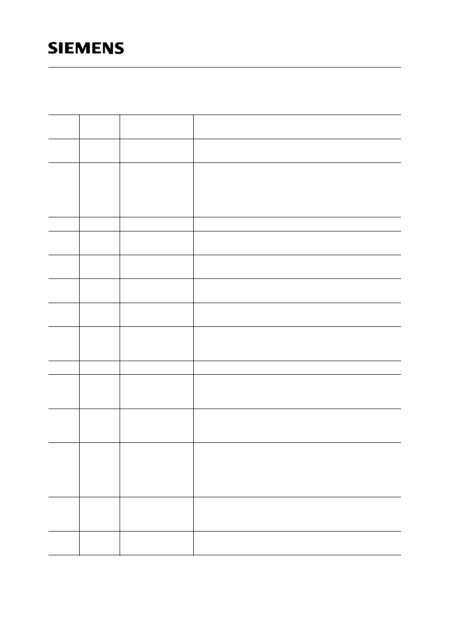
Pin Definitions and Functions
Pin
No.
Symbol
Function
Description
1
V
DD
Positive supply
voltage (+ 5 V)
Positive supply voltage (+ 5 V)
2-9
UVQ7 ...
UVQ0
Data outputs
Push-pull outputs for directly driving the TV-SAM
chrominance inputs:
8 bits for 4:2:2 format;
4 bits for 4:1:1 format;
[UVQ0 ... UVQ3 only valid for 4:2:2 format]
10
V
SS
Ground
Ground (0 V)
11-18
UVB0 ...
UVB7
Back-channel data
outputs
Back-channel inputs for chrominance data from TV-SAM
19-26
YB0 ...
YB7
Back- channel
data inputs
Back-channel inputs for luminance data from TV-SAM
27-34
UVI0 ...
UVI7
Data inputs
Data inputs for chrominance data accept the dig. YUV
signal
35-42
YI0 ...
YI7
Data inputs
Data inputs for luminance data accept the dig. YUV
signal
43
DREQ
Data request
signal for multi-
picture mode
Data-request input; initiates data transfer in multi-picture
mode and switches mode together with signal VS1
44
V
SS
Ground
Ground (0 V)
45
BLN
Blanking signal
(15.625 kHz)
Input for line-synchronous blanking signal that
determines line blanking interval (active low) and
synchronizes clock and sequence control
46
LLIN
First system clock
(13.5 or 27 MHz)
Input for line-locked system clock, optionally 13.5 MHz or
27 MHz, from which internal timing is derived. Positive
edge indicates validity of input data
47
LLSEL
Selection of
system clock
frequency (LLIN)
Selection of input clock frequency at pin LLIN for
adapting the IC to the system clock. Low level for
27-MHz clock frequency; high level for 13.5-MHz clock
frequency; no switching inactive mode without picture
interference
48
LL3X
Second system
clock (13.5 MHz)
Input for line-locked 13.5-MHz clock that ensured picture
stability in multi-picture mode and is used as output clock
in every mode
49
SCL
I
2
C Bus shift clock
input
I
2
C Bus shift-clock input
SDA 9290-5
Semiconductor Group
269
50
SDA
I
2
C Bus data
input/output
I
2
C Bus data input/output
51
VS1
Vertical sync input
(50 Hz)
Vertical sync input; determines vertical position of TV
picture for 50-Hz or 60-Hz field frequency
52
V
DD
Positive supply
voltage (+ 5 V)
Positive supply voltage (+ 5 V)
53
FSBQ
Selection of output
format
Switching of data output format:
Low level for 4:1:1 format; high level for 4:2:2 format
54
FSI
Selection of input
format
Switching of data input format: Low level for 4:1:1 format;
high level for 4:2:2 format
55
CLKEN
Connect test pin 2
Has to be grounded (0 V) in normal mode
56
SPEN
Connect test pin 2
Has to be grounded (0 V) in normal mode
57-59
N.C.
Reserved
No connections possible or meaningful
60
V
SS
Ground
Ground (0 V)
61-68
YQ7 ...
YQ0
Data outputs
Push-pull outputs for directly driving TV-SAM inputs for
4:1:1 and 4:2:2 modes; (8-bit luminance)
Absolute Maximum Ratings
(all voltages are referred to
V
SS
)
Parameter
Symbol
Limit Values
Unit
Remarks
min.
max.
Ambient temperature
T
A
0
70
�
C
Storage temperature
T
stg
� 40
125
�
C
Total power dissipation
P
tot
2.5
W
Supply voltage
V
DD
� 0.3
6
V
Input/output voltage
V
I/Q
� 0.3
6
V
Thermal resistance system-air
R
th SA
25
K/W
with heat sink
Operating Range
Supply voltage
V
DD
4.5
5.5
V
Supply current
I
DD
450
mA
Ambient temperature
T
A
0
70
�
C
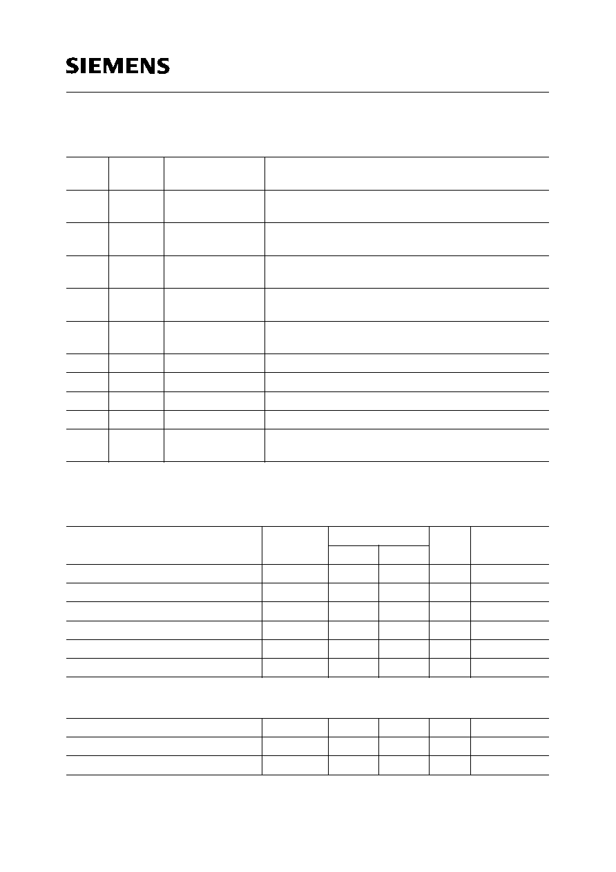
Pin Definitions and Functions (cont'd)
Pin
No.
Symbol
Function
Description

SDA 9290-5
Semiconductor Group
270
Characteristics
(all voltages are referred to
V
SS
)
Parameter
Symbol
Limit Values
Unit
Test Condition
min.
typ.
max.
H-input voltage
1)
V
IH
2.0
5.5
V
L-input voltage
1)
V
IL
0
0.8
V
Input current
1)
I
IR
10
�
A
Input capacitance
1)
(except BLN, LLIN)
C
I
10
pF
Input capacitance
1)
(only BLN, LLIN)
C
I
5
pF
H-input voltage
2)
V
IH
3.0
5.5
V
L-input voltage
2)
V
IL
0
0.8
V
Input capacitance
2)
C
I
10
pF
Input current
2)
I
IM
10
�
A
H-output voltage
3)
V
QH
2.4
V
I
QH
= � 2.0 mA
L-output voltage
3)
V
QL
0.4
V
I
QH
= 3.0 mA
L-output voltage
4)
V
QL
0.4
V
I
QH
= 3.0 mA
Permissible output voltage
4)
V
QM
5.5
V
1)
Input signals UVI0 ... UVI7, YI0 ... YI7, UVB0 ... UVB7, YB0 ... YB7, BLN, LLSEL, FSI, FSBQ, LLIN, LL3X,
DREQ, VS1
2)
Input signals SDA, SCL (refer to figure 3)
3)
Output signals YQ0-YQ7, UVQ0-UVQ7
4)
Output signal SDA (open drain)

SDA 9290-5
Semiconductor Group
271
Input Clock LL3X = 13.5 MHz (refer to figure 3)
Cycle
T
LLL3X
68
74
80
ns
Fall time
t
THL
5
ns
Rise time
t
THL
5
ns
H-pulse width
t
WH
25
ns
L-pulse width
t
WL
25
ns
Change in rel to LLIN
t
SK
0
15
ns
Input Clock LLIN (refer to figure 3)
Cycle
T
LLIN
68
74
80
ns
LLSEL = high
H-pulse width
t
WH
25
ns
LLSEL = high
L-pulse width
t
WL
25
ns
LLSEL = high
Cycle
T
LLIN
35
37
40
ns
LLSEL = low
H-pulse width
t
WH
10
ns
LLSEL = low
L-pulse width
t
WL
10
ns
LLSEL = low
Fall time
t
THL
5
ns
Rise time
t
THL
2
5
ns
Input Clock BLN (refer to figure 2)
Setup time
t
SU
7
ns
LLSEL = low
Hold time
t
IH
6
ns
LLSEL = low
Setup time
t
SU
15
ns
LLSEL = high
Hold time
t
IH
5
ns
LLSEL = high
H-pulse width
t
WH
720
T
LL3X
Cycle, 625 lines
T
BLN
864
T
LL3X
Cycle, 525 lines
T
BLN
858
T
LL3X
Characteristics (cont'd)
(all voltages are referred to
V
SS
)
Parameter
Symbol
Limit Values
Unit
Test Condition
min.
typ.
max.

SDA 9290-5
Semiconductor Group
272
Input Signal VS1
Setup time
t
SU
15
ns
Reference LL3X
Hold time
t
IH
5
ns
Reference LL3X
Cycle, 625 lines
T
VS1
312.5
T
BLN
Cycle, 525 lines
T
VS1
262.5
T
BLN
H-pulse width, 625 lines
t
WH
26.5
T
BLN
L-pulse width, 525 lines
t
WL
16.5
T
BLN
Input Signal DREQ
Setup time
t
SU
15
ns
Reference LL3X
Hold time
t
IH
5
ns
Reference LL3X
H-pulse width
t
WH
1
16
T
LL3X
Input Signal (Data) YI0 ... YI7, UVI0 ... UVI7, YB0 ... YB7, UVB0 ... UVB7 (refer to figure 2)
Setup time
t
SU
15
ns
Reference LL3X
Hold time
t
IH
5
ns
Reference LL3X
Setup time
t
SU
15
ns
Reference LLIN
Hold time
t
IH
5
ns
Reference LLIN
Output Signal (Data) YQ0 ... YQ7, UVQ0 ... UVQ7 (refer to figure 2)
Hold time
t
QH
6
ns
Reference LL3X
Delay time
t
QD
50
ns
Reference LL3X
C
L
= 30 pF
Characteristics (cont'd)
(all voltages are referred to
V
SS
)
Parameter
Symbol
Limit Values
Unit
Test Condition
min.
typ.
max.

SDA 9290-5
Semiconductor Group
273
Figure 1
Application Circuit (simplified)

SDA 9290-5
Semiconductor Group
274
Figure 2
Timing Diagram

SDA 9290-5
Semiconductor Group
275
Figure 3
Timing Diagram

SDA 9290-5
Semiconductor Group
276
Figure 4
Timing for
I
2
C Bus
All values are referred to specified input levels
V
IH
and
V
IL
.
Parameter
Symbol
Limit Values
Unit
min.
max.
Clock frequency
f
SCL
0
100
kHz
Inactive time before start of new transmission
t
BUF
4.7
�
s
Hold time for start condition
(after this time first clock pulse is generated)
t
HD; STA
4.0
�
s
Low clock phase
t
LOW
4.7
�
s
High clock phase
t
HIGH
4.0
�
s
Setup time for data
t
SU; DAT
250
ns
Rise time for SDA and SCL signals
t
TLH
1
�
s
Fall time for SDA and SCL signals
t
THL
300
ns
Setup time for SCL clock in stop condition
t
SU; STO
4.7
�
s

SDA 9290-5
Semiconductor Group
277
Figure 5
Picture Formats for 9-Image Display

SDA 9290-5
Semiconductor Group
278
Y: Luminance Signal
U: Chrominance Signal
V: Chrominance Signal
Figure 6
Assignment of Signal and Pin Names
Format 4:1:1
Y:7-Bit Signal
Y:8-Bit Signal
Picture Processor
Input
Back Channel
Input
Output
Y6
Y7
YI7
YB7
YQ7
Y5
Y6
YI6
YB6
YQ6
Y4
Y5
YI5
YB5
YQ5
Y3
Y4
YI4
YB4
YQ4
Y2
Y3
YI3
YB3
YQ3
Y1
Y2
YI2
YB2
YQ2
Y0
Y1
YI1
YB1
YQ1
�
Y0
YI0
YB0
YQ0
U6 U4 U2 U0
U7 U5 U3 U1
UVI7
UVB7
UVQ7
U5 U3 U1
U6 U4 U2 U0
UVI6
UVB6
UVQ6
V6 V4 V2 V0
V7 V5 V3 V1
UVI5
UVB5
UVQ5
V5 V3 V1
V6 V4 V2 V0
UVI4
UVB4
UVQ4

SDA 9290-5
Semiconductor Group
279
Figure 7
Assignment of Signal and Pin Names
Format 4:2:2
Signal
Picture Processor
Input
Back Channel
Input
Output
Y7
YI7
YB7
YQ7
Y6
YI6
YB6
YQ6
Y5
YI5
YB5
YQ5
Y4
YI4
YB4
YQ4
Y3
YI3
YB3
YQ3
Y2
YI2
YB2
YQ2
Y1
YI1
YB1
YQ1
Y0
YI0
YB0
YQ0
UV7
UVI7
UVB7
UVQ7
UV6
UVI6
UVB6
UVQ6
UV5
UVI5
UVB5
UVQ5
UV4
UVI4
UVB4
UVQ4
UV3
UVI3
UVB3
UVQ3
UV2
UVI2
UVB2
UVQ2
UV1
UVI1
UVB1
UVQ1
UV0
UVI0
UVB0
UVQ0

SDA 9290-5
Semiconductor Group
280
Figure 8
Output Data Delay Times