Document Outline
- ˛ˇ
- ˛ˇ
- ˛ˇ
- ˛ˇ
- ˛ˇ
- ˛ˇ
- ˛ˇ
- ˛ˇ
- ˛ˇ
- ˛ˇ
- ˛ˇ
- ˛ˇ

Rev.1.1
Seiko Instruments Inc.
1
The S-70L01AQS microcomputer incorporates a decoder conforming to CCIR
Radio Paging Decode 1(POCSA Code), a melody generator, an LCD driver and
a timer. Only attaching externally a radio frequency circuit, an LCD panel,
EEPROM for ID purpose and other parts makes it easy to create a numeric
pager.
The circuit without DC/DC converter can also be operated by one battery
because it is operated at min. 0.9V. The circuit configuration reduces radiation
noises and power consumption.
The decoder can support decoding, error correction and data length conversion
like SEIKO decoder IC S-70L41BFT and is provided with several customizing
functions.
A 76.8 kHz quartz crystal oscillator is used to respond to data rates 512, 1200
and 2400 bps
n
n
Features
∑
Low voltage operation:
0.9 V min.
∑
Low current consumption:
10
µ
A typ. at 1. 5 V
∑
Oscillator:
Crystal oscillator (76.8 kHz)
∑
CPU core:
8bit CPU (65C02)
∑
ROM/RAM:
8 k byte ROM/512 byte RAM
∑
Port:
4bit Output,8bit I/O
∑
Timer/counter:
8bit Programmable Timer / Watch Timer
∑
LCD driver configuration:
32 segments x 4 commons
∑
Data rate:
512/1200/2400 bps
∑
Address/Frame:
6 addresses/ 6 frames
∑
2-bit error random correction
∑
Melody generator
n
n
Brief Specifications
Table 1 Brief Specifications
Item
Specifications
Conditions
Operating power supply voltage range
V
DD
= 0.9 to 2.2 V
Fosc = 76.8 KHz
Average current consumption during standby
10
µ
A
V
DD
= 1.5V, Ta = 25
∞
C
Current consumption during HALT mode
6
µ
A
V
DD
= 1.5V, Ta = 25
∞
C
Operating temperature range
-
10 to 55
∞
C
MICROCOMPUTER WITH BUILT-IN PAGING DECODER
S-70L01AQS
NOTICE
∑
Note that the products incorporating SEIKO paging decoder built-in microcomputers may infringe upon
any patent depending upon applications including applied circuits herein, specifications or countries of
destination of the products.
∑
Pay great attention to copyright of melody when you use a melody generator using SEIKO paging
decoder built-in microcomputers.
∑
If the products incorporating SEIKO paging decoder built-in microcomputers may infringe upon any
patent or copyright, Seiko Instruments Inc. shall not be liable for any matters arising out of or in
connection with such patent or copyright infringement.
MICROCOMPITER WITH BUILT-IN PAGING DECODER
S-70L01AQS
2
Seiko Instruments Inc.
n
n
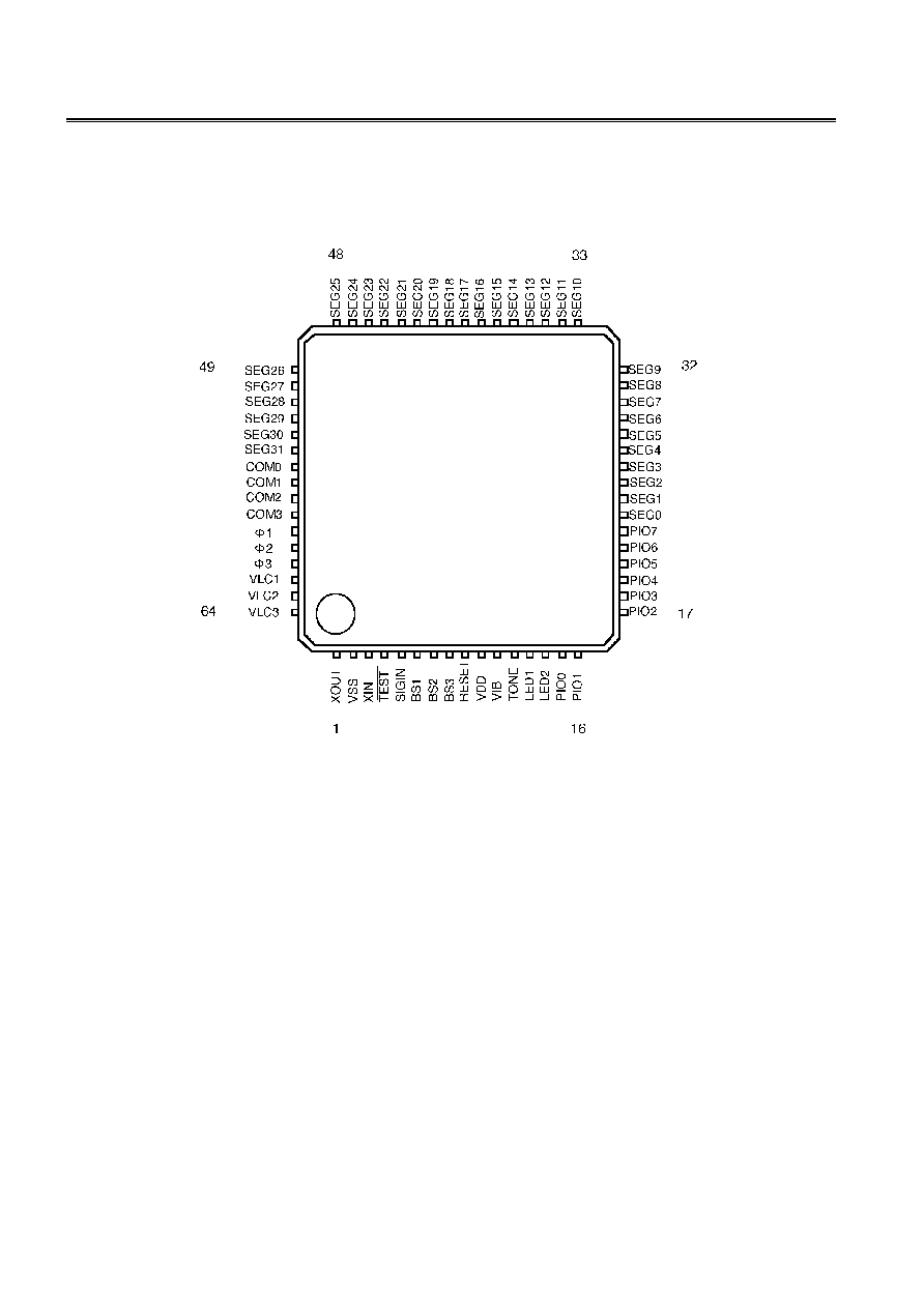
Pin Assignment
Figure 1
MICROCOMPITER WITH BUILT-IN PAGING DECODER
S-70L01AQS
Seiko Instruments Inc.
3
n
n
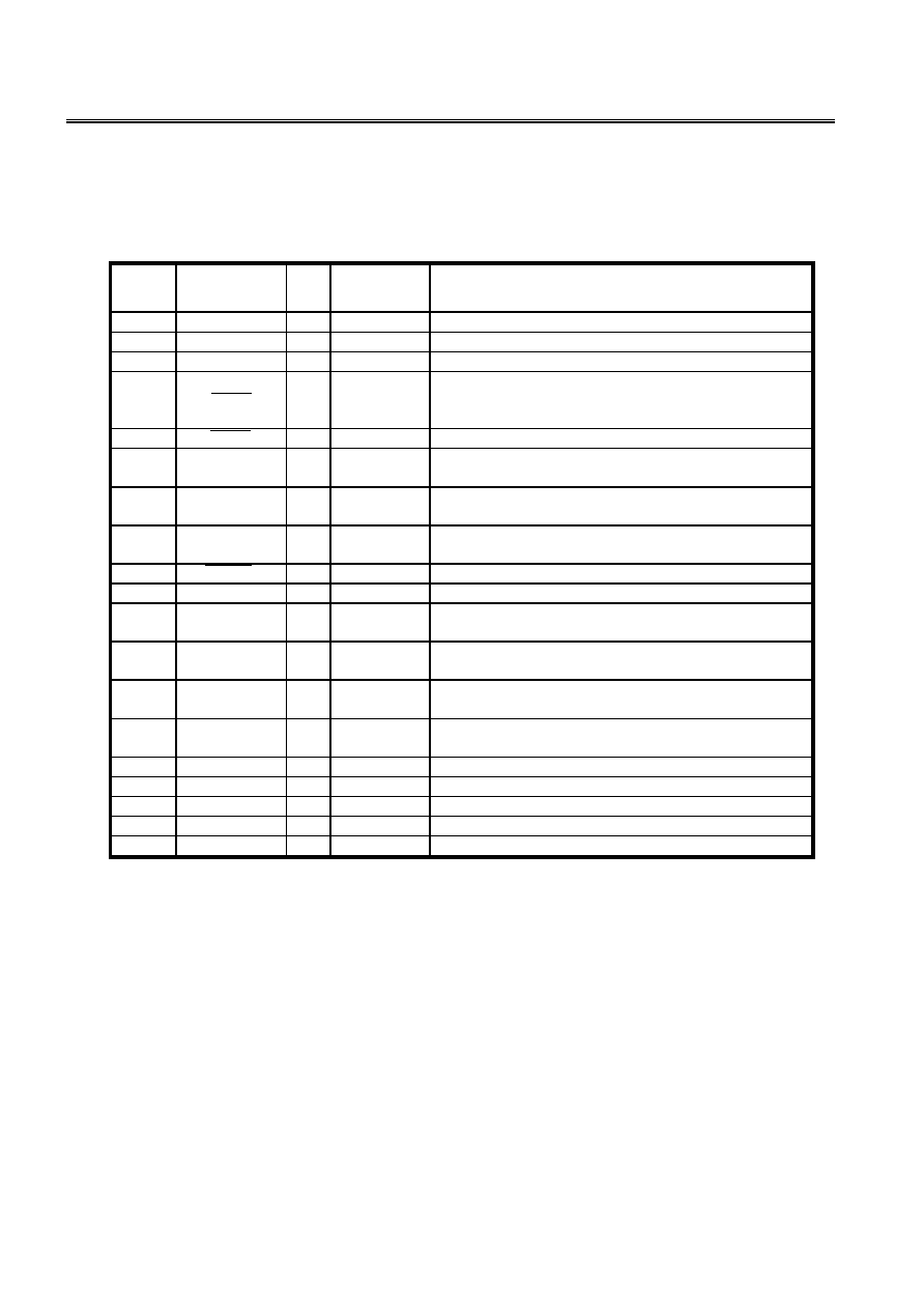
Function of Each Pin
Table 2 Function of Each Pin
Pin No.
Name
I/O
Reset State
Description
1
X
OUT
O
-
Oscillating Circuit Output Pin
2
V
SS
-
-
Power Supply Pin (GND)
3
V
IN
I
-
Oscillating Circuit Input Pin
4
TEST
I
I
Pullup Resistor Bulit-In Test Pin:
Data can be written in the Test Register when this pin is
"
L.
"
Normally operates when
"
H
"
or
"
Open.
"
5
SIGIN
I
I
Received Data Input Pin
6
BS1
O
L
Battery Save Signal Output Pin for RF Control:
Can be used as an output port.
7
BS2
O
L
Battery Save Signal Output Pin for Quick Charge:
Can be used as an output port.
8
BS3
O
L
Battery Save Signal Output Pin for PLL Control:
Can be used as an output port.
9
RESET
I
I
Pullup Resister Bulit-In Reset Input Pin
10
V
DD
-
-
Positive Power Supply Pin
11
V
IB
O
Vibrator Drive Pin:
Can be used as an output port.
12
TONE
O
L
Sound Output Pin:
Can be used as an output port.
13 to 14
LED1 to 2
O
L
2-bit LED Drive Pin:
Can be used as an output port.
15 to 18
PIO0 to 3
I/O
I
4-bit Input/Output Port:
Interrupt is possible at the falling edge.
19 to 22
PIO4 to 7
I/O
I
4-bit Input/Output Port
23 to 54
SEG0 to 31
O
-
Segment Signal Output Pin for LCD Driver
55 to 58
COM0 to 3
O
-
Common Signal Output Pin for LCD Driver
58 to 61
1 to 3
-
-
Tripler capacitor Connecting Pin for LCD Driver
62 to 64
V
LC
1 to 3
-
-
Power Supply Pin for LCD Driver

MICROCOMPITER WITH BUILT-IN PAGING DECODER
S-70L01AQS
4
Seiko Instruments Inc.
n
n
Block Diagram
n
n
Absolute Maximum Ratings
Table 3 Absolute Maximum Ratings
Synchro.
Circuit
Error
Corrector
Decoder
Dual Port
RAM
ID Register
LCD
Driver
RAM
512 byte
ROM
8 kbyte
Beep/
Melody
Generator
Input/Output
Port
Output
Port
S65C02
Clock
Controller RTC
TEST
SIGIN
BS3
BS2
BS1
RESET
SEG0 to SEG31
TONE
VIB
8-bit
Timer
Interrupt
LED2
Buffer
LED1
VDD
VSS
COM0 to COM4
PIO4 to 7
PIO0 to 3
Reset
76.8 kHz
X
IN
X
OUT
Interrupt
In/Out Port
Tripler
VLC1-3
1-3
CPU
Watch
Dog
Timer
Item
Symbol
Conditions
Ratings
Unit
Storage Temp. Range
Tstg
-40 to + 125
∞
C
Operating Temp. Range
Topr
-10 to + 55
∞
C
Power Voltage
V
DD
Ta = 25
∞
C
-0.3 to + 4.0
V
Input Voltage
V
IN
Ta = 25
∞
C
-0.3 to V
DD
+ 0.3
V
Output Voltage
V
OUT
Ta = 25
∞
C
-0.3 to V
DD
+ 0.3
V
Power Dissipation
Pd
Ta = 25
∞
C
300
mW
MICROCOMPITER WITH BUILT-IN PAGING DECODER
S-70L01AQS
Seiko Instruments Inc.
5
n
n
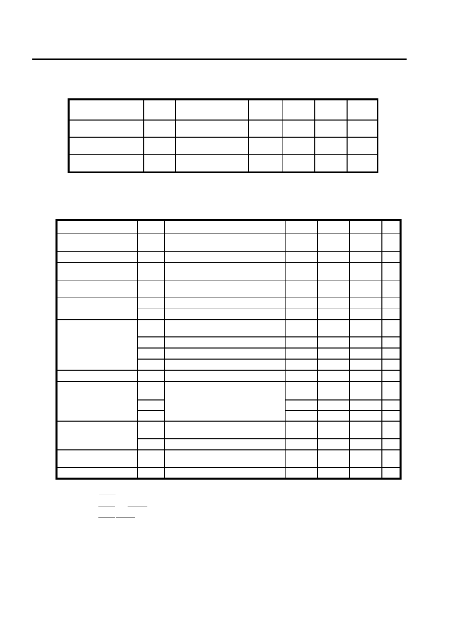
Recommended Operating Conditions
Table 4 Recommended Operating Conditions
Unless otherwise specified: Ta = -10 to + 55
∞
C
n
n
DC Characteristics
Table 5 DC Characteristics
Unless otherwise specified: V
DD
=1.5V, V
SS
=0V, Ta=25
∞
C
*1 Applies to pins BS1, BS2, BS3, VIB, TONE, LED1, LED2, PIO0 through PIO7.
*2 Applies to pins SIGIN,PIO0 through PIO7.
*3 Applies to pins TEST and RESET .
*4 Applies to pins TEST,RESET, PIO0 through PIO7.
*5 Applies to pins SEG0 through SEG31, COM0 through COM3.
Note:
It is recommended to insert a capacitor of 0.1uF or more between pins V
DD
and V
SS
.
Item
Symbol
Conditions
Min.
Typ.
Max.
Unit
Power Voltage
V
DD
at 76.8 kHz
0.9
-
2.2
V
Input Voltage
V
IN
0
-
V
DD
V
Clock Osc. Frequency
fx
V
DD
= 0.9 to 2.2 V
-
76.8
-
kHz
Item
Symbol
Conditions
Min.
Typ.
Max.
Unit
Operating Power Supply
Voltage Range
V
DD
Ta = -10
∞
C to + 55
∞
C at 76.8 kHz
0.9
-
2.2
V
Osc. Start Voltage
V
DOB
Ta = -10
∞
C to + 55
∞
C at 76.8 kHz
0.9
-
2.2
V
Average Current
Consumption during Standby
I
DD1
Ta = -10
∞
C to + 55
∞
C at 76.8 kHz
-
10
30
µ
A
Current Consumption in the
HALT mode
I
DD2
Ta = -10
∞
C to + 55
∞
C at 76.8 kHz
-
6
20
µ
A
Output Current
I
OH1
V
OUT
= 1.2 V *1
-
-500
-150
µ
A
I
OL1
V
OUT
= 0.3 V *1
150
300
-
µ
A
V
IH1
input pin *2
0.8
◊
V
DD
-
-
V
Input Voltage
V
IH1
Schmitt trigger pin *3
0.9
◊
V
DD
-
-
V
V
IL2
input pin *2
-
-
0.2
◊
V
DD
V
V
IL2
Schmitt trigger pin *3
-
-
0.1
◊
V
DD
V
Pullup Current
I
R
V
in
= 0 V *4
-30
-13
-3
µ
A
LCD Voltage
V
LC1
Ta = -10
∞
C to + 50
∞
C, RL = 1M
,
Boosting capacitor = 0.47
µ
F
0.940
1.000
1.060
V
V
LC2
1.816
1.952
2.078
V
V
LC3
2.707
2.910
3.091
LCD High Level Output
Current
I
OH2
V
OUT
= V
LC2
= -0.05 V *5
-
- 10.0
- 3.0
µ
A
I
OH3
V
OUT
= V
LC3
= -0.05 V *5
-
- 10.0
- 3.0
µ
A
LCD Low Level Output
Current
I
OL2
V
OUT
= 0.05 V*5
3.0
12.0
-
µ
A
Schmitt Hysteresis Width
V
WD
Schmitt trigger pin *3
-
0.6
-
V