Rev.1.2
_10
MINI ANALOG SERIES
CMOS SINGLE COMPARATOR
S-892xxA Series
Seiko Instruments Inc.
1
The mini-analog series is a group of ICs that incorporate a general
purpose analog circuit in an ultra-small package.
The S-892xxA Series is a CMOS type single comparator that can be
driven at a lower voltage with lower current consumption than existing
bipolar comparators. These features make this product the ideal
solution for small battery-powered portable equipment.
Features
Application
CMOS
single
comparator
Cellular phones
Low operating voltage:
V
DD
= 1.8 to 5.5 V
Cameras
Low current consumption: I
DD
= 50 µA
(S-89210ACNC)
PDAs
I
DD
= 10 µA
(S-89220ACNC)
Notebook PCs
Low input offset voltage (4.0 mV max.)
Digital cameras
Small package (SC-88A: 2.0 mm
◊
2.1
mm) Digital video cameras
Package
SC-88A (PKG drawing code: NP005-B)
Selection Guide
Table
1
Current consumption
Product Name
I
DD
= 50 µA S-89210ACNC-1C0-TF
I
DD
= 10 µA S-89220ACNC-1C1-TF
Absolute Maximum Ratings
Table 2
Parameter Symbol
Ratings
Unit
Power supply voltage
V
DD
- V
SS
10.0
V
Input voltage
V
IN
V
SS
to V
DD
(7.0 max.)
V
Output voltage
V
OUT
V
SS
to V
DD
(7.0 max.)
V
Differential input voltage
V
IND
±7.0 V
Power dissipation
P
D
200
mW
Operating temperature range
T
opr
-40 to +85
∞C
Storage temperature range
T
stg
-55 to +125
∞C
Caution The absolute maximum ratings are rated values exceeding which the product
could suffer physical damage. These values must therefore not be exceeded
under any conditions.

CMOS SINGLE COMPARATOR
Rev. 1.2
_10
S-892xxA Series
2
Seiko Instruments Inc.
Recommended Operating Power Supply Voltage Range
Table 3
Parameter Symbol
Range
Operating power supply voltage range
V
DD
1.8 to 5.5 V
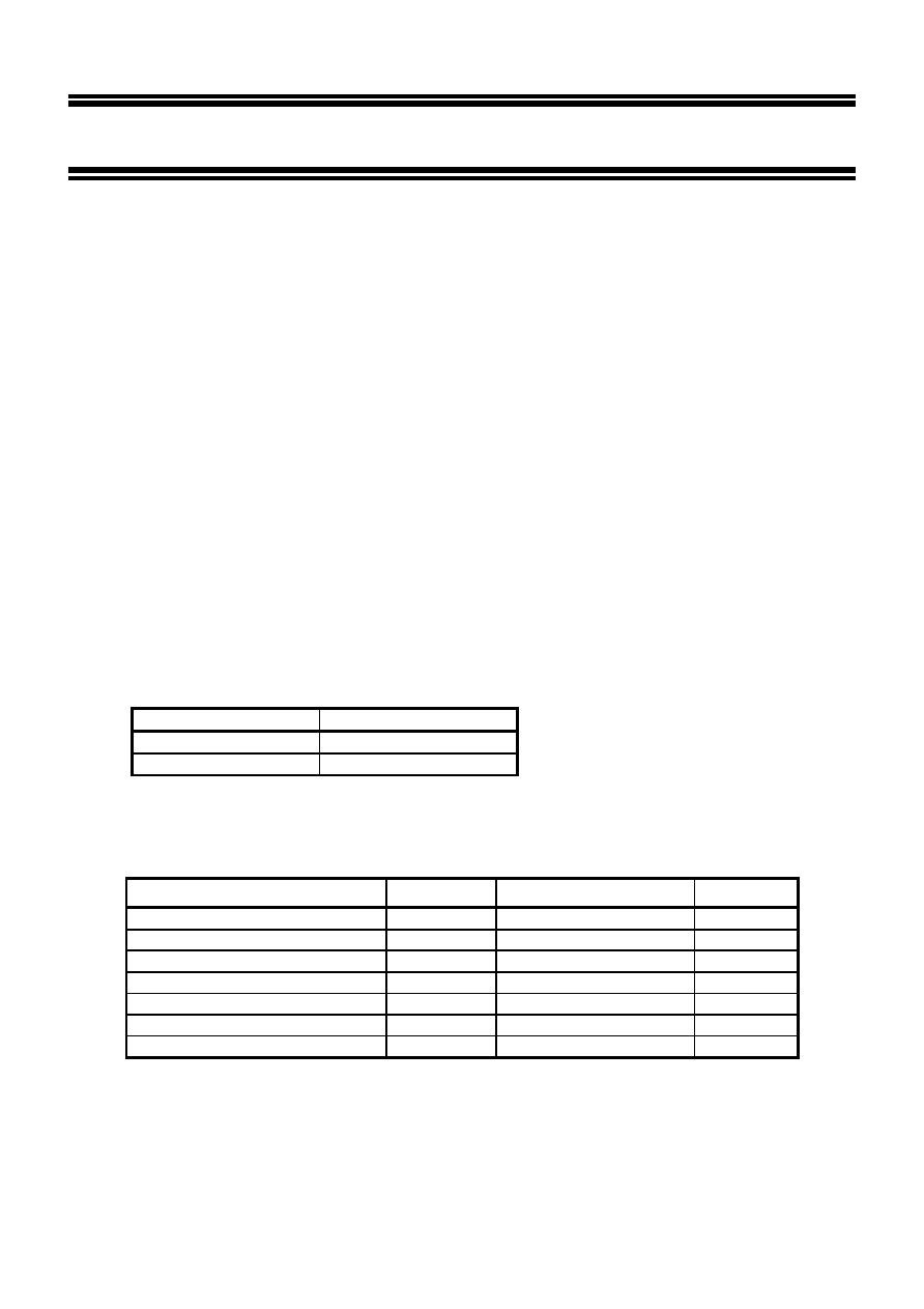
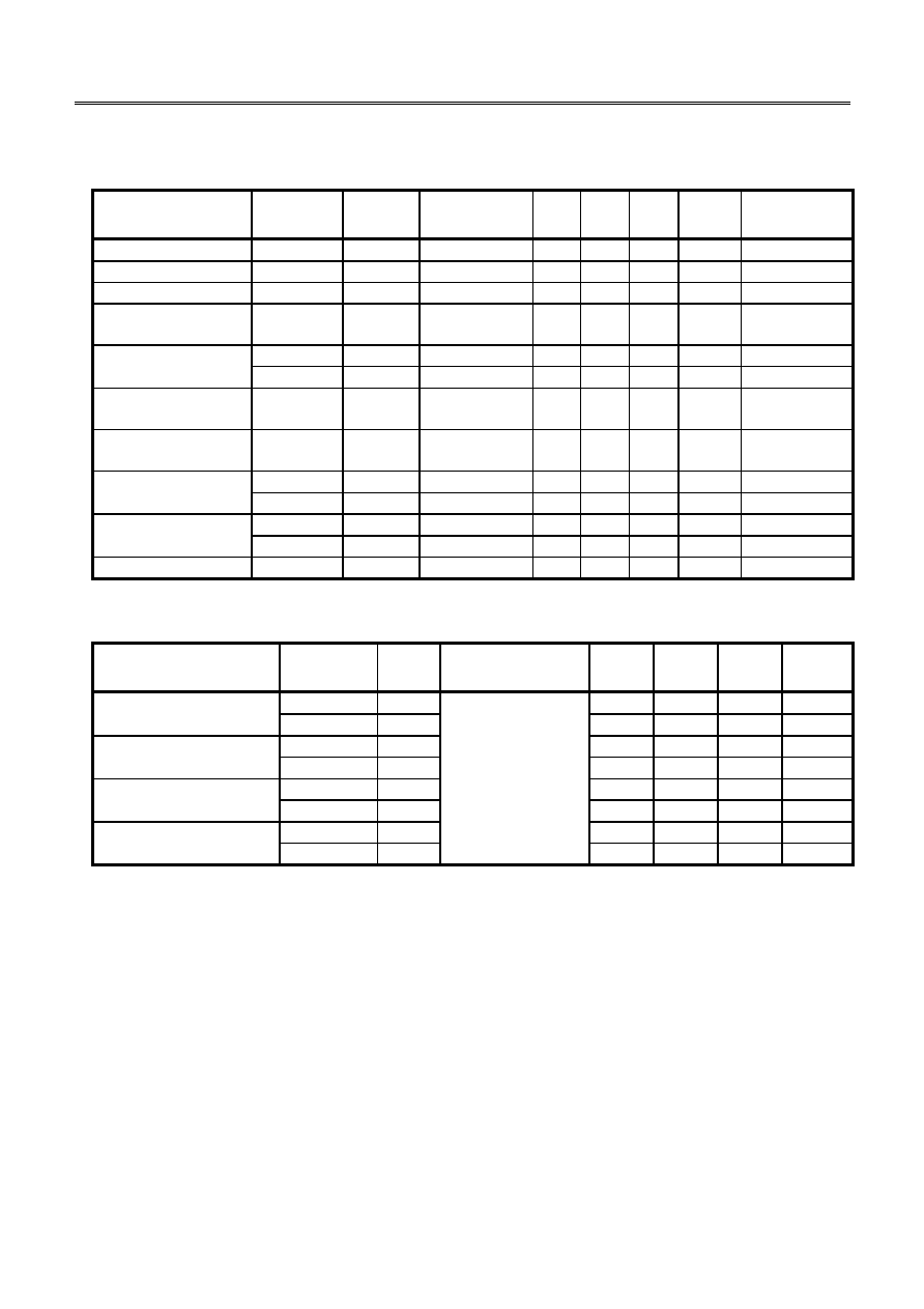
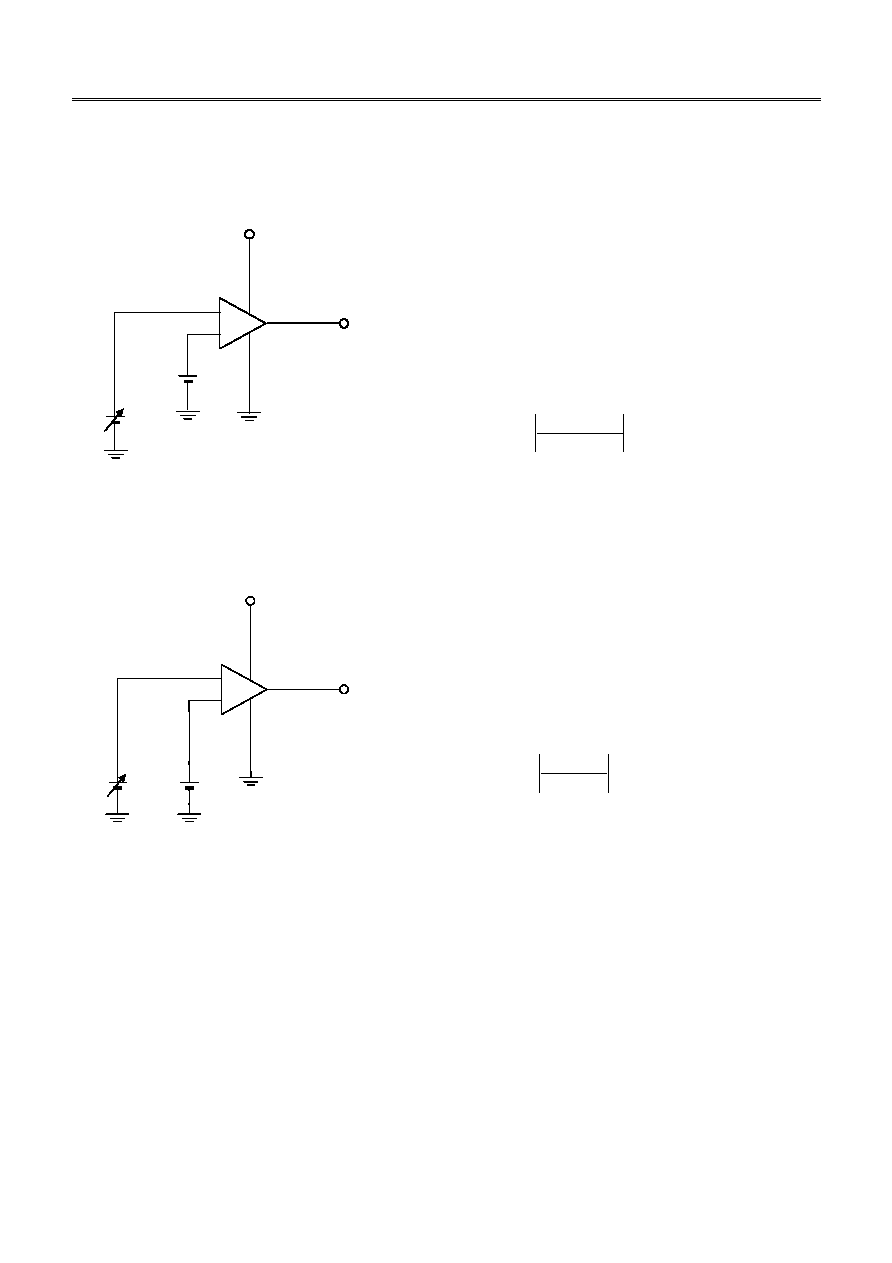
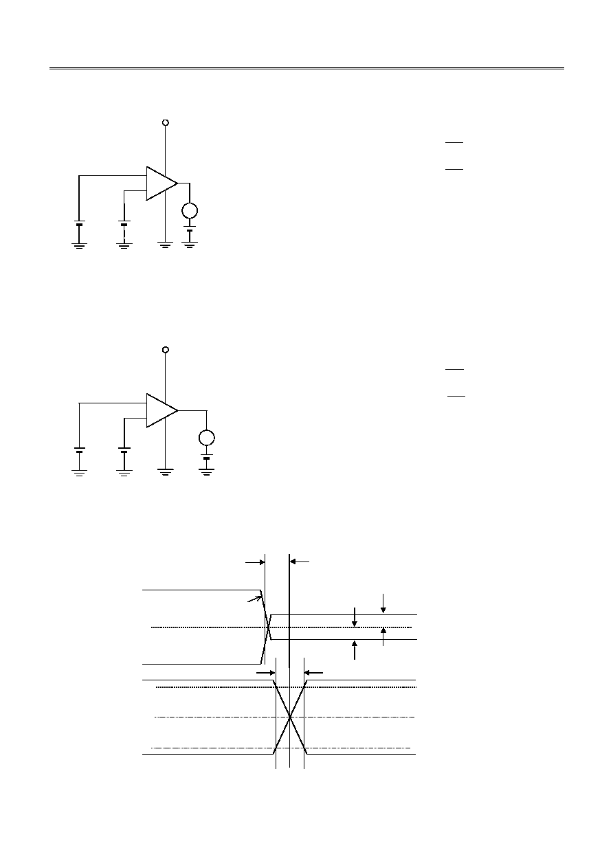
Pin Configuration
Figure
1
[Internal equivalent circuits]
<1> Output pin
<2> Input pin
<3> VDD pin
VDD
VSS
VSS
VDD
VSS
VDD
Figure 2
Figure 3
Figure 4
(S-89210ACNC, S-89220ACNC)
5-Pin SC-88A Top View
VSS
IN(
+)
IN(
-)
VDD
OUT
1
2
3
5
4
Pin No.
Symbol
Description
Internal Equivalent Circuit
1 IN(
+)
Non-inverted input pin
Figure 3
2 VSS
GND
pin
-
3 IN(
-)
Inverted input pin
Figure 3
4
OUT
Output pin
Figure 2
5
VDD
Positive power supply pin
Figure 4
Table 4

Rev.1.2
_10
CMOS SINGLE COMPARATOR
S-892xxA Series
Seiko Instruments Inc.
3
Electrical Characteristics
1. V
DD
= 5.0 V
DC Characteristics (V
DD
= 5.0 V)
Table 5 (Ta
= 25∞C unless otherwise specified)
Parameter Model
No.
Symbol
Measurement
conditions
Min. Typ. Max. Unit Measurement
circuit
Input offset voltage
V
IO
±3
±4 mV Figure
5
Input offset current
I
IO
1 pA
Input bias current
I
BIAS
1 pA
Common-mode input
voltage range
V
CMR
0
4.3 V
Maximum output
V
OH
I
OH
= 20 µA
4.7
V Figure
7
swing voltage
V
OL
I
OL
= 20 µA
0.01 V
Figure
8
Common-mode input
signal rejection ratio
CMRR 60
70
dB Figure
6
Power supply voltage
rejection ratio
PSRR 60
70
dB Figure
5
S-89210A
I
DD
50 120 µA Figure
9
S-89220A
I
DD
10 30 µA Figure
9
S-89210A
I
SOURCE
V
OH
= 0 V
120
µA Figure
10
S-89220A
I
SOURCE
V
OH
= 0 V
25
µA Figure
10
Sink current
I
SINK
V
OL
= 0.5 V
9
mA Figure
11
AC Characteristics (V
DD
= 5.0 V)
Table 6 (Ta
= 25∞C unless otherwise specified)
Parameter Model
No.
Symbol
Measurement
conditions
Min. Typ. Max. Unit
Rise propagation
S-89210A
t
PLH
45
µs
delay time
S-89220A
t
PLH
230
µs
Fall propagation
S-89210A
t
PHL
Overdrive
= 100 mV
9
µs
delay time
S-89220A
t
PHL
C
L
= 15 pF
45
µs
Rise response
S-89210A
t
TLH
(Refer to Figure 12.)
3
µs
time
S-89220A
t
TLH
15
µs
Fall response
S-89210A
t
THL
3
µs
time
S-89220A
t
THL
15
µs
Supply current
Source current
CMOS SINGLE COMPARATOR
Rev. 1.2
_10
S-892xxA Series
4
Seiko Instruments Inc.
2. V
DD
= 3.0 V
DC Characteristics (V
DD
= 3.0 V)
Table 7 (Ta
= 25∞C unless otherwise specified)
Parameter Model
No.
Symbol
Measurement
conditions
Min. Typ. Max. Unit Measurement
circuit
Input offset voltage
V
IO
±3
±4 mV Figure
5
Input offset current
I
IO
1 pA
Input bias current
I
BIAS
1 pA
Common-mode input
voltage range
V
CMR
0
2.3 V
Maximum output
V
OH
I
OH
= 20 µA
2.7
V Figure
7
swing voltage
V
OL
I
OL
= 20 µA
0.01 V
Figure
8
Common-mode input
signal rejection ratio
CMRR 60
70
dB Figure
6
Power supply voltage
rejection ratio
PSRR 60
70
dB Figure
5
S-89210A
I
DD
50 120 µA Figure
9
S-89220A
I
DD
10 30 µA Figure
9
S-89210A
I
SOURCE
V
OH
= 0 V
120
µA Figure
10
S-89220A
I
SOURCE
V
OH
= 0 V
25
µA Figure
10
Sink current
I
SINK
V
OL
= 0.5 V
8
mA Figure
11
AC Characteristics (V
DD
= 3.0 V)
Table 8 (Ta
= 25∞C unless otherwise specified)
Parameter Model
No.
Symbol
Measurement
conditions
Min. Typ. Max. Unit
Rise propagation
S-89210A
t
PLH
30
µs
delay time
S-89220A
t
PLH
150
µs
Fall propagation
S-89210A
t
PHL
Overdrive
= 100 mV
6
µs
delay time
S-89220A
t
PHL
C
L
= 15 pF
30
µs
Rise response
S-89210A
t
TLH
(Refer to Figure 12.)
2
µs
time
S-89220A
t
TLH
10
µs
Fall response
S-89210A
t
THL
2
µs
time
S-89220A
t
THL
10
µs
Supply current
Source current

Rev.1.2
_10
CMOS SINGLE COMPARATOR
S-892xxA Series
Seiko Instruments Inc.
5
3. V
DD
= 1.8 V
DC Characteristics (V
DD
= 1.8 V)
Table 9 (Ta
= 25∞C unless otherwise specified)
Parameter Model
No.
Symbol
Measurement
conditions
Min. Typ. Max. Unit Measurement
circuit
Input offset voltage
V
IO
±3
±4 mV Figure
5
Input offset current
I
IO
1 pA
Input bias current
I
BIAS
1 pA
Common-mode input
voltage range
V
CMR
0
1.1 V
Maximum output
V
OH
I
OH
= 20 µA
1.5
V Figure
7
swing voltage
V
OL
I
OL
= 20 µA
0.01 V
Figure
8
Common-mode input
signal rejection ratio
CMRR 60
70
dB Figure
6
Power supply voltage
rejection ratio
PSRR 60
70
dB Figure
5
S-89210A
I
DD
50 120 µA Figure
9
S-89220A
I
DD
10 30 µA Figure
9
S-89210A
I
SOURCE
V
OH
= 0 V
100
µA Figure
10
S-89220A
I
SOURCE
V
OH
= 0 V
20
µA Figure
10
Sink current
I
SINK
V
OL
= 0.5 V
5
mA Figure
11
AC Characteristics (V
DD
= 1.8 V)
Table 10 (Ta
= 25∞C unless otherwise specified)
Parameter Model
No.
Symbol
Measurement
conditions
Min. Typ. Max. Unit
Rise propagation
S-89210A
t
PLH
20
µs
delay time
S-89220A
t
PLH
100
µs
Fall propagation
S-89210A
t
PHL
Overdrive
= 100 mV
5
µs
delay time
S-89220A
t
PHL
C
L
= 15 pF
25
µs
Rise response
S-89210A
t
TLH
(Refer to Figure 12.)
1.2
µs
time
S-89220A
t
TLH
6
µs
Fall response
S-89210A
t
THL
1.2
µs
time
S-89220A
t
THL
6
µs
Supply current
Source current
CMOS SINGLE COMPARATOR
Rev. 1.2
_10
S-892xxA Series
6
Seiko Instruments Inc.
Measurement Circuits
1. Power supply voltage rejection ratio, input offset voltage
-
+
V
OUT
V
DD
V
IN
V
DD
/2
Figure 5
Input offset voltage (V
IO
),
Power supply voltage rejection ratio (PSRR)
The input offset voltage (V
IO
) is defined as VIN when V
OUT
is changed by changing V
IN
to V
DD
/2 level. The power
supply voltage rejection ratio (PSRR) can be calculated by
following expression, with the value of V
IO
measured at
each V
DD
.
Measurement conditions:
When V
DD
= 1.8 V: V
DD
= V
DD1
, V
IO
= V
IO1
When V
DD
= 5.0 V: V
DD
= V
DD2
, V
IO
= V
IO2
(
)
-
-
=
IO2
IO1
DD2
DD1
V
V
V
V
20log
PSRR
2. Common-mode input signal rejection ratio, common-mode input voltage range
+
-
V
OUT
V
DD
V
IN1
V
IN2
Figure 6
Common-mode input signal rejection ratio (CMRR)
The common-mode input signal rejection ratio (CMRR) can
be calculated by the following expression, with the offset
voltage (V
IO
) set as V
IN1
minus V
IN2
after V
OUT
is changed
by changing V
IN1
.
Measurement conditions:
V
DD
= 3.0 V
When V
IN2
= V
CMR
(max.): V
IN2
= V
INH
, V
IO
= V
IO1
When V
IN2
= V
DD
/2: V
IN2
= V
INL
, V
IO
= V
IO2
-
-
=
IO2
IO1
INL
INH
V
V
V
V
20log
CMRR
Common-mode input voltage range (V
CMR
)
The common-mode input voltage range is the range of V
IN2
in which V
OUT
satisfies the common-mode input signal
rejection ratio specifications.

Rev.1.2
_10
CMOS SINGLE COMPARATOR
S-892xxA Series
Seiko Instruments Inc.
7
3. Maximum output swing voltage (V
OH
)
V
IN2
+
-
V
OH
V
DD
V
IN1
V
I
OH
Figure 7
Maximum output swing voltage (V
OH
)
Measurement conditions:
V
0.5
2
V
V
DD
IN1
-
=
V
0.5
2
V
V
DD
IN2
+
=
I
OH
= 20 µA
4. Maximum output swing voltage (V
OL
)
V
IN2
+
-
V
OL
V
DD
V
IN1
V
I
OL
Figure 8
Maximum output swing voltage (V
OL
)
Measurement conditions:
V
0.5
2
V
V
DD
IN1
+
=
V
0.5
2
V
V
DD
IN2
-
=
I
OL
= 20 µA
5. Supply current (I
DD
)
V
IN1
V
IN2
+
-
V
OUT
V
DD
A
Figure 9
Supply current (I
DD
)
Measurement conditions: V
IN1
= V
SS
V
IN2
= V
DD
CMOS SINGLE COMPARATOR
Rev. 1.2
_10
S-892xxA Series
8
Seiko Instruments Inc.
6. Source current (I
SOURCE
)
V
IN2
+
-
V
DD
A
V
IN1
V
OH
= 0 V
Figure 10
Source current (I
SOURCE
)
Measurement conditions:
V
0.5
2
V
V
DD
IN1
-
=
V
0.5
2
V
V
DD
IN2
+
=
7. Sink current (I
SINK
)
V
IN2
+
-
V
DD
A
V
IN1
V
OL
= 0.5 V
Figure 11
Sink current (I
SINK
)
Measurement conditions:
V
0.5
2
V
V
DD
IN1
+
=
V
0.5
2
V
V
DD
IN2
-
=
8. Propagation delay time/transient response time
V
OUT
V
OUT
V
OH
= V
DD
◊ 0.9
V
OL
= V
DD
◊ 0.1
100 mV
100 mV
IN(
-) = V
DD
/2
IN(
+)
IN(
+)
t
PLH
t
PHL
t
TLH
t
THL
Input rise/fall time: 20 ns
Figure 12

Rev.1.2
_10
CMOS SINGLE COMPARATOR
S-892xxA Series
Seiko Instruments Inc.
9
Precaution
Do not apply an electrostatic discharge to this IC that exceeds the performance ratings of the built-in
electrostatic protection circuit.
CMOS SINGLE COMPARATOR
Rev. 1.2
_10
S-892xxA Series
10
Seiko Instruments Inc.
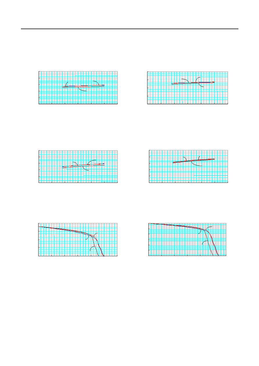
Comparator Characteristics
(All Data Indicates Typical Values for One Circuit)
1. Current consumption vs. Power supply voltage
S-89210 Idd-VDD
@VSS = 0 V
0
20
40
60
80
100
0
1
2
3
4
5
6
VDD [V]
Idd [
µ
A]
100
∞C
25
∞C
-50∞C
S-89220 Idd-VDD
@VSS
= 0 V
0
5
10
15
20
0
1
2
3
4
5
6
VDD [V]
Idd [
µ
A]
100
∞C
25
∞C
-50∞C
2. Output current
2-1. I
SOURCE
vs. Power supply voltage
S-89210 Isource-VDD
@VOH
= 0 V, VSS = 0 V
0
100
200
300
400
500
0
1
2
3
4
5
6
VDD [V]
Is
o
u
r
c
e
[
µ
A]
-50∞C
100
∞C
25
∞C
S-89220 Isource-VDD
@VOH
= 0 V, VSS = 0 V
0
20
40
60
80
100
0
1
2
3
4
5
6
VDD [V]
Is
o
u
r
c
e
[
µ
A]
-50∞C
100
∞C
25
∞C
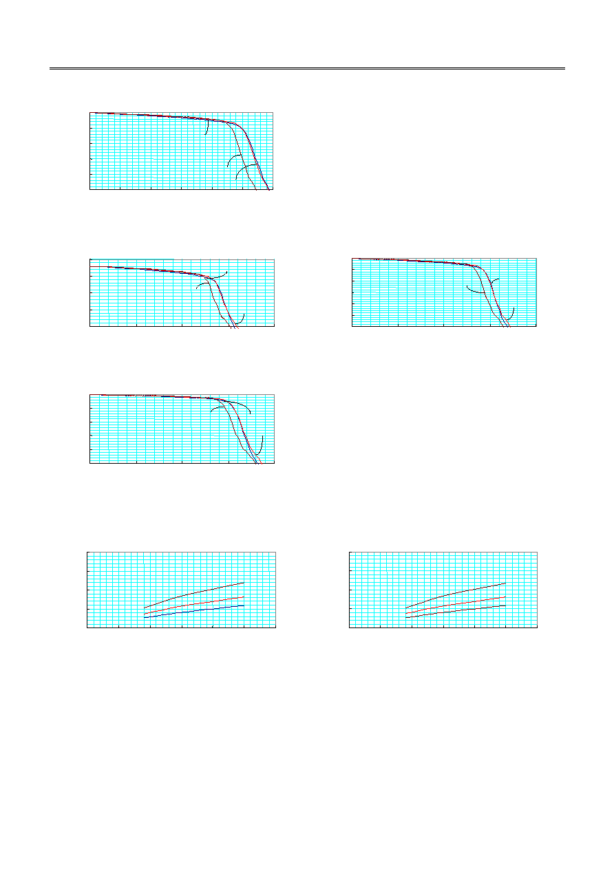
2-2. Output voltage (V
OH
) vs. I
SOURCE
S-89210 Isource-VOH
@VDD
= 1.8 V, VSS = 0 V
0.0
0.5
1.0
1.5
2.0
0
50
100
150
200
Isource [
µA]
VO
H [
V
]
100
∞C
-50∞C
25
∞C
250
300
S-89210 Isource-VOH
@VDD
= 3.0 V, VSS = 0 V
0.0
0.5
1.0
1.5
2.0
2.5
3.0
0
50
100
150
200
Isource [
µA]
VO
H [
V
]
25
∞C
100
∞C
-50∞C
250
300
Rev.1.2
_10
CMOS SINGLE COMPARATOR
S-892xxA Series
Seiko Instruments Inc.
11
S-89210 Isource-VOH
@VDD
= 5.0 V, VSS = 0 V
0.0
1.0
2.0
3.0
4.0
5.0
0
50
100
150
200
Isource [
µA]
VO
H [
V
]
-50∞C
100
∞C
25
∞C
250
300
S-89220 Isource-VOH
@VDD
= 1.8 V, VSS = 0 V
0.0
0.5
1.0
1.5
2.0
0
20
40
Isource [
µA]
VO
H [
V
]
25
∞C
100
∞C
-50∞C
60
80
S-89220 Isource-VOH
@VDD
= 3.0 V, VSS = 0 V
0.0
0.5
1.0
1.5
2.0
2.5
3.0
0
20
40
Isource [
µA]
VO
H [
V
]
100
∞C
-50∞C
25
∞C
60
80
S-89220 Isource-VOH
@VDD
= 5.0 V, VSS = 0 V
0.0
1.0
2.0
3.0
4.0
5.0
0
20
40
60
Isource [
µA]
VO
H [
V
]
-50∞C
100
∞C
25
∞C
80
2-3. I
SINK
vs. Power supply voltage
S-89210 Isink-VDD
@VOL
= 0.5 V, VSS = 0 V
0
10
20
30
40
0
1
2
3
4
5
6
VDD [V]
Is
i
n
k
[
m
A
]
-50∞C
25
∞C
100
∞C
S-89220 Isink-VDD
@VOL
= 0.5 V, VSS = 0 V
0
10
20
30
40
0
1
2
3
4
5
6
VDD [V]
Is
i
n
k
[
m
A
]
-50∞C
25
∞C
100
∞C

CMOS SINGLE COMPARATOR
Rev. 1.2
_10
S-892xxA Series
12
Seiko Instruments Inc.
2-4. I
SINK
vs. Output voltage (V
OL
)
0.0
0.5
1.0
1.5
2.0
0
5
10
15
20
Isink [mA]
VO
L
[
V
]
100
∞C
-50∞C
25
∞C
S-89210 Isink-VOL
@VDD
= 1.8 V, VSS = 0 V
0.0
0.5
1.0
1.5
2.0
2.5
3.0
0
10
20
30
40
Isink [mA]
V
OL [V
]
100
∞C
25
∞C
-50∞C
S-89210 Isink-VOL
@VDD
= 3.0 V, VSS = 0 V
0.0
1.0
2.0
3.0
4.0
5.0
0
20
40
60
80
Isink [mA]
VO
L
[
V
]
-50∞C
25
∞C
100
∞C
S-89210 Isink-VOL
@VDD
= 5.0 V, VSS = 0 V
0.0
0.5
1.0
1.5
2.0
0
5
10
15
20
Isink [mA]
VO
L
[
V
]
100
∞C
25
∞C
-50∞C
S-89220 Isink-VOL
@VDD
= 1.8 V, VSS = 0 V
0.0
0.5
1.0
1.5
2.0
2.5
3.0
0
10
20
30
40
Isink [mA]
VO
L
[
V
]
100
∞C
25
∞C
-50∞C
S-89220 Isink-VOL
@VDD
= 3.0 V, VSS = 0 V
0.0
1.0
2.0
3.0
4.0
5.0
0
20
40
60
80
Isink [mA]
VO
L
[
V
]
100
∞C
25
∞C
-50∞C
S-89220 Isink-VOL
@VDD
= 5.0 V, VSS = 0 V

2.0±0.2
1.3±0.1
0.15
+0.1
-0.05
0.65
0.65
1
2
3
4
5
n SC-88A
lDimensions
Unit mm
lTaping Specifications
lReel Specifications
No.:NP005-B-P-SD-1.0
NP005-B
Rev.1.1
020517
No. : NP005-B-C-SD-1.0
No. : NP005-B-R-SD-2.0
3000 pcs/reel
(2.25)
4.0±0.1 2.0±0.1
4.0±0.1
¯1.55±0.1
¯1.05±0.1
0.2±0.05
1.1±0.1
2.05±0.1
0.3
TF
1
2
3
4
5
Feed direction
12.5max.
9.0±0.3
¯13±0.2
(60∞) (60∞)
Winding core
0.2
+0.1
-0.05

∑
The information described herein is subject to change without notice.
∑
Seiko Instruments Inc. is not responsible for any problems caused by circuits or diagrams described herein
whose related industrial properties, patents, or other rights belong to third parties. The application circuit
examples explain typical applications of the products, and do not guarantee the success of any specific
mass-production design.
∑
When the products described herein are regulated products subject to the Wassenaar Arrangement or other
agreements, they may not be exported without authorization from the appropriate governmental authority.
∑
Use of the information described herein for other purposes and/or reproduction or copying without the
express permission of Seiko Instruments Inc. is strictly prohibited.
∑
The products described herein cannot be used as part of any device or equipment affecting the human
body, such as exercise equipment, medical equipment, security systems, gas equipment, or any apparatus
installed in airplanes and other vehicles, without prior written permission of Seiko Instruments Inc.
∑
Although Seiko Instruments Inc. exerts the greatest possible effort to ensure high quality and reliability, the
failure or malfunction of semiconductor products may occur. The user of these products should therefore
give thorough consideration to safety design, including redundancy, fire-prevention measures, and
malfunction prevention, to prevent any accidents, fires, or community damage that may ensue.