 | –≠–ª–µ–∫—Ç—Ä–æ–Ω–Ω—ã–π –∫–æ–º–ø–æ–Ω–µ–Ω—Ç: DFN10 | –°–∫–∞—á–∞—Ç—å:  PDF PDF  ZIP ZIP |
1
Date: 7/20/05
SP7648 Ultra-low Quiescent Current, High Efficiency Boost Regulator © Copyright 2005 Sipex Corporation
SP7648
FEATURES
True Shutdown
700mA Output Current at 3.3V Input; 4.2V
output
92% Efficiency from 2.7V
IN
to 3.3V
OUT
Wide Input Voltage Range: 2.7V to 4.5V
5V Fixed or Adjustable Output
0.3
Switch
Integrated Synchronous Rectifier:0.3
Anti-Ringing Switch Technology
Programmable Inductor Peak Current
Logic Shutdown Control
Low 0.8V or 0.288V Reference Voltage
Small 10 pin DFN or MSOP Package
Low Reference High Efficiency Boost Regulator
APPLICATIONS
LED Driver
Camera Flash
Handheld Portable Devices
DESCRIPTION
The SP7648 is an ultra-low quiescent current, high efficiency step-up DC-DC converter ideal for
single cell Li-Ion or dual cell alkaline battery applications to drive various LEDs. The SP7648
combines low quiescent current and excellent light-load efficiency of PFM control. The SP7648
features synchronous rectification, a 0.3
charging switch, an anti-ringing inductor switch, under-
voltage lockout and programmable inductor peak current. The device can be shut down by a
1nA active LOW shutdown pin. A very low 0.288V reference voltage is optimized for driving a
constant current load.
Æ
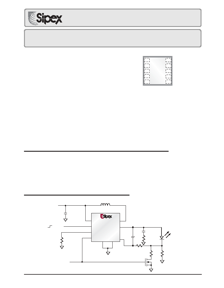
TYPICAL APPLICATION CIRCUIT
Now Available in Lead Free Packaging
SP7648
10 Pin DFN
10
9
8
7
6
1
2
3
4
5
V
OUT
LX
P
GND
GND
FB
FLASH
SHDN
NC (Test)
R
LIM
V
BATT
Preliminary
Æ
4.7
µ
H
V
IN
SP7648
V
BATT
FLASH
FB
LX
V
OUT
NC
1.0K
ON/OFF
10
µ
F
SHDN
GND
10
µ
F
P
GND
0.33
R
LIM
(2.7 - 4.5V)
FLASH
470pF
R
LIM
1K
R
1
R
2
Q
1
D
1

2
Date: 7/20/05
SP7648 Ultra-low Quiescent Current, High Efficiency Boost Regulator © Copyright 2005 Sipex Corporation
LX, Vo, V
BATT
, FLASHOUT, FB to GND pin ...................... -0.3 to 6.0V
SHDN, FLASH ..................................................... -0.3V to V
BATT
+1.0V
Vo, GND, LX Current ....................................................................... 2A
Reverse V
BATT
Current .............................................................. 220mA
Forward V
BATT
Current .............................................................. 500mA
Storage Temperature .................................................. -65
∞
C to 150
∞
C
PARAMETER
MIN
TYP
MAX
UNITS
CONDITIONS
Input Voltage Operating Range, V
BATT
2.7
-
4.5
V
After Startup
Output Voltage Range, V
OUT
2.7
-
5.5
V
Under Voltage Lock-out/UVLO
0.5
0.61
0.7
V
Output Voltage, V
O
4.6
5.0
5.4
V
Internal Feedback Divider
Shutdown Current into V
O,
I
SDO
-
1
500
nA
V
SHDN
= ZeroV
Shutdown Current into V
BATT,
I
SDB
-
250
750
nA
V
SHDN
= ZeroV, V
BATT
= 2.7V
Efficiency
92
-
%
-
V
BATT
= 2.7V, I
OUT
= 200mA, R
LIM
= 2k
Inductor Peak Current Limit, I
PK
650
800
1000
mA
R
LIM
= 2k
, I
PK
= 1600/R
LIM
1600
mA
R
LIM
= 1k
, I
PK
= 1600/R
LIM
Output Current (Note 2)
-
800
-
mA
-
V
BATT
= 2.7V, R
LIM
=1k
-
400
-
mA
-
V
BATT
= 2.7V, R
LIM
=2k
-
200
-
mA
-
V
BATT
= 2.7V, R
LIM
= 4k
Minimum Off-Time Constant K
OFF
0.5
1.0
1.5
V*
µ
s
K
OFF
T
OFF
(V
OUT
- V
BATT
)
Maximum On-Time Constant K
ON
2.0
3.5
5.0
V*
µ
s
K
ON
T
ON
(V
BATT
)
Enable Valid to Output Stable (Note 3)
-
300
500
µ
s
-
I
LOAD
= 1mA
NMOS
Switch Resistance
-
0.30
0.6
I
NMOS
= 100mA
PMOS
Switch Resistance
-
0.30
0.6
I
PMOS
= 100mA
FB Set Voltage, V
FB
0.76
0.8
0.84
V
External feedback Flash = 0
0.266
0.288
0.310
V
External feedback Flash = 1
FB Input Current
-
1
100
nA
V
FB
=1.3V
SHDN Input Voltage (Note 1)
V
IL
-
-
0.5
V
V
BATT
= 2.7V
V
IH
2.0
-
-
V
BATT
= 2.7V
SHDN Input Current
-
1
100
nA
LX Pin Leakage
-
-
3
µ
A
-
FLASH Threshold V
IL
-
-
0.4
V
V
IH
1.0
-
-
V
ELECTRICAL SPECIFICATIONS
V
BATT
=V
SHDN
= 3.6V, V
FB
=ZeroV, I
LOAD
= 0mA, T
AMB
= -40
∞
C to +85
∞
C, V
OUT
= 5.0V, typical values at 27
∞
C unless
otherwise noted. The
denotes the specifications which apply over full operating temperature range -40∫C to +85
∞
C, unless
otherwise specified.
Operating Temperature ................................................ -40
∞
C to +85
∞
C
ESD Rating ........................................................................ 1.5kV HBM
These are stress ratings only and functional operation of the device at
these ratings or any other above those indicated in the operation sections
of the specifications below is not implied. Exposure to absolute maximum
rating conditions for extended periods of time may affect reliability.
ABSOLUTE MAXIMUM RATINGS
Note 1: SHDN must transition faster than 1V/100mS for proper operation.
Note 2: Output Current I =
{
VIN
}
X Efficiency x
{
Inductor Peak Current - Inductor Ripple Current
}
VOUT
2
Note 3: Guaranteed by Design.

3
Date: 7/20/05
SP7648 Ultra-low Quiescent Current, High Efficiency Boost Regulator © Copyright 2005 Sipex Corporation
PIN DESCRIPTION
PIN NUMBER
PIN NAME
DESCRIPTION
1
V
BATT
Battery Voltage. The startup circuitry is powered by this pin. Battery
Voltage is used to calculate switch off time: T
OFF
= K
OFF
/ (V
OUT
-
V
BATT
). When the battery voltage drops below 0.61V the SP7648
goes into an undervoltage lockout mode (UVLO), where the part is shut
down.
2
FLASH
Reference Control Input. Internal Reference defaults to 0.8V if FLASH
= LOW and 0.288V if FLASH = HIGH.
3
NC (Test)
No connection. This pin is bonded out for test purposes only and
must be left floating in all applications.
4
R
LIM
Current Limit Resistor. By connecting a resistor R
LIM
from this pin to
ground the inductor peak current is set by I
PEAK
=1600/R
LIM
. The range
for R
LIM
is 9k
(for 180mA) to 1.K
(for 1.6A).
5
SHDN
Shutdown Not. Tie this pin high to V
BATT,
for normal operation. Pull
this pin to ground to disable all circuitry inside the chip.
6
FB
Feedback. Connect this pin to GND for fixed +5V operation. Connect
this pin to a resistor voltage divider between V
OUT
and GND for
adjustable output operation.
7
GND
Ground. Connect to ground plane.
8
PGND
Power Ground. The inductor charging current flows out of this pin.
9
LX
Inductor Switching Node. Connect one terminal of the inductor to the
positive terminal of the battery. Connect the second terminal of the
inductor to this pin. The inductor charging current flows into LX,
through the internal charging N-channel FET, and out the PGND pin.
10
V
OUT
Output Voltage. The inductor current flows out of this pin during
switch off-time. It is also used as the internal regulator voltage supply.
Connect this pin to the positive terminal of the output capacitor.

4
Date: 7/20/05
SP7648 Ultra-low Quiescent Current, High Efficiency Boost Regulator © Copyright 2005 Sipex Corporation
FUNCTIONAL DIAGRAM

5
Date: 7/20/05
SP7648 Ultra-low Quiescent Current, High Efficiency Boost Regulator © Copyright 2005 Sipex Corporation
_________________________DETAILED
DESCRIPTION
The SP7648 is a step-up DC-DC converter
with an input voltage operation range from
2.7V to 4.7V. In addition to the main 0.3
internal NMOSFET switch the SP7648 has
an internal synchronous rectifier, thereby
increasing efficiency and reducing the space
and cost of an external diode. An internal
inductive-damping switch significantly re-
duces inductive ringing for low noise-high
efficiency operation. If the supply voltage
drops below 0.61V the SP7648 goes into
under voltage lockout, thus opening both
internal switches. The inductor peak current
is externally programmable to allow for a
range of inductor values.
__________________________ CIRCUIT
LAYOUT
Printed circuit board layout is a critical part of
a power supply design. Poor designs can
result in excessive EMI on the feedback
paths and on the ground planes with applica-
tions involving high switching frequencies
and large peak currents. Excessive EMI can
result in instability or regulation errors. All
power components should be placed on the
PC board as closely as possible with the
traces kept short, direct, and wide (>50mils
or 1.25mm). Extra copper on the PC board
should be integrated into ground as a pseudo-
ground plane. On a multilayer PC board,
route the star ground using component-side
copper fill, then connect it to the internal
ground plane using vias. For the SP7648
THEORY OF OPERATION
devices, the inductor and input & output filter
capacitors should be soldered with their
ground pins as close together as possible in
a star-ground configuration. The V
OUT
pin
must be bypassed directly to ground as
close to the SP7648 devices as possible
(within 0.2in or 5mm). The DC-DC converter
and any digital circuitry should be placed on
the opposite corner of the PC board as far
away from sensitive RF and analog input
stages. Noisy traces, such as from the LX
pin, should be kept away from the voltage-
feedback V
FB
node and separated from it
using grounded copper to minimize EMI.
See the SP7648EB Evaluation Board
Manual for PC Board Layout design details.
________________ CONTROL SCHEME
A minimum off-time, current limited pulse
frequency modulation (PFM) control scheme
combines the high output power and effi-
ciency of a pulse width modulation (PWM)
device with the ultra low quiescent current of
the traditional PFM. At low to moderate
output loads the PFM control provides higher
efficiency than traditional PWM converters
are capable of delivering. At these loads the
switching frequency is determined by a mini-
mum off-time (T
OFF
, MIN) and a maximum
on-time (T
ON
, MAX) where:
T
OFF
< K
OFF
/ (V
OUT
- V
BATT
)
T
ON
> K
ON
/ V
BATT
K
OFF
= 1.0V
µ
s
K
ON
= 3.5 V
µ
s