HS3140/SP7514
HS3140/SP7514 14-Bit Multiplying DACs
© Copyright 2000 Sipex Corporation
1
DESCRIPTION...
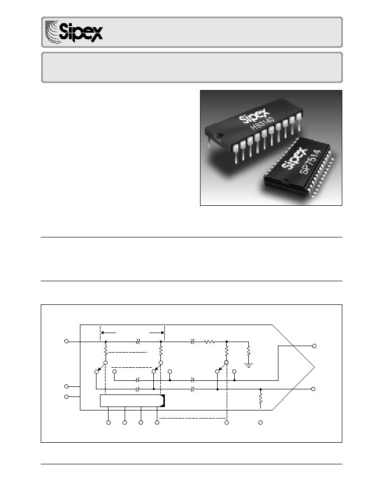
The SP7514 and HS3140 are precision 14-bit multiplying DACs, that provide four-quadrant
multiplication. Both parts accept both AC and DC reference voltages. The SP7514 is available
for use in commercial and industrial temperature ranges, packaged in a 20-pin SOIC. The
HS3140 is available in commercial and military temperature ranges, packaged in a 20-pin
side-brazed DIP.
s
Monolithic Construction
s
14≠Bit Resolution
s
0.003% Non-Linearity
s
Four-Quadrant Multiplication
s
Latch-up Protected
s
Low Power - 30mW
s
Single +15V Power Supply
96k
96k
48k
6k
20
17
SWITCHES ARE
SHOWN IN THE
HIGH STATE
1
I OUT1
R FEEDBACK
BIT 14
LSB
7
6
5
4
BIT 1
(MSB)
BIT 2 BIT 3
BIT 4
4 to 16 DECODE
3
18
GND
VDD
VREF
19
15 EQUAL
SECTIONS
2
I OUT2
96k
96k
SP7514
SP7514, HS3140
Æ
HS3140/SP7514
14-Bit Multiplying DACs
HS3140/SP7514
HS3140/SP7514 14-Bit Multiplying DACs
© Copyright 2000 Sipex Corporation
2
SPECIFICATIONS
(Typical @ 25
∞
C, nominal power supply, V
REF
= +10V, unipolar unless otherwise noted)
PARAMETER
MIN.
TYP.
MAX.
UNITS
CONDITIONS
DIGITAL INPUT
Resolution
14
Bits
2≠Quad, Unipolar Coding
Binary
4≠Quad, Bipolar Coding
Offset Binary
Logic Compatibility
CMOS, TTL
Note 1
Input Current
±
1
µ
A
REFERENCE INPUT
Voltage Range
±
25
V
Note 2
Input Impedance
3.25
9.75
KOhms
ANALOG OUTPUT
Scale Factor
75
225
µ
A/V
REF
Scale Factor Accuracy
±
1
%
Note 3
Output Leakage
10
nA
Note 4
Output Capacitance
C
OUT
1, all inputs high
100
pF
C
OUT
1, all inputs low
50
pF
C
OUT
2, all inputs high
50
pF
C
OUT
2, all inputs low
100
pF
STATIC PERFORMANCE
Integral Linearity
Note 5
SP7514KN/BN, HS3140≠4
±
0.003
±
0.006
% FSR
SP7514JN/AN, HS3140≠3
±
0.006
±
0.012
% FSR
Differential Linearity
Note 6
SP7514KN/BN, HS3140≠4
±
0.003
±
0.006
%FSR
SP7514JN/AN, HS3140≠3
±
0.006
±
0.012
% FSR
Monotonicity
SP7514KN/BN, HS3140≠4
Guaranteed to 14 bits
SP7514JN/AN, HS3140≠3
Guaranteed to 13 bits
STABILITY
(T
MIN
to T
MAX
)
Scale Factor
4
ppm FSR/
∞
C
Note 7 and 8
Integral Linearity
0.5
1.0
ppm FSR/
∞
C
Differential Linearity
0.5
1.0
ppm FSR/
∞
C
Monotonicity Temp. Range
SP7514JN/KN, HS3140C
0
+70
∞
C
SP7514AN/BN
≠40
+85
∞
C
HS3140B
≠55
+125
∞
C
DYNAMIC PERFORMANCE
Digital Small Signal Settling
1.0
µ
S
Digital Full Scale Settling
2.0
µ
S
Reference Feedthrough Error
(V
REF
= 20Vpp)
@ 1kHz
200
µ
V
@ 10kHz
2
mV
Reference Input Bandwidth
1
MHz
POWER SUPPLY (V
DD
)
Operating Voltage
+15
±
5%
V
Voltage Range
+8
+18
V
Current
2.0
mA
Note 9
Rejection Ratio
0.005
%/%
HS3140/SP7514
HS3140/SP7514 14-Bit Multiplying DACs
© Copyright 2000 Sipex Corporation
3
0.048%
0.024%
0.012%
0.006%
0.003%
4
LINEARITY - %
6
8
10
12
14
16
18
V DD -VOLTS
Linearity vs. Supply Voltage
2.5
4
10
I
6
8
10
12
14
16
18
2.0
1.5
1.0
DD
-mA
V
DD
-VOLTS
Power Supply Current vs. Voltage
0.048
0.024
0.012
0.006
0.003
0.01
0.1
1
10
INTEGRAL LINEARITY ERROR - %
VREF -VOLTS
Integral Linearity Error vs. Reference Voltage
50
40
30
20
10
0
0
10
20
30
40
50
2 LSB
1 LSB
1/2 LSB @ 16 BITS
LINEARITY ERROR - PPM
VOS-mV
Additional Linearity Error vs. Output-Amplifier
Offset-Voltage (V
REF
= + 10V)
0.01
4
GAIN CHANGE - %
6
8
10
12
14
16
18
0.004
0.002
0
V
DD
-VOLTS
0.008
0.006
Gain Change vs. Supply Voltage
CHARACTERISTIC CURVES
(Typical @ + 25
∞
C, V
DD
= + 15VDC, V
REF
= + 10VDC, unless otherwise noted)
SPECIFICATIONS (continued)
(Typical @ 25
∞
C, nominal power supply, V
REF
= +10V, unipolar unless otherwise noted)
PARAMETER
MIN.
TYP.
MAX.
UNITS
CONDITIONS
ENVIRONMENTAL AND MECHANICAL
Operating Temperature
SP7514JN/KN
0
+70
∞
C
SP7514AN/BN
≠40
+85
∞
C
HS3140≠C
0
+70
∞
C
HS3140≠B
≠55
+125
∞
C
HS3140≠B/883
≠55
+125
∞
C
Storage Temperature
≠65
+150
∞
C
Package
SP7514_N
20-pin SOIC
HS3140
20≠pin Side≠Brazed DIP
Notes:
1.
Digital input voltage must not exceed supply voltage or go below ≠0.5V ; "0" <0.8V; 2.4V < "1"
V
DD.
2.
AC or DC; use R6758≠1 for fixed reference applications
3.
Using the internal feedback resistor and an external op amp. The Scale Factor can be adjusted externally by variable resistors in series with the
reference input and/or in series to the internal feedback resistor. Please refer to the Applications Information section.
4.
At 25
∞
C; the output leakage current will create an offset voltage at the external op amps output. It doubles every 10
∞
C temperature increase.
5.
Integral Linearity is measured as the arithmetic mean value of the magnitudes of the greatest positive deviation and the greatest negative deviation from
the theoretical value for any given input combination.
6.
Differential Linearity is the deviation of an output step form the theoretical value of 1LSB for any two adjacent digital input codes.
7.
At 25
∞
C, the output leakage current will create an offset voltage output. It doubles every 10
∞
C temperature increase.
8.
Using the internal feedback resistor and an external op amp.
9.
Use series 470ohm resistor to limit start-up current.

HS3140/SP7514
HS3140/SP7514 14-Bit Multiplying DACs
© Copyright 2000 Sipex Corporation
4
PIN ASSIGNMENTS...
Pin 1 ≠ IO
1
≠ Current Output 1.
Pin 2 ≠ IO
2
≠ Current Output 2.
Pin 3 ≠ GND ≠ Ground.
Pin 4 ≠ DB
13
≠ MSB, Data Bit 1.
Pin 5 ≠ DB
12
≠ Data Bit 2.
Pin 6 ≠ DB
11
≠ Data Bit 3.
Pin 7 ≠ DB
10
≠ Data Bit 4.
Pin 8 ≠ DB
9
≠ Data Bit 5.
Pin 9 ≠ DB
8
≠ Data Bit 6.
Pin 10 ≠ DB
7
≠ Data Bit 7.
Pin 11 ≠ DB
6
≠ Data Bit 8.
Pin 12 ≠ DB
5
≠ Data Bit 9.
Pin 13 ≠ DB
4
≠ Data Bit 10.
Pin 14 ≠ DB
3
≠ Data Bit 11.
Pin 15 ≠ DB
2
≠ Data Bit 12.
Pin 16 ≠ DB
1
≠ Data Bit 13.
Pin 17 ≠ DB
0
≠ LSB, Data Bit 14.
Pin 18 ≠ V
DD
≠ Positive Supply Voltage.
Pin 19 ≠ V
REF
≠ Reference Voltage Input.
Pin 20 ≠ R
FB
≠ Feedback Resistor.
PRINCIPLES OF OPERATION
The SP7514/HS3140 achieve high accuracy by using
a decoded or segmented DAC scheme to implement
this function. The following is a brief description of
this approach.
The most common technique for building a D/A
converter of n bits is to use n switches to turn n current
or voltage sources on or off. The n switches and n
sources are designed so that each switch or bit contrib-
utes twice as much to the D/A converter's output as the
preceding bit. This technique is commonly known as
binary weighting and allows an n-bit converter to
generate 2
n
output levels by turning on the proper
combination of bits.
In such binary-weighted converter, the switch
with the smallest contribution (the LSB) accounts
for only 2
-n
of the converter's full-scale value.
Similarly, the switch with the largest contribution
(the MSB) accounts for 2
-1
or half of the converter's
full-scale output. Thus it is easy to see that a given
percent change in the MSB will have a greater
effect on the converter's output than would a
similar percent change in the LSB. For example, a
1% change in the LSB of a 10 bit converter would
only affect the output by 0.001% of full-scale. A
1% change in the MSB of the same converter
would affect the output by 0.5% of FSR.
In order to overcome the problem which results from
the large weighting of the MSB, the two MSB's can
be decoded to three equally weighted sources. Table
1 shows that all combinations of the two MSB's of a
converter result in four output levels. So by replacing
the two MSB's with three bits equally weighted at 1/
4 full-scale and decoding the two MSB digital inputs
into three lines which drive the equally weighted bits,
the same functional performance can be obtained.
Thus by replacing the two MSB switches of a conven-
tional converter with three switches properly de-
coded, the contribution of any switch is reduced from
1/2 to 1/4. This reduction in sensitivity also reduces the
FEATURES...
The SP7514 and HS3140 are precision 14-bit multi-
plying DACs. The DACs are implemented as a one-
chip CMOS circuit with a resistor ladder network.
Three output lines are provided on the DACs to allow
unipolar and bipolar output connection with a mini-
mum of external components. The feedback resistor
is internal. The resistor ladder network termination is
externally available, thus eliminating an external re-
sistor for the 1 LSB offset in bipolar mode.
The SP7514 is available for use in commercial and
industrial temperature ranges, packaged in a 20-pin
SOIC. The HS3140 is available in commercial
and military temperature ranges, packaged in a
20≠pin side≠brazed DIP. For product processed
and screened to the requirements of MIL≠M≠
38510 and MIL≠STD≠883C, please consult the
factory (HS3140B only).
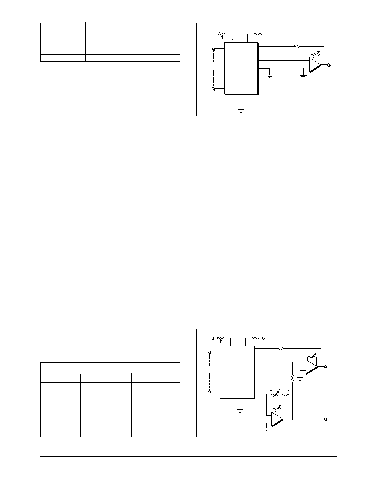
Figure 1. SP7514/HS3140 Equivalent Output Circuit
+
≠
EO
Cf
C
Rp
Rf
CO
Ri
VREF
HS3140/SP7514
HS3140/SP7514 14-Bit Multiplying DACs
© Copyright 2000 Sipex Corporation
5
2
-
1
(MSB)
2
-
2
Output
0
0
0
0
1
1/4 Full-Scale
1
0
1/2 Full-Scale
1
1
3/4 Full-Scale
Table 1. Contribution of the two MSB's
VREF
VDD
470
DIGITAL
INPUTS
RFEEDBACK
I O1
+
-
I O2
GND
ROS
A
V OUT
SP7514
HS3140
200
400
Figure 2. Unipolar Operation
accuracy required of any switch for a given overall
converter accuracy.
With the decoded converter described above, a 1%
change in any of the converter's switches will affect
the output by no more than 0.25% of full-scale as
compared to 0.5% for a conventional converter. In
other words the conventional D/A converter can be
made less sensitive to the quality of its individual bits
by decoding.
In the SP7514/HS3140 the first four MSB's are
decoded into 16 levels which drive 15 equally weighted
current sources. The sensitivity of each switch on the
output is reduced by a factor of 8. Each of the 15
sources contributes 6.25% output change rather than
an MSB change of 50% for the common approach.
Following the decoded section of the DAC a standard
binary weighted R-2R approach is used. This divides
each of the 16 levels (or 6.25% of F.S.) into 4096
discrete levels (the 12 LSB's).
Output Capacitance
The SP7514/HS3140 have very low output capaci-
tance (C
O
). This is specified both with all switches ON
and all switches OFF. Output capacitance varies from
50pF to 100pF over all input codes. This low capaci-
tance is due in part to the decoding technique used.
Smaller switches are used with resulting less capaci-
tance. Three important system characteristics are
affected by C
O
and
C
O
; namely digital feedthrough,
settling time, and bandwidth. The DAC output equiva-
lent circuit can be represented as shown in Figure 1.
Digital feedthrough is the change in analog output due
to the toggling conditions on the converter input data
lines when the analog input V
REF
is at 0V. The
SP7514/HS3140 very low C
O
and therefore will yield
low digital feedthrough. Inputs to the DAC can be
buffered. This input latch with microprocessor control
is shown in Figure 4.
Settling time is directly affected by C
O
. In Figure 1, C
O
combines with R
f
to add a pole to the open loop
response, reducing bandwidth and causing excessive
phase shift - which could result in ringing and/or
oscillation. A feedback capacitor, C
f
must be added to
restore stability. Even with C
f
, there is still a zero-pole
mismatch due to R
i
C
O
which is code dependent. This
code dependent mismatch is minimized when C
O
R
i
=
R
f
C
f
. However C
f
must now be made larger to
compensate for worst case
R
i
C
O
- resulting in re-
duced bandwidth and increased settling time. With the
SP7514/HS3140, small values for C
f
must be used.
DIGITAL
INPUTS
RFEEDBACK
I O1
+
-
IO2
GND
ROS1
A
VOUT
1
+
-
A2
ROS2
V OUT1
A1, A2, OP-07
4K
4K
ROS2
R
200
VREF
VDD
470
400
SP7514
HS3140
Figure 3. Bipolar Operation
TRANSFER FUNCTION (N=14)
BINARY INPUT UNIPOLAR OUTPUT BIPOLAR OUTPUT
111...111
≠V
REF
(1 - 2
≠N
)
≠V
REF
(1 ≠ 2
≠(N ≠ 1)
)
100...001
≠V
REF
(1/2 + 2
≠N
)
≠V
REF
(2
≠(N ≠ 1)
)
100...000
≠V
REF
/2
0
011...111
≠V
REF
(1/2 ≠ 2
≠N
)
V
REF
(2
≠(N ≠ 1)
)
000...001
≠V
REF
(2
(N ≠ 1)
)
V
REF
(1 ≠ 2
≠(N ≠ 1)
)
000...000
0
V
REF
Table 2. Transfer Function