 | –≠–ª–µ–∫—Ç—Ä–æ–Ω–Ω—ã–π –∫–æ–º–ø–æ–Ω–µ–Ω—Ç: SP211HEA | –°–∫–∞—á–∞—Ç—å:  PDF PDF  ZIP ZIP |
1
TGoddard/SP207H/9614R0
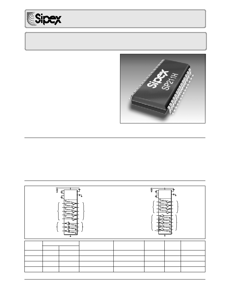
SP207H/SP211H High≠Speed Transceivers
© Copyright 2000 Sipex Corporation
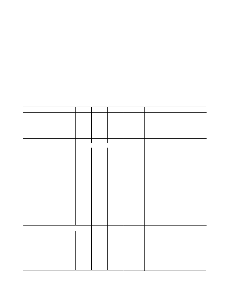
Table 1. Model Selection Table
SP207H/SP211H
+5V High≠Speed RS-232 Transceivers
s
Single 5V Supply Operation
s
0.1
µ
F External Charge Pump Capacitors
s
460kbps Minimum Data Rate
s
Standard SOIC and SSOP Packages
s
SP207H - Five (5) Drivers and Three (3)
Receivers
SP211H - Four (4) Drivers and Five (5)
Receivers
s
1
µ
A Shutdown Mode
s
WakeUp Feature in Shutdown Mode
s
Tri≠State Receiver Outputs
s
Ideal for V.34 and High Speed RS-232
Applications
Number of RS-232
No. of Receivers
No. of External
Model Drivers Receivers
Active in Shutdown 0.1
µ
F Capacitors
Shutdown WakeUp TTL Tri≠State
SP207H
5
3
0
4
No
No
No
SP207HB 5
3
3
4
Yes
Yes
Yes
SP211H
4
5
0
4
Yes
No
Yes
SP211HB 4
5
5
4
Yes
Yes
Yes
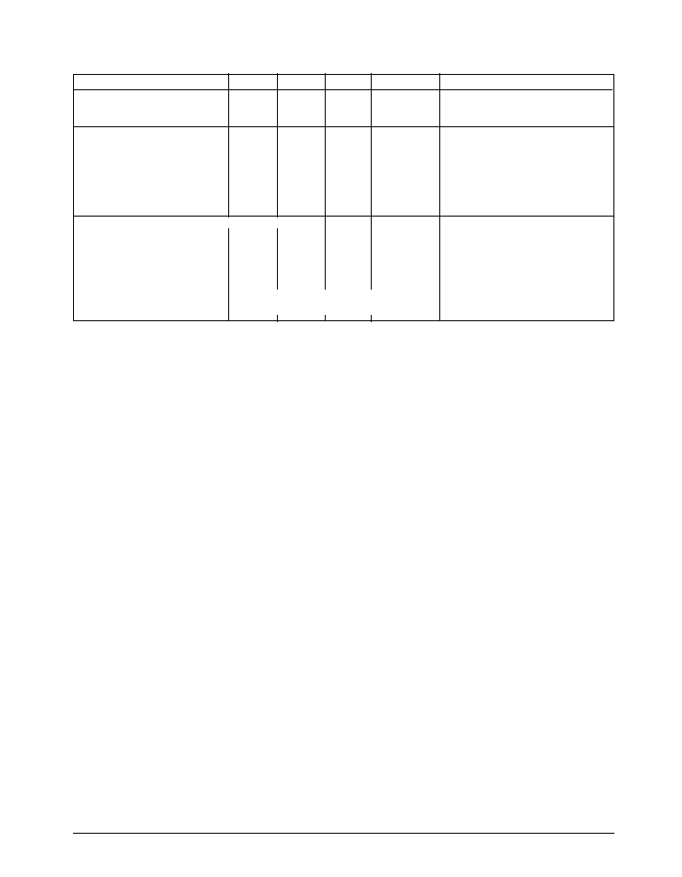
T
1
IN
+5V INPUT
400KOHM
T
1
OUT
0.1µF
6.3V
0.1µF
6.3V
0.1µF
16V
0.1µF
16V
0.1µF
6.3V
+
+
+
+
C
1
+
C
1
≠
C
2
+
C
2
≠
V
+
V
≠
V
CC
T
2
IN
400KOHM
T
2
OUT
T
3
IN
400KOHM
T
3
OUT
T
4
IN
400KOHM
T
4
OUT
R
1
OUT
R
1
IN
10
12
13
14
7
6
18
19
17
9
11
15
2
3
1
24
4
SP207
T
1
T
2
T
3
T
4
8
TTL/CMOS INPUTS
RS-232 OUTPUTS
GND
R
2
OUT
R
2
IN
5
23
R
3
OUT
R
3
IN
22
16
R
1
R
2
R
3
TTL/CMOS OUTPUTS
RS-232 INPUTS
5KOHM
5KOHM
5KOHM
T
5
IN
400KOHM
T
5
OUT
21
20
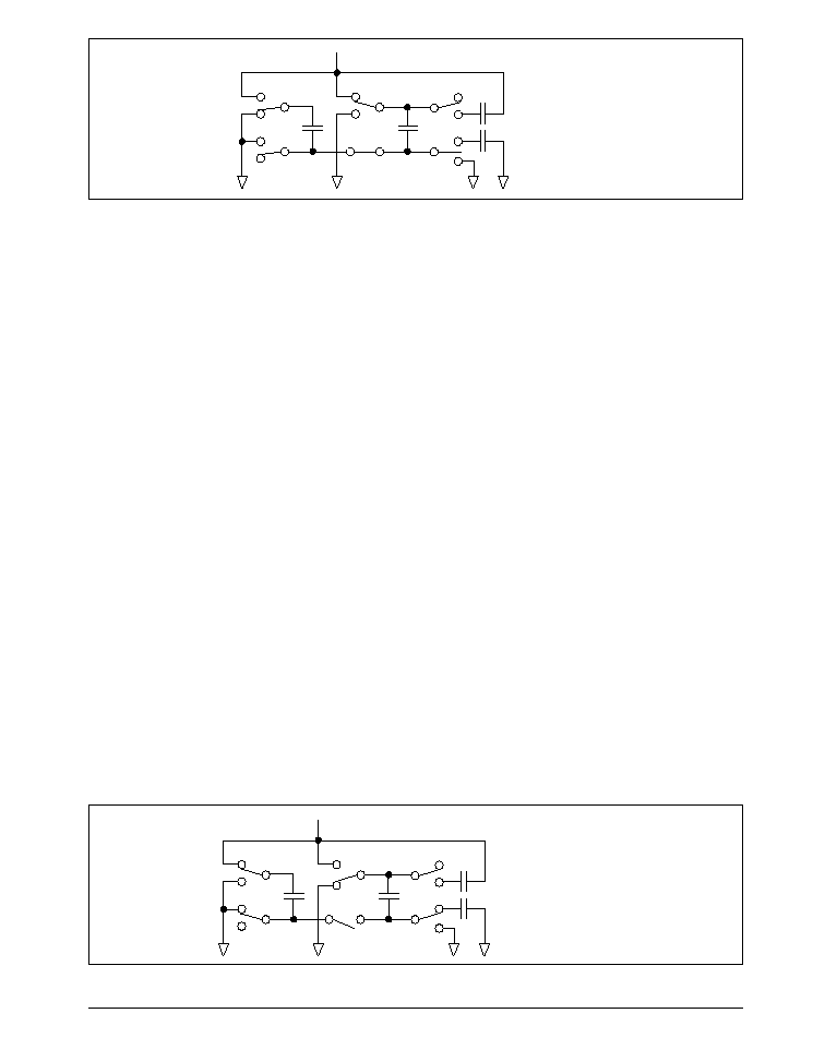
T
5
T1 IN
+5V INPUT
400KOHM
T1 OUT
0.1µF
6.3V
0.1µF
6.3V
0.1µF
16V
0.1µF
16V
0.1µF
6.3V
+
+
+
+
C1 +
C1 ≠
C2 +
C2 ≠
V +
V ≠
VCC
T2 IN
400KOHM
T2 OUT
T3 IN
400KOHM
T3 OUT
T4 IN
400KOHM
T4 OUT
R1 OUT
R1 IN
EN
12
14
15
16
7
6
20
21
8
24
11
13
17
2
3
1
28
9
SP211
T1
T2
T3
T4
10
TTL/CMOS INPUTS
RS-232 OUTPUTS
GND
R2 OUT
R2 IN
5
4
R3 OUT
R3 IN
26
27
R2
R3
TTL/CMOS OUTPUTS
RS-232 INPUTS
5KOHM
5KOHM
5KOHM
R4 OUT
R4IN
22
23
R4
5KOHM
R5 OUT
R5 IN
19
18
R5
5KOHM
SD
25
R1
DESCRIPTION...
The SP207H and SP211H are multi≠channel RS-232 line transceivers configured to fit most
communication needs. The "H" series is based on Sipex's SP200 Series transceivers and has
been enhanced for speed. The data rate is improved to over 460kbps which easily meets the
230.4kbps data rates for V.34. The SP207H and SP211H use the same on-board charge pump
to provide
±
10V voltage levels, using 0.1
µ
F charge pump capacitors to save board space and
reduce circuit cost. The SP207HB, SP211H and SP211HB feature a low≠power shutdown
mode, which reduces power supply drain to 1
µ
A. A WakeUp function keeps the receivers active
in the shutdown mode (SP207HB and SP211HB only).
Æ
TGoddard/SP207H/9614R0
SP207H/SP211H High≠Speed Transceivers
© Copyright 2000 Sipex Corporation
2
ABSOLUTE MAXIMUM RATINGS
These are stress ratings only and functional operation of the device
at these or any other above those indicated in the operation
sections of the specifications below is not implied. Exposure to
absolute maximum rating conditions for extended periods of time
may affect reliability.
V
CC
............................................................................................ +6V
V
+
................................................................. (V
CC
≠ 0.3V) to +13.2V
V
≠
........................................................................................... 13.2V
Input Voltages
Tx
IN
................................................................. ≠0.3V to (V
CC
+0.3V)
Rx
IN
.......................................................................
±
30V at
100mA
Output Voltages
T
OUT
.......................................................... (V
+
, +0.3V) to (V
≠
, ≠0.3V)
R
OUT
................................................................. ≠0.3V to (V
CC
+0.3V)
Short Circuit Duration on T
OUT
....................................... Continuous
Power Dissipation
Plastic DIP .......................................................................... 375mW
(derate 7mW/
∞
C above +70
∞
C)
Small Outline ...................................................................... 375mW
(derate 7mW/
∞
C above +70
∞
C)
SPECIFICATIONS
V
CC
at nominal ratings; 0.1
µ
F charge pump capacitors; T
MIN
to T
MAX
, unless otherwise noted.
PARAMETER
MIN.
TYP.
MAX.
UNIT
CONDITIONS
TTL INPUTS (DRIVER)
T
IN
, EN, SD
Logic Threshold
V
IL
0.8
Volts
V
IH
2.0
Volts
Logic Pullup Current
1.5
10.0
µ
A
T
IN
= 0V
Data Rate
460
600
kbps
C
L
= 1,000pF, R
L
= 3k
TTL OUTPUTS (RECEIVER)
R
OUT
Compatibility
TTL/CMOS
V
OL
0.4
Volts
I
OUT
= 3.2mA; V
CC
= +5V
V
OH
3.5
Volts
I
OUT
= ≠1.0mA
Leakage Current
0.05
±
10
µ
A
EN = V
CC
; 0V
R
OUT
V
CC
;
T
A
= +25
∞
C
RS-232 OUTPUT (DRIVER)
Output Voltage Swing
±
5
±
7
Volts
All transmitter outputs loaded
with 3k
to ground
Power-Off Output Resistance
300
Ohms
V
CC
= 0V; V
OUT
=
±
2V
Output Short Circuit Current
±
25
mA
Infinite duration
RS-232 INPUT (RECEIVER)
Voltage Range
≠15
+15
Volts
Logic Pull Down Current
3.0
10.0
µ
A
T
A
= +25
∞
C
Voltage Threshold
V
IL
0.8
1.2
Volts
V
CC
= +5V, T
A
= +25
∞
C
V
IH
1.7
2.4
Volts
V
CC
= +5V, T
A
= +25
∞
C
Hysteresis
0.2
0.5
1.0
Volts
V
CC
= +5V
Resistance
3
5
7
k
V
IN
=
±
15V; T
A
= +25
∞
C
Data Rate
460
600
kbps
DYNAMIC CHARACTERISTICS
Propagation Delay
1.0
µ
s
TTL≠to≠RS-232
1.5
µ
s
RS-232≠to≠TTL
Instantaneous Slew Rate
60
V/
µ
s
C
L
= 50pF, R
L
= 3≠7k
;
T
A
= +25
∞
C
Transition Region Slew Rate
5
V/
µ
s
C
L
= 1,000pF, R
L
= 3k
;
measured from +3V to
≠3V or ≠3V to +3V
3
TGoddard/SP207H/9614R0
SP207H/SP211H High≠Speed Transceivers
© Copyright 2000 Sipex Corporation
SPECIFICATIONS
V
CC
at nominal ratings; 0.1
µ
F charge pump capacitors; T
MIN
to T
MAX
, unless otherwise noted.
PARAMETER
MIN.
TYP.
MAX.
UNIT
CONDITIONS
Output Enable Time
400
ns
Output Disable Time
250
ns
POWER REQUIREMENTS
V
CC
4.75
5.00
5.25
Volts
I
CC
5
10
mA No load; V
CC
= 5V; T
A
= +25
∞
C
20
mA All transmitters R
L
= 3k
; T
A
= +25
∞
C
Shutdown Current
1
10
µ
A T
A
= +25
∞
C
ENVIRONMENTAL AND MECHANICAL
Operating Temperature
Commercial, ≠C
0
+70
∞
C
Extended, ≠E
≠40
+85
∞
C
Storage Temperature
≠65
+125
∞
C
Package
≠A
Shrink (SSOP) small outline
≠T
Wide (SOIC) small outline

TGoddard/SP207H/9614R0
SP207H/SP211H High≠Speed Transceivers
© Copyright 2000 Sipex Corporation
4
PINOUT
FEATURES...
The SP207H and SP211H line transceivers
provide a variety of configurations to fit most
communication needs, especially those applica-
tions where
±
12V is not available. Both prod-
ucts feature low≠power CMOS construction
and Sipex≠proprietary on-board charge pump
circuitry to generate the
±
10V RS-232 voltage
levels. The ability to use 0.1
µ
F charge pump
capacitors saves board space and reduces circuit
cost.
The SP207HB and SP211H models feature a
low≠power shutdown mode, which reduces
power supply drain to 1
µ
A. The SP207HB and
SP211HB are equipped with the WakeUp func-
tion. The WakeUp function keeps the receivers
active in the shutdown mode, unless disabled by
the EN pin.
SP211
1
2
3
4
5
6
7
8
9
10
11
12
13
14
28
27
26
25
24
23
22
21
20
19
18
17
16
15
T
3
OUT
T
1
OUT
T
2
OUT
R
2
IN
R
2
OUT
T
2
IN
T
1
IN
R
1
OUT
R
1
IN
GND
V
CC
C
1
+
V+
C
1
≠
T
4
OUT
R
3
IN
R
3
OUT
SHUTDOWN (SD)
EN
R
4
IN
R
4
OUT
T
4
IN
T
3
IN
R
5
OUT
R
5
IN
V≠
C
2
≠
C
2
+
SP211B
1
2
3
4
5
6
7
8
9
10
11
12
13
14
28
27
26
25
24
23
22
21
20
19
18
17
16
15
T
3
OUT
T
1
OUT
T
2
OUT
R
2
IN
R
2
OUT
T
2
IN
T
1
IN
R
1
OUT
R
1
IN
GND
V
CC
C
1
+
V+
C
1
≠
T
4
OUT
R
3
IN
R
3
OUT
SHUTDOWN (SD)
EN
R
4
IN
R
4
OUT
T
4
IN
T
3
IN
R
5
OUT
R
5
IN
V≠
C
2
≠
C
2
+
SP207B
1
2
3
4
5
6
7
8
9
10
11
12
13
14
28
27
26
25
24
23
22
21
20
19
18
17
16
15
T
3
OUT
T
1
OUT
T
2
OUT
R
2
IN
R
2
OUT
T
2
IN
T
1
IN
R
1
OUT
R
1
IN
GND
V
CC
C
1
+
V+
C
1
≠
T
4
OUT
NC
T
5
IN
SHUTDOWN (SD)
EN
T
5
OUT
NC
T
4
IN
T
3
IN
R
3
OUT
R
3
IN
V≠
C
2
≠
C
2
+
SP207
1
2
3
4
5
6
7
8
9
10
11
12
24
23
22
21
20
19
18
17
16
15
14
13
T
3
OUT
T
1
OUT
T
2
OUT
R
1
IN
R
1
OUT
T
2
IN
T
1
IN
GND
V
CC
C
1
+
V+
C
1
≠
T
4
OUT
R
2
IN
R
2
OUT
T
5
IN
T
5
OUT
T
4
IN
T
3
IN
R
3
OUT
R
3
IN
V≠
C
2
≠
C
2
+
THEORY OF OPERATION
The SP207H and SP211H are made up of three
basic circuit blocks -- 1) transmitter/driver, 2)
receiver and 3) the Sipex≠proprietary charge
pump.
Charge≠Pump
The charge pump is a Sipex≠patented design
(5,306,954) and uses a unique approach com-
pared to older less≠efficient designs. The charge
pump still requires four external capacitors, but
uses a four≠phase voltage shifting technique to
attain symmetrical 10V power supplies. Figure
3a shows the waveform found on the positive
side of capcitor C
2
, and Figure 3b shows the
5
TGoddard/SP207H/9614R0
SP207H/SP211H High≠Speed Transceivers
© Copyright 2000 Sipex Corporation
Figure 2. Charge Pump -- Phase 2
negative side of capcitor C
2
. There is a free≠
running oscillator that controls the four phases
of the voltage shifting. A description of each
phase follows.
Phase 1
-- V
SS
charge storage --During this phase of the
clock cycle, the positive side of capacitors C
1
and C
2
are initially charged to +5V. C
l
+
is then
switched to ground and the charge in C
1
≠
is
transferred to C
2
≠
. Since C
2
+
is connected to
+5V, the voltage potential across capacitor C
2
is
now 10V.
Phase 2
-- V
SS
transfer -- Phase two of the clock con-
nects the negative terminal of C
2
to the V
SS
storage capacitor and the positive terminal of C
2
to ground, and transfers the generated ≠l0V to
C
3
. Simultaneously, the positive side of capaci-
tor C
1
is switched to +5V and the negative side
is connected to ground.
Phase 3
-- V
DD
charge storage -- The third phase of the
clock is identical to the first phase -- the charge
transferred in C
1
produces ≠5V in the negative
terminal of C
1
, which is applied to the negative
side of capacitor C
2
. Since C
2
+
is at +5V, the
voltage potential across C
2
is l0V.
Phase 4
-- V
DD
transfer -- The fourth phase of the clock
connects the negative terminal of C
2
to ground,
and transfers the generated l0V across C
2
to C
4
,
the V
DD
storage capacitor. Again, simultaneously
with this, the positive side of capacitor C
1
is
switched to +5V and the negative side is con-
nected to ground, and the cycle begins again.
Since both V
+
and V
≠
are separately generated
from V
CC
; in a no≠load condition V
+
and V
≠
will
be symmetrical. Older charge pump approaches
that generate V
≠
from V
+
will show a decrease in
the magnitude of V
≠
compared to V
+
due to the
inherent inefficiencies in the design.
The clock rate for the charge pump typically
operates at 15kHz. The external capacitors can
be as low as 0.1
µ
F with a 16V breakdown
voltage rating.
Transmitter/Driver
The drivers are inverting transmitters which have
been improved for speed over the SP200 Series.
The transmitters accept either TTL or CMOS
inputs and output the RS-232 signals at data rates
over 400kbps. Typically, the RS-232 output volt
V
CC
= +5V
≠5V
≠5V
+5V
V
SS
Storage Capacitor
V
DD
Storage Capacitor
C
1
C
2
C
3
C
4
+
+
+
+
≠
≠
≠
≠
Figure 1. Charge Pump -- Phase 1
V
CC
= +5V
≠10V
V
SS
Storage Capacitor
V
DD
Storage Capacitor
C
1
C
2
C
3
C
4
+
+
+
+
≠
≠
≠
≠