 | –≠–ª–µ–∫—Ç—Ä–æ–Ω–Ω—ã–π –∫–æ–º–ø–æ–Ω–µ–Ω—Ç: SP231ACP | –°–∫–∞—á–∞—Ç—å:  PDF PDF  ZIP ZIP |

SP231ADS/01
SP231A Enhanced RS-232 Line Drivers/Receivers
© Copyright 2000 Sipex Corporation
1
SP231A/232A/233A/310A/312A
s
Operates from Single 5V Power Supply
s
Meets All RS-232D and V.28
Specifications
s
Multiple Drivers and Receivers
s
Small Charge Pump Capacitors ≠
0.1
µ
F
s
Operates with 0.1
µ
F and 100
µ
F
Capacitors
s
High Data Rate ≠ 120kbps Under Load
s
High Output Slew Rate ≠
10V/
µ
s Under Load
s
Low Power Shutdown
1
µ
A
s
3-State TTL/CMOS Receiver Outputs
s
±
30V Receiver Input Levels
s
Low Power CMOS ≠ 15mA Operation
DESCRIPTION...
The Sipex SP231A, SP232A and SP233A are enhanced versions of the Sipex SP231, SP232
and SP233 RS-232 line drivers/receivers. They are pin-for-pin replacements for these earlier
versions and will operate in their sockets. Performance enhancements include 10V/
µ
s slew rate,
120k bits per second guaranteed transmission rate, and increased drive current for longer and
more flexible cable configurations. Ease of use enhancements include smaller, 0.1
µ
F charge
pump capacitors, enhanced ESD protection, low power dissipation and overall ruggedized
construction for commercial environments. The series is available in plastic and ceramic DIP and
SOIC packages operating over the commercial, industrial and military temperature ranges.
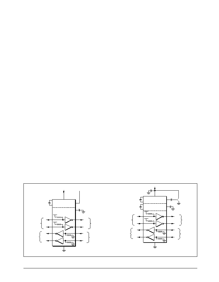
R
2
R
1
T
2
T
1
TTL/CMOS INPUTS
RS-232 OUTPUTS
TTL/CMOS OUTPUTS
RS-232 INPUTS
CHARGE
PUMP
Enhanced RS-232 Line Drivers/Receivers
Æ

SP231ADS/01
SP231A Enhanced RS-232 Line Drivers/Receivers
© Copyright 2000 Sipex Corporation
2
ABSOLUTE MAXIMUM RATINGS
This is a stress rating only and functional operation of the device at
these or any other conditions above those indicated in the operation
sections of this specification is not implied. Exposure to absolute
maximum rating conditions for extended periods of time may affect
reliability.
V
cc
.................................................................................................................................................................
+6V
V
+
....................................................................................................................
(Vcc-0.3V) to +13.2V
V
-
..............................................................................................................................................................
13.2V
Input Voltages
T
IN
.........................................................................................................................
-0.3 to (Vcc +0.3V)
R
IN
............................................................................................................................................................
±
30V
Output Voltages
T
OUT
....................................................................................................
(V+, +0.3V) to (V-, -0.3V)
R
OUT
................................................................................................................
-0.3V to (Vcc +0.3V)
Short Circuit Duration
T
OUT
.........................................................................................................................................
Continuous
Power Dissipation
CERDIP .............................................................................. 675mW
(derate 9.5mW/
∞
C above +70
∞
C)
Plastic DIP .......................................................................... 375mW
(derate 7mW/
∞
C above +70
∞
C)
Small Outline ...................................................................... 375mW
(derate 7mW/
∞
C above +70
∞
C)
SPECIFICATIONS
V
CC
=+5V
±
10%; V+=+8.5V to +13.2V (SP231A only) 0.1
µ
F charge pump capacitors; T
MIN
to T
MAX
unless otherwise noted.
PARAMETERS
MIN.
TYP.
MAX.
UNITS
CONDITIONS
TTL INPUT
Logic Threshold
LOW
0.8
Volts
T
IN
; EN, SD
HIGH
2.0
Volts
T
IN
; EN, SD
Logic Pullup Current
15
200
µ
A
T
IN
= 0V
Maximum Data Rate
120
kbps
C
L
= 2500pF, R
L
= 3k
TTL OUTPUT
TTL/CMOS Output
Voltage, Low
0.4
Volts
I
OUT
= 3.2mA; Vcc = +5V
Voltage, High
3.5
Volts
I
OUT
= -1.0mA
Leakage Current **; T
A
= +25
∞
0.05
±
10
µ
A
EN = V
CC
, 0V
V
OUT
V
CC
RS-232 OUTPUT
Output Voltage Swing
±
5
±
9
Volts
All transmitter outputs loaded
with 3k
to Ground
Output Resistance
300
Ohms
V
CC
= 0V; V
OUT
=
±
2V
Output Short Circuit Current
±
18
mA
Infinite duration
RS-232 INPUT
Voltage Range
-30
+30
Volts
Voltage Threshold
LOW
0.8
1.2
Volts
V
CC
= 5V, T
A
= +25
∞
C
HIGH
1.7
2.4
Volts
V
CC
= 5V, T
A
= +25
∞
C
Hysteresis
0.2
0.5
1.0
Volts
V
CC
= 5V, T
A
= +25
∞
C
Resistance
3
5
7
k
T
A
= +25
∞
C, -15V
V
IN
+15V
DYNAMIC CHARACTERISTICS
Propagation Delay, RS232 to TTL
1.5
µ
s
Instantaneous Slew Rate
30
V/
µ
s
C
L
= 10pF, R
L
= 3-7k
;
T
A
=+25
∞
C
Transition Region Slew Rate
10
V/
µ
s
C
L
= 2500pF, R
L
= 3k
;
measured from +3V to -3V
or -3V to +3V
Output Enable Time **
400
ns
SP310A and SP312A only
Output Disable Time **
250
ns
SP310A and SP312A only
POWER REQUIREMENTS
V
CC
Power Supply Current
10
15
mA
No load, T
A
= +25
∞
C; V
CC
= 5V
25
mA
All transmitters R
L
= 3k
;
T
A
= +25
∞
C
V+ Power Supply Current ***
9
15
mA
No load, V+ = 12V,T
A
=+25
∞
C
Shutdown Supply Current **
1
10
µ
A
V
CC
= 5V, T
A
= +25
∞
C
**SP310A and SP312A only; *** SP231A only

SP231ADS/01
SP231A Enhanced RS-232 Line Drivers/Receivers
© Copyright 2000 Sipex Corporation
3
PERFORMANCE CURVES
-55
-40
0
2
5
7
0
8
5
125
Temperature (∞C)
0
5
10
15
20
25
30
V
CC
= 6V
V
CC
= 5V
V
CC
= 4V
V
CC
= 3V
ICC
(mA)
4.5
4.75
5.0
5.25
5.5
V
CC
(Volts)
6.8
7.4
7.6
7.8
8.0
8.2
8.4
Load current = 0mA
T
A
= 25∞C
VOH
(Volts)
7.0
7.2
0
5
10
15
20
Load Current (mA)
0
6
8
10
12
V+ (Volts)
2
4
V
CC
= 5V
V
CC
= 4V
V
CC
= 6V
25
30
35
40
0246
8
1
0
1
2
1
4
Load Current (mA)
V≠ Voltage (Volts)
-3
-4
-5
-6
-7
-8
-9
-10
-11
V
CC
= 6V
V
CC
= 5V
V
CC
= 4V
PINOUT...
V+
V
CC
GND
T
1
OUT
R
1
IN
R
1
OUT
T
1
IN
C+
C-
V-
T
2
OUT
R
2
IN
R
2
OUT
T
2
IN
SP231A
1
2
3
4
5
6
7
14
13
12
11
10
9
8
14-Pin Plastic DIP
V+
V
CC
GND
T
1
OUT
R
1
IN
R
1
OUT
T
1
IN
NC
C+
C-
V-
T
2
OUT
R
2
IN
R
2
OUT
T
2
IN
NC
16-Pin SOIC
SP231A
1
2
3
4
5
6
7
8
16
15
14
13
12
11
10
9
R OUT
R IN
T OUT
V-
C -
C +
V+
C -
V-
C +
2
1
2
T IN
T IN
R OUT
R IN
T OUT
GND
V
C +
GND
C -
1
2
2
1
2
3
4
5
6
7
8
9
10
20
19
18
17
16
15
14
13
12
11
1
1
1
CC
1
2
2
2
2
SP233ACP
20-PIN PLASTIC DIP
R OUT
R IN
T OUT
V-
C -
C +
C ≠
C +
C +
C ≠
2
1
2
T IN
T IN
R OUT
R IN
T OUT
GND
V
V+
GND
V≠
1
2
2
1
2
3
4
5
6
7
8
9
10
20
19
18
17
16
15
14
13
12
11
1
1
1
CC
2
2
2
2
SP233ACT
1
20-PIN SOIC
V
GND
T OUT
R IN
R OUT
T IN
T IN
R OUT
CC
1
2
C +
V+
C -
C +
C -
V-
T OUT
R IN
1
1
1
SP232A
1
2
3
4
5
6
7
8
16
15
14
13
12
11
10
9
1
2
2
2
2
1
2
SHUTDOWN
V
GND
T OUT
R IN
R OUT
T IN
T IN
R OUT
EN
C +
V+
C -
C +
C -
V-
T OUT
R IN
2
1
2
3
4
5
6
7
8
9
18
17
16
15
14
13
12
11
10
1
1
CC
2
2
SP312A
2
1
2
2
1
1
1
ON/OFF
V
GND
T OUT
R IN
R OUT
T IN
T IN
R OUT
NC
C +
V+
C -
C +
C -
V-
T OUT
R IN
2
1
2
3
4
5
6
7
8
9
18
17
16
15
14
13
12
11
10
1
1
CC
2
2
SP310A
2
1
2
2
1
1
1

SP231ADS/01
SP231A Enhanced RS-232 Line Drivers/Receivers
© Copyright 2000 Sipex Corporation
4
Figure 1. Charge Pump Voltage Doubler
Figure 2. Charge Pump Voltage Inverter
S1
GND
V
CC
+
V+ = 2V
CC
+
V
CC
S2
S3
S4
C1
C3
INTERNAL
OSCILLATOR
S1
FROM
VOLTAGE DOUBLER
V+
+
V- = -(V+)
+
S2
S3
S4
C2
C4
INTERNAL
OSCILLATOR
GND
GND
FEATURES...
The Sipex SP231A, SP232A and SP233A are
enhanced versions of the Sipex SP231, SP232
and SP233 RS-232 line drivers/receivers. They arepin-
for-pin replacements for these earlier versions, will
operate in their sockets with capacitors ranging from
0.1 to 100
µ
F, either polarized or non≠polarized, and
feature several improvements in both performance
and ease of use. Performance enhancements include
10V/
µ
s slew rate, 120k bits per second guaranteed
transmission rate, and increased drive current for
longer and more flexible cable configurations. Ease of
use enhancements include smaller, 0.1
µ
F charge pump
capacitors, enhanced ESD protection, low power
dissipation and overall ruggedized construction for
commercial environments.
The SP232A, SP233A, SP310A and SP312A
include charge pump voltage converters which allow
them to operate from a single +5V supply. These
converters convert the +5V input power to the
±
10V
needed to generate the RS-232 output levels. Both
meet all EIA RS-232D and CCITT V.28 specifica-
tions. The SP231A has provisions for external V+
supplies. With this power supplied externally, the
current drain due to charge pump operation is
considerably reduced, typically to 400
µ
A.
The SP310A provides identical features as the
SP232A. The SP310A has a single control line
which simultaneously shuts down the internal DC/
DC converter and puts all transmitter and receiver
outputs into a high impedance state. The SP312A
is identical to the SP310A with separate tri-state
and shutdown control lines.
The SP231A is available in 14-pin plastic DIP,
CERDIP and 16-pin SOIC packages for opera-
tion over commercial, industrial and military
temperature ranges. The SP232A is available
in 16-pin plastic DIP, SOIC and CERDIP
packages, operating over the commercial,
industrial and military temperature ranges. The
SP233A is available in a 20-pin plastic DIP and
20≠pin SOIC package for operation over the
commercial and industrial temperature ranges.
The SP310A and SP312A are available in
18-pin plastic, CERDIP and SOIC packages
for operation over the commercial and industrial
temperature ranges. Please consult the factory
for DIP and surface-mount packaged parts
supplied on tape-on-reel, as well as parts screened
to MIL-M-38510.
THEORY OF OPERATION
The SP231A, SP232A, SP233A, SP310A and
SP312A devices are made up of three basic circuit
blocks ≠ 1) a driver/transmitter, 2) a receiver and 3)
a charge pump. Each block is described below.
Driver/Transmitter
The drivers are inverting transmitters, which
accept TTL or CMOS inputs and output the
RS-232 signals with an inverted sense relative to
the input logic levels. Typically the RS-232 output
voltage swing is
±
9V. Even under worst case
loading conditions of 3kOhms and 2500pF, the
output is guaranteed to be
±
5V, which is consistent
with the RS-232 standard specifications. The
transmitter outputs are protected against infinite
short-circuits to ground without degradation in
reliability.
The instantaneous slew rate of the transmitter
output is internally limited to a maximum of 30V/
µ
s in order to meet the standards [EIA RS-232-D
2.1.7, Paragraph (5)]. However, the transition
region slew rate of these enhanced products is
typically 10V/
µ
s. The smooth transition of the
loaded output from V
OL
to V
OH
clearly meets the
monotonicity requirements of the standard [EIA
RS-232-D 2.1.7, Paragraphs (1) & (2)].
SP231ADS/01
SP231A Enhanced RS-232 Line Drivers/Receivers
© Copyright 2000 Sipex Corporation
5
R
2
9
8
R IN
R OUT
2
R
1
12
13
R IN
R OUT
1
T
2
10
7
T IN
2
T OUT
2
T
1
11
14
T IN
1
T OUT
1
15
GND
400k
400k
TTL/CMOS INPUTS
RS-232 OUTPUTS
3
1
C +
C -
1
1
6
16
V
CC
V+
+
+
0.1 F
6.3V
µ
+5V to +10V
Voltage Doubler
+5V INPUT
2
V-
TTL/CMOS OUTPUTS
RS-232 INPUTS
2
1
5k
0.1 F
16V
µ
5k
5
4
C +
C -
2
2
+
0.1 F
16V
µ
+10V to -10V
Voltage Inverter
0.1 F 6.3V
µ
10 F 6.3V
µ
SP232A
+
+
*
*The negative terminal of the V+ storage capacitor can be tied
to either V
CC
or GND. Connecting the capacitor to V
CC
(+5V)
is recommended.
Figure 3. Typical Circuits using the SP231A and 232A.
R
2
6
5
R IN
R OUT
2
R
1
9
10
R IN
R OUT
1
T
2
7
4
T IN
2
T OUT
2
T
1
8
11
T IN
1
T OUT
1
12
GND
400k
400k
TTL/CMOS INPUTS
RS-232 OUTPUTS
2
1
C +
C -
1
1
3
13
V
CC
V+
+
+
0.1 F
6.3V
µ
+5V INPUT
14
V-
TTL/CMOS OUTPUTS
RS-232 INPUTS
2
1
5k
0.1 F
16V
µ
5k
+12V to -12V
Voltage Inverter
SP231A
V+ (+8.5V to +13.2V)
Receivers
The receivers convert RS-232 input signals to
inverted TTL signals. Since the input is usually
from a transmission line, where long cable lengths
and system interference can degrade the signal, the
inputs have a typical hysteresis margin of 500mV.
This ensures that the receiver is virtually immune
to noisy transmission lines.
The input thresholds are 0.8V minimum and
2.4V maximum, again well within the
±
3V
RS-232 requirements. The receiver inputs are also
protected against voltages up to
±
30V. Should an
input be left unconnected, a 5kOhm pulldown
resistor to ground will commit the output of the
receiver to a high state.
In actual system applications, it is quite possible
for signals to be applied to the receiver inputs
before power is applied to the receiver circuitry.
This occurs, for example, when a PC user attempts
to print, only to realize the printer wasn't turned on.
In this case an RS-232 signal from the PC will
appear on the receiver input at the printer. When
the printer power is turned on, the receiver will
operate normally. All of these enhanced devices
are fully protected.
Charge Pump
The charge pump section of the these devices
allows the circuit to operate from a single +5V
±
10% power supply by generating the required
operating voltages internal to the devices. The
charge pump consists of two sections -- 1) a
voltage doubler and 2) a voltage inverter.
As shown in Figure 1, an internal oscillator trig-
gers the charge accumulation and voltage inver-
sion. The voltage doubler momentarily stores a
charge on capacitor C
1
equal to V
cc
, referenced to
ground. During the next transition of the oscillator
this charge is boot-strapped to transfer charge to
capacitor C
3
. The voltage across C
3
is now from
V
cc
to V
+
.
In the inverter section (Figure 2), the voltage
across C
3
is transferred to C
2
forcing a range of 0V
to V
+
across C
2
. Boot-strapping of C
2
will then
transfer charge to C
4
to genrate V
-
.
One of the significant enhancements over
previous products of this type is that the values of
the capacitors are no longer critical and have been
decreased in size considerably to 0.1
µ
F. Because
the charge pump runs at a much higher frequency,
the 0.1
µ
F capacitors are sufficient to transfer and
sustain charges to the two transmitters.
APPLICATION HINTS
Protection From Shorts to
±
15V
The driver outputs are protected against shorts
to ground, other driver outputs, and V
+
or V
-
.
If the possibility exists that the outputs could be
inadvertently connected to voltages higher than
±
15V, then it is recommended that external
protection be provided. For protection against
voltages exceeding
±
15V, two back-to-back zener
diodes connected from each output to ground will
clamp the outputs to an acceptable voltage level.