 | Рлектронный компонент: SP301 | Скачать:  PDF PDF  ZIP ZIP |
51
Corporation
SIGNAL PROCESSING EXCELLENCE
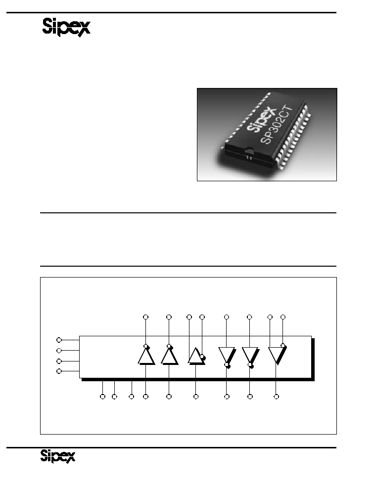
SP301/302
RS-232/RS-422 Line Drivers/Receivers
s
RS-232 and RS-422 on One Chip
s
Multiple Drivers and Receivers
s
Software-selectable Modes
s
Loopback for Self-Testing
s
Short-circuit Protected
s
24-pin Single-width DIP or SOIC
Package
DESCRIPTION...
The SP301 and SP302 are proprietary single-chip devices that contain both RS-232 and RS-422
protocol line drivers and receivers. Their configuration may be changed at any time by logic levels
on two control lines. In any configuration, both the SP301 and SP302 fully meet the requirements
of the EIA RS-232D and RS-422 data communication standards. A loopback test mode is
provided.The SP301 and SP302 are available in 24-pin single width plastic, and 28-pin SOIC
packages for commercial and industrial temperature range operation.
RIB
1
ROB
1
TOB
1
TIB
1
RIA
1
ROA
1
TOA
1
TIA
1
SELECT
A B
TOA
2
RIA
2
TOB
2
TIB
2
RIB
2
ROB
2
V
DD
GND
V
CC
V
EE
SP302
LOOP
BACK
Corporation
SIGNAL PROCESSING EXCELLENCE

Corporation
SIGNAL PROCESSING EXCELLENCE
52
SPECIFICATIONS
(T
MIN
T
A
T
MAX
and nominal supply voltages unless otherwise noted)
PARAMETER
MIN.
TYP.
MAX.
UNITS
CONDITIONS
RS-232 DRIVER
TTL Input Level
V
IL
0
0.8
V
V
IH
2.0
V
High Level Output
+5.0
V
R
L
= 3k
, V
IN
= 0.8V
Low Level Output
-5.0
V
R
L
= 3k
, V
IN
= 2.0V
Short Circuit Current
±
30
mA
V
OUT
= 0V
Loopback Output Voltage
-1.5
V
R
L
= 3k
, V
EE
= -12.0V; Note 1
Slew rate
30
V/
µ
s
C
L
= 50pF, R
L
= 3k
; T
A
= 25
°
C
Transition Time
3
µ
s
V
OUT
from +3V to -3V or
-3V to +3V
Maximum Transmission Rate
200
kbps
RS-232 RECEIVER
Input Voltage Range
-15
+15
V
Note 6
Input High Threshold
+1.75
+2.5
V
Positive-going
Input Low Threshold
+0.75
+1.35
V
Negative-going
Input Impedance
3
7
k
V
SS
V
IN
V
DD
TTL Output Level
V
OL
0.4
V
V
CC
= +4.75V, I
OUT
= +1.6mA
V
OH
2.4
V
V
CC
= +4.75V, I
OUT
= -0.5mA
Maximum Receiving Rate
200
kbps
RS-422 DRIVER
TTL Input Level
V
IL
0
0.8
V
V
IH
2.0
V
High Level Output
2.75
6.0
V
I
OH
= -20mA
Low Level Output
1.0
V
I
OL
= +20mA
Differential Output
±
2
V
R
L
= 100
±
6
V
R
L
=
Short Circuit Current
±
100
mA
Note 2
Output Current
±
500
µ
A
-0.25V
V
O
6V; power off
Transition Time
400
ns
R
L
= 100
, C
L
= 15pF; Note 3
Maximum Transmission Rate
1,000
kbps
RS-422 RECEIVER
Common Mode Range
±
7
V
Note 4
Differential Input
±
15
V
Note 4 and 6
Differential Input Threshold
-0.2
+0.2
V
T
A
= 25
°
C
Input Voltage Hysteresis
30
mV
V
CM
= 0V; T
A
= 25
°
C
Input Resistance
3
k
-7V
V
CM
+7V
TTL Output Level
V
OL
0.4
V
V
CC
= +4.75V, I
OUT
= +1.6mA
V
OH
2.4
V
V
CC
= +4.75V, I
OUT
= -0.5mA
Maximum Receiving Rate
1,000
kbps
Short Circuit Output Current
±
120
mA
V
OUT
= 0V
POWER REQUIREMENTS
V
DD
= +12V,
±
10%
7
15
mA
Note 5
V
CC
= +5V;
±
10%
5
7
mA
Note 5
V
EE
= -12V,
±
10%
11
20
mA
Note 5
ENVIRONMENTAL
Operating Temperature
-CS, CT
0
+70
°
C
-MR
-55
+125
°
C
Storage Temperature
-65
+150
°
C

53
Corporation
SIGNAL PROCESSING EXCELLENCE
Notes:
1.
In Loop-back mode
2.
Only one output drive pin per package will be shorted at any time
3.
From 10% to 90% of steady-state
4.
This is an absolute maximum rating; normal operating levels are V
IN
< 5V
5.
Outputs unloaded; Inputs tied to GND; T
A
= +25
°
C; V
IL
= 0V; LB=0
Typical SP302 current drains under full load are:
18mA (+12V), 10mA (-12V) and 7mA (+5V) in RS-232 mode only;
5mA (+12V), 7mA (-12V) and 56mA (+5V) in RS-422 mode only;
12mA (+12V), 14mA (-12V) and 31mA (+5V) in RS-232 and RS-422 modes;
RS-232 loads 3k
, 2500pF, 20kHz; RS-422 outputs across 100
, 500kHz.
6.
In Loopback mode, the external voltage input to the receiver must not exceed
±
10V, otherwise
the loopback test may be adversely affected.
RS-422 Driver
2V
GND
5V
GND
5V
T
IN
T
OUT
500kHz
5V
GND
10V
GND
10V
T
I N
T
O U T
20kHz
RS-232 Driver
RS-422 Receiver
500kHz
2V
GND
2V
5V
GND
R
IN
R
OUT
20kHz
5V
GND
5V
5V
GND
R
IN
R
OUT
RS-232 Receiver
TYPICAL PERFORMANCE CURVES
Corporation
SIGNAL PROCESSING EXCELLENCE
54
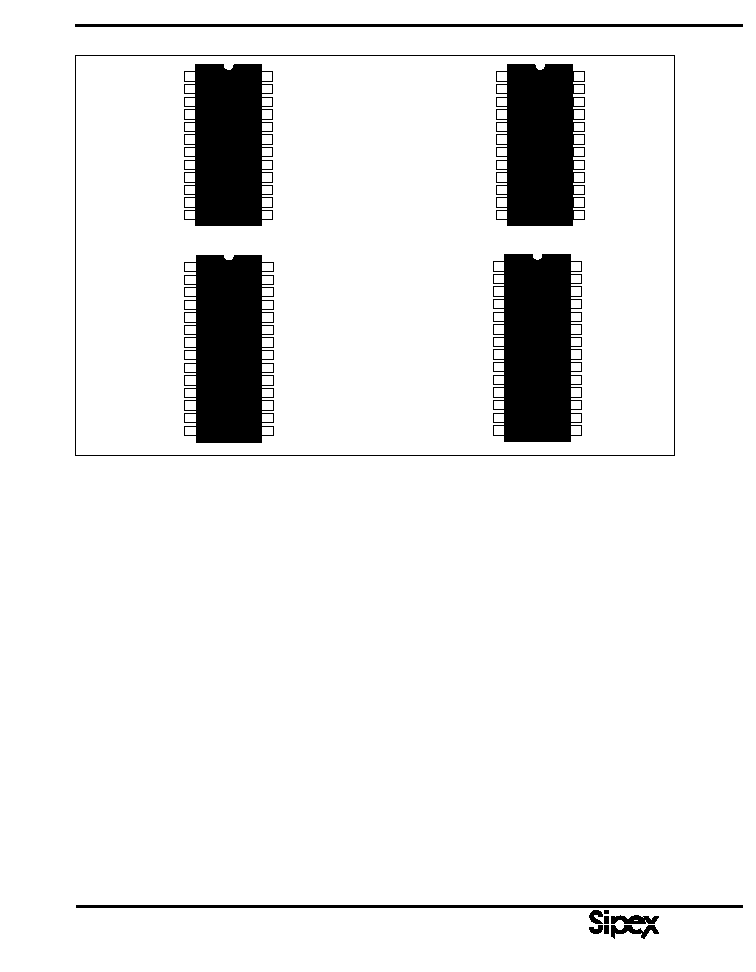
PIN ASSIGNMENTS
SP302CS/MR
V
DD
(+12V) 1
RIA
2
2
RIA
1
3
TOA
2
4
TOA
1
5
SELECT A 6
SELECT B 7
TOB
1
8
TOB
2
9
RIB
1
10
RIB
2
11
GND 12
24 V
CC
(+5V)
23 ROA
2
22 ROA
1
21 TIA
2
20 TIA
1
19 LB
18 N.C.
17 TIB
1
16 TIB
2
15 ROB
1
14 ROB
2
13 V
EE
(-12V)
SP301CS/MR
V
DD
(+12V) 1
RIA
2
2
RIA
1
3
TOA
2
4
TOA
1
5
SELECT A 6
SELECT B 7
TOB
1
8
TOB
2
9
RIB
1
10
RIB
2
11
GND 12
24 V
CC
(+5V)
23 N.C.
22 ROA
21 N.C.
20 TIA
19 LB
18 N.C.
17 TIB
16 N.C.
15 ROB
14 N.C.
13 V
EE
(-12V)
SP302CT
V
DD
(+12V) 1
RIA
2
2
RIA
1
3
N.C. 4
TOA
2
5
TOA
1
6
SELECT A 7
SELECT B 8
TOB
1
9
TOB
2
10
N.C. 11
RIB
1
12
RIB
2
13
GND 14
28 V
CC
(+5V)
27 ROA
2
26 ROA
1
25 N.C.
24 TIA
2
23 TIA
1
22 LB
21 N.C.
20 TIB
1
19 TIB
2
18 N.C.
17 ROB
1
16 ROB
2
15 V
EE
(-12V)
SP301CT
V
DD
(+12V) 1
RIA
2
2
RIA
1
3
N.C. 4
TOA
2
5
TOA
1
6
SELECT A 7
SELECT B 8
TOB
1
9
TOB
2
10
N.C. 11
RIB
1
12
RIB
2
13
GND 14
28 V
CC
(+5V)
27 N.C.
26 ROA
25 N.C.
24 N.C.
23 TIA
22 LB
21 N.C.
20 TIB
19 N.C.
18 N.C.
17 ROB
16 N.C.
15 V
EE
(-12V)
FEATURES...
The SP301 and SP302 are proprietary single-
chip devices that contain both RS-232 and RS-
422 protocol line drivers and receivers. They
differ only in the total number of line drivers and
receivers of each protocol that may be active at
any given time. Their configuration may be
changed at any time by logic levels on two
control lines. In any configuration, both the
SP301 and SP302 fully meet the requirements
of the EIA RS-232D and RS-422 data commu-
nication standards.
The RS-232 line driver circuits convert TTL
logic level inputs into inverted RS-232 output
signals. The RS-422 line drivers convert TTL
logic levels into RS-422 differential output sig-
nals. The RS-422 line driver outputs feature
high source and sink current capability. All line
drivers are internally protected against short
circuits on their outputs.
The RS-232 receivers convert the EIA RS-232
input signals to inverted TTL output logic levels.
The RS-422 receivers convert the EIA RS-422
differential input signals into non-inverted TTL
output logic levels. Receiver input filtering pro-
vides excellent high frequency noise immunity.
Input pulses with widths less than 1
µ
s are com-
pletely ignored. The RS-232 receivers have the
additional feature of voltage hysteresis, which
helps eliminate spurious output transitions that
might result from low amplitude noise voltages
during slower-speed signal transitions.
A loopback test mode is provided that puts the
driver outputs to a high impedance tri-state
level, and routes the driver outputs to their
associated receiver inputs. In this configuration,
the signal path is non-inverting from the TTL
driver input to the receiver TTL output. This
operating mode allows the controlling system to
perform diagnostic self-test of the RS-232/RS-
422 driver/receiver circuitry at speeds up to
3,000 bits per second.
The SP301 and SP302 are available in 24-pin
singlewidth (0.300") plastic DIP and 28-pin

55
Corporation
SIGNAL PROCESSING EXCELLENCE
Figure 1. Isolating SP301/302 From Ground;
a) Single SP301/302; b) Multiple SP301/302
V
DD
GND
V
CC
V
EE
2N2222
V
EE
3.3k
3.3k
V
DD
GND
V
CC
V
EE
Q
3
Q
4
SP301/302
SP301/302
V
CC
V
DD
Figure 2. Typical Circuit
SOIC packages for operation over the commercial
temperature range.
V
DD
GND
V
CC
V
EE
2N2222
V
EE
V
DD
3.3k
3.3k
Q
3
Q
4
SP301/302
V
CC
a)
b)
circuitry. If the potential exists for momentary
shorts to voltages greater than
±
20V, it is recom-
mended that a 220
resistor be wired in series
with each driver output. This will limit any
damage from the higher short-circuit current
from these higher voltage potentials. Voltage
clamps such as back-to-back Zener diodes can
be used to clamp the driver outputs to "safe"
levels. Short circuit current to ground is inter-
nally limited, and can therefore be sustained
infinitely. Under normal operating conditions,
the drivers can typically source 7mA at
±
5V
output, which exceeds the minimum RS-232
standards requirement.
If an SP301/302 transmitter output occupies a
data transmission line with other RS-232 de-
vices which are not powered by the same power
supplies, it is possible that a device that is not
powered will have a low impedance path to
ground at its driver output. The RS-232 stan-
dards require that with no power applied to the
device, the impedance from a transmitter output
to ground must be greater than 300
. This can
be easily achieved as shown in Figure 1a, where
an external transistor is used as a switch to
USING THE SP301/302
POWER SUPPLIES
The SP301/SP302 require
±
12V and +5V for
full RS-232 and RS-422 operation. The
±
12V
supplies set up the RS-232
±
9V voltage swings,
and the +5V is used for the internal logic that
formats the communications mode and controls
the loopback function. The supply voltages can
be decreased to as low as
±
7V for V
DD
and V
EE
,
and 4.0V for V
CC
. Under these supply condi-
tions, derated performance can be expected.
POWER SUPPLY SEQUENCING
There are two requirements for power supply
sequencing for the SP301/302. The first is that
V
DD
is always greater than V
CC
. The second is
that when the part is powered up, V
DD
must be
applied 20ms before V
CC
.
GENERAL USAGE
RS232 Operation
The SP301 and SP302 are fully compliant
RS-232 devices. Their outputs are fully pro-
tected against shorts to
±
20V with no external
RIB
1
ROB
1
TOB
1
TIB
1
RIA
1
ROA
1
TOA
1
TIA
1
SELECT A = 1
SELECT B = 0
LOOPBACK = 1
TOA
2
RIA
2
TOB
2
TIB
2
RIB
2
ROB
2
V
DD
GND
V
CC
V
EE
2N2222
V
CC
3.3k
3.3k
Q
3
Q
4
SP302
V
EE
V
DD

Corporation
SIGNAL PROCESSING EXCELLENCE
56
isolate an SP301/302 from ground in the power-
off condition. With V
DD
turned on, the transistor
switch is on, connecting ground (GND) for the
device to the circuit ground. In a power-off
condition, this transistor is switched off, thus
isolating the unit from circuit ground, and thereby
leaving the driver in a high impedance state.
Multiple SP301/302s can be connected as shown
in Figure 1b.
RS-422 OPERATION
The SP301 and SP302 are fully compliant
RS-422 devices when operating in the RS-422
mode. Baud rate and drive capability have been
balanced to provide as much versatility as pos-
sible. The SP301 and SP302 are both guaran-
teed for a 1Mbps data rate, supplying
±
2V
minimum into a 100
load. Short circuit protec-
tion for the RS-422 operating mode is the same
as in the RS-232 mode. The driver outputs can
be shorted to ground for an infinite duration,
with a maximum current of
±
100mA.
The RS-422 receivers accept differential signals
at a 1Mbps rate, and translate them to a non-
inverted TTL output. The receivers are speci-
fied with a
±
15V differential input voltage,
which means that to operate normally, the dif-
ference betweeen the voltages at the inputs
cannot exceed
±
15V. The common mode volt-
age is specified as
±
7V. This identifies the
midpoint of the range about which the differen-
tial input must lie so that the receiver can detect
a change of state. Within this
±
7V range, the
receivers will recognize a change in state with a
±
200mV differential threshold voltage. Since
the RS-232 and RS-422 inputs are shared, all
receiver inputs are protected to
±
30V to guard
against inadvertently applying an RS-232 signal
to an input that is configured for RS-422. Figure
2 shows a typical circuit for the SP301/302. In
this case the SP302 is shown configured for one
(1) duplex RS-422 and two (2) duplex RS-232
communication paths.
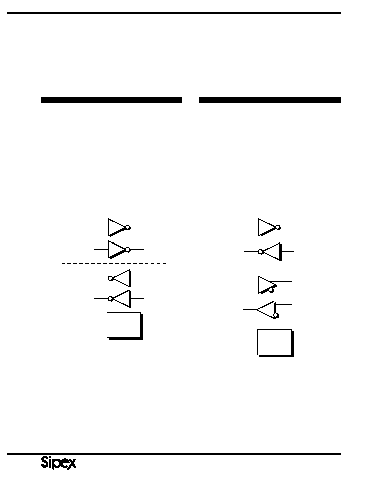
CONFIGURING THE SP301/302
Figures 3, 5 and 6 show the various combina-
tions of simultaneous RS-232 and RS-422 op-
eration that can be achieved with the SP301.
Similarly, Figures 4, 7 and 8 show the various
combinations for the SP302. Each of these con-
figurations are software selectable by logic level
on the SELECT A and SELECT B control lines.
Configuration can be changed "on-the-fly".
57
Corporation
SIGNAL PROCESSING EXCELLENCE
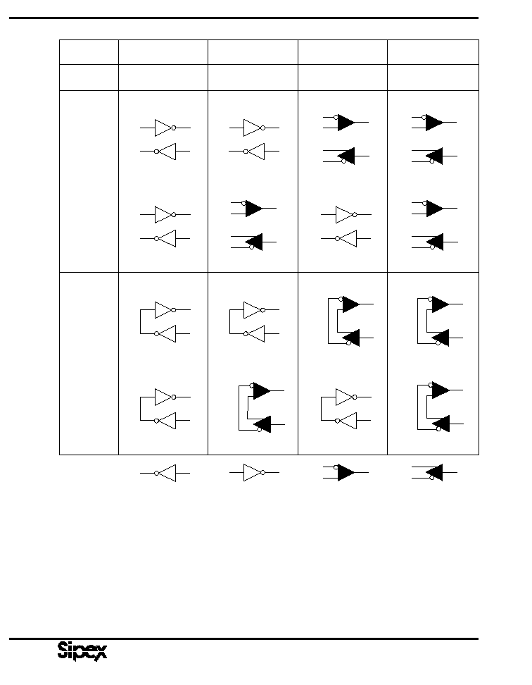
FIGURE 3: SP301 CONTROL LOGIC CONFIGURATION
RIA
1
SELECTION
SELECT A:
SELECT B:
NON
LOOPBACK
(LB = 1)
LOOPBACK
(LB=0)
ROA
RIB
1
ROB
RIB
2
ROB
RIB
1
TOB
1
TIB
TOB
2
TOA
1
TIA
TOB
1
TIB
RIA
1
ROA
TOA*
1
TIA
RIB
1
ROB
TOB*
1
TIB
RIA
1
ROA
TOA
1
TIA
RIA
1
ROA
TOA*
1
TIA
RIB
1
ROB
TOB
1
TIB
RIB
1
ROB
TOB*
1
TIB
RIA
2
ROA
RIA
1
TOA
1
TIA
TOA
2
RIA
2
ROA
RIA
1
TOA
1
TIA
TOA
2
RIB
2
ROB
RIB
1
TOB
1
TIB
TOB
2
RIA
2
ROA
RIA
1
TOA*
1
TIA
TOA*
2
RIB
2
ROB
RIB
1
TOB*
1
TIB
TOB*
2
RIB
2
ROB
RIB
1
TOB*
1
TIB
TOB*
2
RIA
2
ROA
RIA
1
TOA*
1
TIA
TOA*
2
LOGIC VALUE
1
1
LOGIC VALUE
1
0
LOGIC VALUE
0
1
LOGIC VALUE
0
0
RS-232 DRIVER
* Tristate Output
RS-232 RECEIVER
RS-422 RECEIVER
RS-422 DRIVER

Corporation
SIGNAL PROCESSING EXCELLENCE
58
FIGURE 4: SP302 CONTROL LOGIC CONFIGURATION
RIA
1
SELECTION
SELECT A:
SELECT B:
NON
LOOPBACK
(LB = 1)
LOOPBACK
(LB=0)
ROA
1
RIB
2
ROB
1
RIB
1
TOB
1
TIB
1
TOB
2
TOA
1
TIA
1
RIA
1
ROA
1
TOA
1
TIA
1
RIA
2
ROA
1
RIA
1
TOA
1
TIA
1
TOA
2
RIA
2
ROA
1
RIA
1
TOA
1
TIA
1
TOA
2
RIB
2
ROB
1
RIB
1
TOB
1
TIB
1
TOB
2
RIB
2
ROB
1
RIB
1
TOB*
1
TIB
1
TOB*
2
RIA
2
ROA
1
RIA
1
TOA*
1
TIA
1
TOA*
2
LOGIC VALUE
1
1
LOGIC VALUE
1
0
LOGIC VALUE
0
1
LOGIC VALUE
0
0
RS-232 DRIVER
* Tristate Output
RS-232 RECEIVER
RS-422 RECEIVER
RS-422 DRIVER
RIA
2
ROA
2
RIA
2
ROA
2
TOA
2
TIA
2
TOA
2
TIA
2
RIB
1
ROB
1
TOB
1
TIB
1
RIB
2
ROB
2
TOB
2
TIB
2
RIA
1
ROA
1
TOA*
1
TIA
1
RIA
2
ROA
2
TOA*
2
TIA
2
RIB
1
ROB
1
TOB
1
TIB
1
RIB
2
ROB
2
TOB
2
TIB
2
RIA
1
ROA
1
TOA*
1
TIA
1
RIA
2
ROA
2
TOA*
2
TIA
2
RIB
1
ROB
1
TOB
1
TIB
1
RIB
2
ROB
2
TOB
2
TIB
2
RIB
1
ROB
1
TOB
1
TIB
1
RIB
2
ROB
2
TOB
2
TIB
2
RIA
2
ROA
1
RIA
1
TOA*
1
TIA
1
TOA*
2
RIB
2
ROB
1
RIB
1
TOB*
1
TIB
1
TOB*
2
59
Corporation
SIGNAL PROCESSING EXCELLENCE
One-Channel Full Duplex RS-232 &
One-Channel Full Duplex RS-422
A single RS-232 line driver and receiver, and a
single RS-422 line driver and receiver.
FIGURE 5: SP301 CONFIGURATIONS
RIA
1
ROA
TOA
1
TIA
RIB
1
ROB
TOB
1
TIB
RS-232 LINE DRIVERS
RS-232 RECEIVERS
SELECT A = 0
SELECT B = 0
LB = 1
RIA
1
ROA
TOA
1
TIA
RIB
1
ROB
TOB
1
TIB
RS-232 LINE DRIVER & RECEIVER
RS-422 LINE DRIVER & RECEIVER
TOB
2
RIB
2
SELECT A = 0
SELECT B = 1
LB = 1
Two-Channel Full Duplex RS-232
Two independent channels of RS-232 line driver
and two channels of RS-232 receiver.

Corporation
SIGNAL PROCESSING EXCELLENCE
60
One-Channel Full Duplex RS-232 &
One-Channel Full Duplex RS-422
Opposite Drivers
A single RS-232 line driver and receiver, and a
single RS-422 line driver and receiver. At first
glance, this is the same configuration as that in
Figure 5. Note however that functions are acti-
vated on the opposite channels as that of those in
Figure 1b.
Two-Channel Full Duplex RS-422
Two RS-422 line drivers and two RS-422
receivers.
FIGURE 6: SP301 CONFIGURATIONS
RIA
1
ROA
TOA
1
TIA
RIB
1
ROB
TOB
1
TIB
RS-422 LINE DRIVER & RECEIVER
RS-232 LINE DRIVER & RECEIVER
TOA
2
RIA
2
SELECT A = 1
SELECT B = 0
LB = 1
RIA
1
ROA
TOA
1
TIA
RS-422 LINE DRIVERS
RS-422 RECEIVERS
SELECT A = 1
SELECT B = 1
LB = 1
TOA
2
RIA
2
RIB
1
ROB
RIB
2
TOB
1
TIB
TOB
2
61
Corporation
SIGNAL PROCESSING EXCELLENCE
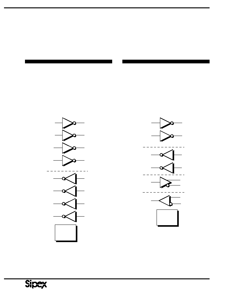
Four-Channel Duplex RS-232
Four independent channels of RS-232 line driver
and four channels of RS-232 receiver.
Two-Channel Duplex RS-232 &
One-Channel Duplex RS-422
Two RS-232 line drivers and receivers, and a
single RS-422 line driver and receiver.
FIGURE 7: SP302 CONFIGURATIONS
RIA
1
ROA
1
TOA
1
TIA
1
RIB
1
ROB
1
TOB
1
TIB
1
RS-232 LINE DRIVERS
RS-232 RECEIVERS
RIA
2
ROA
2
TOA
2
TIA
2
RIB
2
ROB
2
TOB
2
TIB
2
SELECT A = 0
SELECT B = 0
LB = 1
RIA
1
ROA
1
TOA
1
TIA
1
RIB
1
ROB
1
TOB
1
TIB
1
RS-422 LINE DRIVER
RS-422 RECEIVER
TOB
2
RIB
2
TOA
2
TIA
2
RIA
2
ROA
2
RS-232 LINE DRIVERS
RS-232 RECEIVERS
SELECT A = 0
SELECT B = 1
LB = 1
Corporation
SIGNAL PROCESSING EXCELLENCE
62
Two-Channel Duplex RS-232 &
One-Channel Duplex RS-422
Opposite Drivers
Two RS-232 line drivers and receivers, and a
single RS-422 line driver and receiver. At first
glance, this is the same configuration in Figure
7. Note however that functions are activated on
the opposite channels.
Two-Channel Duplex RS-422
Two RS-422 line drivers and two RS-422
receivers.
FIGURE 8: SP302 CONFIGURATIONS
RIA
1
ROA
1
TOA
1
TIA
1
RS-422 LINE DRIVERS
RS-422 RECEIVERS
TOA
2
RIA
2
RIB
1
ROB
1
RIB
2
TOB
1
TIB
1
TOB
2
SELECT A = 1
SELECT B = 1
LB = 1
RIB
1
ROB
1
TOB
1
TIB
1
RIA
1
ROA
1
TOA
1
TIA
1
RS-232 LINE DRIVERS
RS-232 RECEIVER
TOA
2
RIA
2
TOB
2
TIB
2
RIB
2
ROB
2
SELECT A = 1
SELECT B = 0
LB = 1
RS-422 LINE DRIVER
RS-422 RECEIVER

63
Corporation
SIGNAL PROCESSING EXCELLENCE
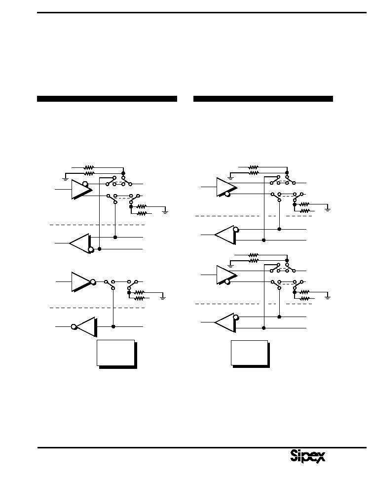
SP301 CONFIGURATIONS IN LOOPBACK MODE
Two -Channel Full Duplex RS-232
One-Channel Full Duplex RS-232 &
One-Channel Full Duplex RS-422
LOOPBACK
Both the SP301 and SP302 have a function called
loopback, which is essentially a chip self-test. How-
ever, by connecting system test loops with the inputs
and outputs of the SP301/302, a system-level diag-
nostic can be run on power-up or on command. The
RIA
1
ROA
TOA
1
TIA
RIB
1
ROB
TOB
1
TIB
RS-232 LINE DRIVERS
RS-232 RECEIVERS
SELECT A = 0
SELECT B = 0
LB = 1
RIA
1
ROA
TOA
1
TIA
RIB
1
ROB
TOB
1
TIB
TOB
2
RIB
2
SELECT A = 0
SELECT B = 1
LB = 0
(ACTIVE)
V
EE
10k
10k
V
EE
10k
10k
V
EE
10k
10k
RS-232 LINE DRIVER
RS-232 RECEIVER
RS-422 LINE DRIVER
RS-422 RECEIVER
test loops can be enabled and disabled allowing both
system test and operation with the same components.
A maximum data rate for loopback of 3kbps is
recommended. Loopback is a pin-programmable func-
tion, activated by a logic low on the LB pin (19). As
Corporation
SIGNAL PROCESSING EXCELLENCE
64
SP301 CONFIGURATIONS IN LOOPBACK MODE
One-Channel Full Duplex RS-232 &
One-Channel Full Duplex RS-422
Opposite Drivers
Two-Channel Full Duplex RS-422
shown in these figures, the loopback function
internally connects the driver outputs to the
corresponding receiver inputs, and switches the
output pin to a resistive divider of 10k
nominal
impedance from V
EE
to ground. Receiver out-
puts are left active for signal verification.
During loopback, the receiver inputs are tied to
ground via a 5k
pulldown resistor. To mini-
mize loopback errors, the receiver inputs must
be limited to
±
10V swings.
RIA
1
ROA
TOA
1
TIA
RIB
1
ROB
TOB
1
TIB
RS-232 LINE DRIVER
RS-232 RECEIVER
TOA
2
RIA
2
SELECT A = 1
SELECT B = 0
LB = 0
(ACTIVE)
V
EE
10k
10k
V
EE
10k
10k
V
EE
10k
10k
RS-422 LINE DRIVER
RS-422 RECEIVER
RS-422 LINE DRIVER
RS-422 RECEIVER
RIB
1
ROB
RIB
2
TOB
1
TIB
TOB
2
SELECT A = 1
SELECT B = 1
LB = 0
(ACTIVE)
V
EE
10k
10k
V
EE
10k
10k
RS-422 LINE DRIVER
RS-422 RECEIVER
RIA
1
ROA
RIA
2
TOA
1
TIA
TOA
2
V
EE
10k
10k
V
EE
10k
10k

65
Corporation
SIGNAL PROCESSING EXCELLENCE
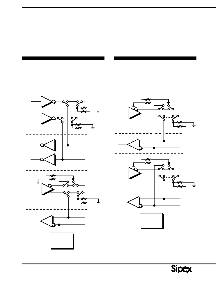
SP302 CONFIGURATIONS IN LOOPBACK MODE
Four-Channel Duplex RS-232
Two-Channel Duplex RS-232 &
One-Channel Duplex RS-422
RIA
1
ROA
1
TOA
1
TIA
1
RIB
1
ROB
1
TOB
1
TIB
1
RS-232 LINE DRIVER
RS-232 RECEIVER
SELECT A = 0
SELECT B = 0
LB = 0
(ACTIVE)
RIA
2
ROA
2
TOA
2
TIA
2
RIB
2
ROB
2
TOB
2
TIB
2
V
EE
10k
RS-232 LINE DRIVER
RS-232 RECEIVER
V
EE
10k
10k
RS-232 LINE DRIVER
RS-232 RECEIVER
V
EE
10k
10k
RS-232 LINE DRIVER
RS-232 RECEIVER
V
EE
10k
10k
10k
RIA
1
ROA
1
TOA
1
TIA
1
RIB
1
ROB
1
TOB
1
TIB
1
RS-232 LINE DRIVER
RS-232 RECEIVER
SELECT A = 0
SELECT B = 1
LB = 0
(ACTIVE)
TOB
2
RIB
2
TOA
2
TIA
2
RIA
2
ROA
2
RS-422 LINE DRIVER
RS-422 RECEIVER
V
EE
10k
10k
V
EE
10k
10k
RS-232 LINE DRIVER
RS-232 RECEIVER
V
EE
10k
10k
V
EE
10k
10 k
Corporation
SIGNAL PROCESSING EXCELLENCE
66
SP302 CONFIGURATIONS IN LOOPBACK MODE
Two-Channel Duplex RS-232 &
One-Channel Duplex RS-422
Opposite Drivers
Two-Channel Duplex RS-422
RIB
1
ROB
1
TOB
1
TIB
1
RIA
1
ROA
1
TOA
1
TIA
1
RS-232 LINE DRIVERS
RS-232 RECEIVERS
SELECT A = 1
SELECT B = 0
LB = 0
(ACTIVE)
TOA
2
RIA
2
TOB
2
TIB
2
RIB
2
ROB
2
RS-422 LINE DRIVER
RS-422 RECEIVER
V
EE
10k
10k
V
EE
10k
10k
V
EE
10k
10k
V
EE
10k
10k
RIA
1
ROA
1
TOA
1
TIA
1
RS-422 LINE DRIVERS
RS-422 RECEIVERS
SELECT A = 1
SELECT B = 1
LB = 0
(ACTIVE)
TOA
2
RIA
2
RIB
1
ROB
1
RIB
2
TOB
1
TIB
1
TOB
2
V
EE
10k
10k
V
EE
10k
10k
V
EE
10k
10k
V
EE
10k
10k
RS-422 LINE DRIVERS
RS-422 RECEIVERS

67
Corporation
SIGNAL PROCESSING EXCELLENCE
ORDERING INFORMATION
Max # of Duplex Channels
Model
RS232
RS422
Temperature
Package
SP301CS .......... 2 ........................ 2 ............. 0
°
C to +70
°
C .......................... 24-pin singlewidth plastic DIP
SP301CT .......... 2 ........................ 2 ............. 0
°
C to +70
°
C ........................................................ 28-pin SOIC
SP301ES .......... 2 ........................ 2 ......... -40
°
C to +85
°
C .......................... 24-pin singlewidth plastic DIP
SP301ET .......... 2 ........................ 2 ......... -40
°
C to +85
°
C ........................................................ 28-pin SOIC
SP302CS .......... 4 ........................ 2 ............. 0
°
C to +70
°
C .......................... 24-pin singlewidth plastic DIP
SP302CT .......... 4 ........................ 2 ............. 0
°
C to +70
°
C ........................................................ 28-pin SOIC
SP302ES .......... 4 ........................ 2 ......... -40
°
C to +85
°
C .......................... 24-pin singlewidth plastic DIP
SP302ET .......... 4 ........................ 2 ......... -40
°
C to +85
°
C ........................................................ 28-pin SOIC

Corporation
SIGNAL PROCESSING EXCELLENCE
68
THIS PAGE LEFT INTENTIONALLY BLANK