
1
Date: 6/2/04
SP3223EB/3243EB +3.0V to +5.5V RS-232 Transceivers
© Copyright 2004 Sipex Corporation
SP3223EB/3243EB
Intelligent +3.0V to +5.5V RS-232 Transceivers
The SP3223EB and SP3243EB products are RS-232 transceiver solutions intended for
portable or hand-held applications such as notebook and palmtop computers. The SP3223EB
and SP3243EB use an internal high-efficiency, charge-pump power supply that requires only
0.1µF capacitors in 3.3V operation. This charge pump and Sipex's driver architecture allow
the SP3223EB/3243EB series to deliver compliant RS-232 performance from a single power
supply ranging from +3.0V to +5.5V. The SP3223EB is a 2-driver/2-receiver device, and the
SP3243EB is a 3-driver/5-receiver device ideal for laptop/notebook computer and PDA
applications. The SP3243EB includes one complementary receiver that remains alert to
monitor an external device's Ring Indicate signal while the device is shutdown.
The AUTO ON-LINEÆ feature allows the device to automatically "wake-up" during a shutdown
state when an RS-232 cable is connected and a connected peripheral is turned on. Otherwise,
the device automatically shuts itself down drawing less than 1µA.
Meets true EIA/TIA-232-F Standards
from a +3.0V to +5.5V power supply
Interoperable with EIA/TIA-232 and
adheres to EIA/TIA-562 down to a +2.7V
power source
AUTO ON-LINE
Æ
circuitry automatically
wakes up from a 1µA shutdown
Minimum 250kbps data rate under load
Regulated Charge Pump Yields Stable
RS-232 Outputs Regardless of V
CC
Variations
Enhanced ESD Specifications:
+15kV Human Body Model
+15kV IEC1000-4-2 Air Discharge
+8kV IEC1000-4-2 Contact Discharge
DESCRIPTION
SELECTION TABLE
Applicable U.S. Patents - 5,306,954; and other patents pending.
e
c
i
v
e
D
s
e
il
p
p
u
S
r
e
w
o
P
2
3
2
-
S
R
s
r
e
v
i
r
D
2
3
2
-
S
R
s
r
e
v
i
e
c
e
R
l
a
n
r
e
t
x
E
s
t
n
e
n
o
p
m
o
C
E
N
I
L
-
N
O
O
T
U
A
Æ
y
r
t
i
u
c
r
i
C
e
t
a
t
S
-
3
L
T
T
f
o
.
o
N
s
n
i
P
B
E
3
2
2
3
P
S
V
5
.
5
+
o
t
V
0
.
3
+
2
2
s
r
o
t
i
c
a
p
a
c
4
S
E
Y
S
E
Y
0
2
B
E
3
4
2
3
P
S
V
5
.
5
+
o
t
V
0
.
3
+
3
5
s
r
o
t
i
c
a
p
a
c
4
S
E
Y
S
E
Y
8
2
Æ
V-
1
2
3
4
17
18
19
20
5
6
7
16
15
14
SHUTDOWN
C1+
V+
C1-
C2+
C2-
ONLINE
EN
R
1
IN
GND
V
CC
T
1
OUT
STATUS
8
9
10
11
12
13
R
2
IN
R
2
OUT
SP3223EB
T
2
OUT
T
1
IN
T
2
IN
R
1
OUT
Now Available in Lead Free Packaging

Date: 6/2/04
SP3223EB/3243EB +3.0V to +5.5V RS-232 Transceivers
© Copyright 2004 Sipex Corporation
2
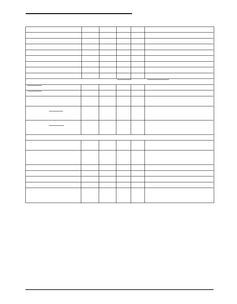
PARAMETER
MIN.
TYP.
MAX. UNITS CONDITIONS
DC CHARACTERISTICS
Supply Current,
1.0
10
µA
All RxIN open, ONLINE = GND,
AUTO ON-LINE
Æ
SHUTDOWN = V
CC
, TxIN = V
CC
or
GND,V
CC
= +3.3V, T
AMB
= +25∞C
Supply Current, Shutdown
1.0
10
µA
SHUTDOWN = GND,
V
CC
= +3.3V, T
AMB
= +25∞C,
TxIN = V
CC
or GND
Supply Current,
0.3
1.0
mA
ONLINE = SHUTDOWN = V
CC
,
AUTO ON-LINE
Æ
Disabled
TxIN = V
CC
or GND,
no load, V
CC
= +3.3V, T
AMB
= +25∞C
LOGIC INPUTS AND RECEIVER OUTPUTS
Input Logic Threshold
V
CC
= +3.3V or +5.0V, TxIN,
LOW
GND
0.8
V
EN (SP3223EB), ONLINE,
HIGH
2.4
VCC
V
SHUTDOWN
Input Leakage Current
±0.01
±1.0
µA
TxIN, EN (SP3223EB), ONLINE,
SHUTDOWN,
T
AMB
= +25∞C, V
IN
= 0V to V
CC
Output Leakage Current
±0.05
±10
µA
Receivers disabled, V
OUT
= 0V to
V
CC
Output Voltage LOW
0.4
V
I
OUT
= 1.6mA
Output Voltage HIGH
V
CC
- 0.6
V
CC
- 0.1
V
I
OUT
= -1.0mA
DRIVER OUTPUTS
Output Voltage Swing
±5.0
±5.4
V
All driver outputs loaded with 3K
to GND, T
AMB
= +25∞C
Output Resistance
300
V
CC
= V+ = V- = 0V, V
OUT
= ±2V
Output Short-Circuit Current
±35
±60
mA
V
OUT
= 0V
Output Leakage Current
±25
µA
V
CC
= 0V or 3.0V to 5.5V,
V
OUT
= ±12V, Drivers disabled
NOTE 1: V+ and V- can have maximum magnitudes of 7V, but their absolute difference cannot exceed 13V.
ABSOLUTE MAXIMUM RATINGS
These are stress ratings only and functional operation
of the device at these ratings or any other above those
indicated in the operation sections of the specifications
below is not implied. Exposure to absolute maximum
rating conditions for extended periods of time may
affect reliability and cause permanent damage to the
device.
V
CC
...................................................... -0.3V to +6.0V
V+ (NOTE 1) ...................................... -0.3V to +7.0V
V- (NOTE 1) ....................................... +0.3V to -7.0V
V+ + |V-| (NOTE 1) ........................................... +13V
I
CC
(DC V
CC
or GND current) ......................... +100mA
Input Voltages
TxIN, ONLINE,
SHUTDOWN, EN (SP3223E) ............ -0.3V to +6.0V
RxIN .................................................................. +25V
Output Voltages
TxOUT ........................................................... +13.2V
RxOUT, STATUS ..................... -0.3V to (V
CC
+ 0.3V)
Unless otherwise noted, the following specifications apply for V
CC
= +3.0V to +5.5V with T
AMB
= T
MIN
to T
MAX
,
C1 - 4 = 0.1
µF. Typical values apply at V
CC
= +3.3V or +5.0V and T
AMB
= 25
∞C.
ELECTRICAL CHARACTERISTICS
Short-Circuit Duration
TxOUT .................................................... Continuous
Storage Temperature ...................... -65∞C to +150∞C
Power Dissipation per package
28-pin PDIP
(derate 16.0mW/∞C above+70∞C) ...................... 1300mW
20-pin SSOP
(derate 9.25mW/∞C above +70∞C) ...................... 750mW
20-pin TSSOP
(derate 11.1mW/∞C above +70∞C) ....................... 900mW
28-pin SOIC
(derate 12.7mW/∞C above +70∞C) .................... 1000mW
28-pin SSOP
(derate 11.2mW/∞C above +70∞C) ...................... 900mW
28-pin TSSOP
(derate 11.1mW/∞C above +70∞C) ....................... 900mW
32-pin QFN
3
Date: 6/2/04
SP3223EB/3243EB +3.0V to +5.5V RS-232 Transceivers
© Copyright 2004 Sipex Corporation
ELECTRICAL CHARACTERISTICS
Unless otherwise noted, the following specifications apply for V
CC
= +3.0V to +5.5V with T
AMB
= T
MIN
to T
MAX
,
C1 - 4 = 0.1
µF. Typical values apply at V
CC
= +3.3V or +5.0V and T
AMB
= 25
∞C.
PARAMETER
MIN.
TYP.
MAX. UNITS CONDITIONS
RECEIVER INPUTS
Input Voltage Range
-25
25
V
Input Threshold LOW
0.6
1.2
V
V
CC
= 3.3V
Input Threshold LOW
0.8
1.5
V
V
CC
= 5.0V
Input Threshold HIGH
1.5
2.4
V
V
CC
= 3.3V
Input Threshold HIGH
1.8
2.4
V
V
CC
= 5.0V
Input Hysteresis
0.3
V
Input Resistance
3
5
7
k
AUTO ON-LINE
Æ
CIRCUITRY CHARACTERISTICS (ONLINE = GND, SHUTDOWN = V
CC
)
STATUS Output Voltage LOW
0.4
V
I
OUT
= 1.6mA
STATUS Output Voltage HIGH
V
CC
- 0.6
V
I
OUT
= -1.0mA
Receiver Threshold to Drivers
Enabled (t
ONLINE
)
200
µs
Figure 20
Receiver Positive or Negative
0.5
µs
Figure 20
Threshold to STATUS HIGH
(t
STSH
)
Receiver Positive or Negative
20
µs
Figure 20
Threshold to STATUS LOW
(t
STSL
)
TIMING CHARACTERISTICS
Maximum Data Rate
250
kbps
R
L
= 3K, C
L
= 1000pF,
one driver active
Receiver Propagation Delay
t
PHL
0.15
µs
Receiver input to Receiver output,
t
PLH
0.15
C
L
= 150pF
Receiver Output Enable Time
200
ns
Normal operation
Receiver Output Disable Time
200
ns
Normal operation
Driver Skew
100
ns
| t
PHL
- t
PLH
|, T
AMB
= 25∞C
Receiver Skew
50
ns
| t
PHL
- t
PLH
|
Transition-Region Slew Rate
30
V/µs
V
CC
= 3.3V, R
L
= 3K, T
AMB
= 25∞C,
measurements taken from -3.0V to
+3.0V or +3.0V to -3.0V

Date: 6/2/04
SP3223EB/3243EB +3.0V to +5.5V RS-232 Transceivers
© Copyright 2004 Sipex Corporation
4
Figure 1. Transmitter Output Voltage VS. Load
Capacitance for the SP3223EB
Figure 2. Slew Rate VS. Load Capacitance for the
SP3223EB
TYPICAL PERFORMANCE CHARACTERISTICS
Unless otherwise noted, the following performance characteristics apply for V
CC
= +3.3V, 250kbps data rate, all drivers
loaded with 3K
, 0.1µF charge pump capacitors, and T
AMB
= +25
∞C.
30
25
20
15
10
5
0
0
500
1000
2000
3000
4000
5000
Slew rate (V/
µ
s)
Load Capacitance (pF)
- Slew
+ Slew
1 Transmitter at 250Kbps
1 Transmitter at 15.6Kbps
All drivers loaded 3K + Load Cap
35
30
25
20
15
10
5
0
I
CC
(mA)
Load Capacitance (pF)
0
1000
2000
3000
4000
5000
250Kbps
125Kbps
20Kbps
1 Transmitter at 250Kbps
1 Transmitter at 15.6Kbps
All drivers loaded 3K + Load Cap
Figure 3. Supply Current VS. Load Capacitance when
Transmitting Data for the SP3223EB
Figure 4. Supply Current VS. Supply Voltage for
the SP3243EB
20
15
10
5
0
2.7
3
3.5
4
4.5
5
Supply Voltage (V
DC
)
Supply Current (mA)
1 Transmitter at 250Kbps
2 Transmitters at 15.6Kbps
All drivers loaded with 3K // 1000pF
Figure 5. Transmitter Output Voltage VS. Supply
Voltage for the SP3243EB
Figure 6. Transmitter Output Voltage VS. Load
Capacitance for the SP3243EB
6
4
2
0
-2
-4
-6
0
1000
2000
3000
4000
5000
TxOUT +
TxOUT -
T
ransmitter Output
V
oltage (V
DC
)
Load Capacitance (pF)
6
4
2
0
-2
-4
-6
0
1000
2000
3000
4000
5000
TxOUT +
TxOUT -
T
ransmitter Output
V
oltage (V)
Load Capacitance (pF)
6
4
2
0
-2
-4
-6
2.7
3
3.5
4
4.5
5
Supply Voltage (V
DC
)
T
ransmitter Output
V
oltage (V
DC
)
TxOUT -
TxOUT +

5
Date: 6/2/04
SP3223EB/3243EB +3.0V to +5.5V RS-232 Transceivers
© Copyright 2004 Sipex Corporation
TYPICAL PERFORMANCE CHARACTERISTICS
Unless otherwise noted, the following performance characteristics apply for V
CC
= +3.3V, 250kbps data rate, all drivers
loaded with 3K
, 0.1µF charge pump capacitors, and T
AMB
= +25
∞C.
Figure 7. Slew Rate VS. Load Capacitance for the
SP3243EB
25
20
15
10
5
0
0
500
1000
2000
3000
4000
5000
Slew rate (V/
µ
s)
Load Capacitance (pF)
- Slew
+ Slew
1 Transmitter at 250Kbps
2 Transmitter at 15.6Kbps
All drivers loaded 3K + Load Cap
Figure 8. Supply Current VS. Load Capacitance when
Transmitting Data for the SP3243EB
40
35
30
25
20
15
10
5
0
Supply Current
(mA)
Load Capacitance (pF)
0
1000
2000
3000
4000
5000
250Kbps
120Kbps
20Kbps
1 Transmitter at full Data Rate
2 Transmitters at 15.5 Kbps
All Transmitters loades 3K + Load Cap
6
4
2
0
-2
-4
-6
2.7
3
3.5
4
4.5
5
Supply Voltage (V
DC
)
T
ransmitter Output
V
oltage (V)
TxOUT -
TxOUT +
Figure 9. Supply Current VS. Supply Voltage for the
SP3243EB
Figure 10. Transmitter Output Voltage VS. Supply
Voltage for the SP3243EB
25
20
15
10
5
0
2.7
3
3.5
4
4.5
5
Supply Voltage (V
DC
)
Supply Current (mA)
1 Transmitter at 250Kbps
2 Transmitters at 15.6Kbps
All drivers loaded with 3K // 1000pF