 | –≠–ª–µ–∫—Ç—Ä–æ–Ω–Ω—ã–π –∫–æ–º–ø–æ–Ω–µ–Ω—Ç: SP331CT | –°–∫–∞—á–∞—Ç—å:  PDF PDF  ZIP ZIP |

SP331DS/13
SP331 RS-232/RS-485 Serial Transceiver
© Copyright 2000 Sipex Corporation
1
s
+5V Only Operation
s
Software Programmable RS-232 or
RS-485 Selection
s
Four RS-232 Transceivers in RS-232
Mode
s
Two RS-485 Full-Duplex Transceivers
in RS-485 Mode
s
Two RS-232 Transceivers and One
RS-485 Transceiver in Dual Mode
s
Self-Testing Loopback Mode
s
Full Driver Tri-State (Hi-Z) Control
s
Ideal for RS-232 to RS-485 conversion
DESCRIPTION...
The SP331 is a programmable RS-232 and/or RS-485 transceiver IC. The SP331 contains four
drivers and four receivers when selected in RS-232 mode; and two drivers and two receivers
when selected in RS-485 mode. The SP331 also contains a dual mode which has two RS-232
drivers/receivers plus one differential RS-485 driver/receiver.
The RS-232 transceivers can typically operate at 230kbps while adhering to the RS-232
specifications. The RS-485 transceivers can operate up to 10Mbps while adhering to the RS-485
specifications. The SP331 includes a self-test loopback mode where the driver outputs are
internally configured to the receiver inputs. This allows for easy diagnostic serial port testing
without using an external loopback plug. The RS-232 and RS-485 drivers can be disabled
(High-Z output) by controlling a set of four select pins.
TI4
SEL_B
TX4
TX3
VCC
TX1
TX2
GND
C1+
V+ (VDD)
C2+
C1≠
C2≠
V≠ (VSS)
TI3
TI2
TI1
SEL_C
SEL_A
SEL_D
RX4
RX3
RX2
RX1
RI4
RI3
RI2
RI1
28
27
26
25
24
23
22
21
20
19
18
17
16
15
1
2
3
4
5
6
7
8
9
10
11
12
13
14
SP331
SP331
Programmable RS-232/RS-485 Transceiver
Æ

SP331DS/13
SP331 RS-232/RS-485 Serial Transceiver
© Copyright 2000 Sipex Corporation
2
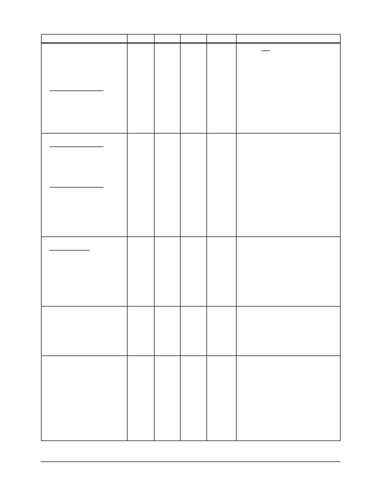
SPECIFICATIONS
Typically 25
∞
C @ Vcc = +5V unless otherwise noted.
MIN.
TYP.
MAX.
UNITS
CONDITIONS
LOGIC INPUTS
V
IL
0.8
Volts
V
IH
2.0
Volts
LOGIC OUTPUTS
V
OL
0.4
Volts
I
OUT
= -3.2mA
V
OH
2.4
Volts
I
OUT
= 1.0mA
RS-232 DRIVER
DC Characteristics
HIGH Level Output
+5.0
+15
Volts
R
L
=3k
, V
IN
=0.8V
LOW Level Output
≠15.0
≠5.0
Volts
R
L
=3k
, V
IN
=2.0V
Open Circuit Voltage
≠15
+15
Volts
Short Circuit Current
±
100
mA
V
OUT
= 0V
Power Off Impedance
300
V
cc
= 0V, V
out
=
±
2.0V
AC Characteristics
Slew Rate
30
V/
µ
s
R
L
=3k
, C
L
= 50pF
V
CC
= +5.0V, T
A
@ +25
∞
C
Transition Time
1.5
µ
s
R
L
=3k
, C
L
=2500pF ;
between
±
3V, T
A
@ +25
∞
C
Maximum Data Rate
120
235
kbps
R
L
=3k
, C
L
=2500pF
Propagation Delay
t
PHL
2
8
µ
s
Measured from 1.5V of V
IN
t
PLH
2
8
µ
s
to 50% of V
OUT
;
R
L
=3k
RS-232 RECEIVER
DC Characteristics
HIGH Threshold
1.7
3.0
Volts
LOW Threshold
0.8
1.2
Volts
Receiver Open Circuit Bias
+2.0
Volts
Input Impedance
3
5
7
k
V
IN
= +15V to ≠15V
AC Characteristics
Maximum Data Rate
120
235
kbps
Propagation Delay
t
PHL
0.25
1
µ
s
Measured from 50% of V
IN
t
PLH
0.25
1
µ
s
to 1.5V of V
OUT
.
RS-485 DRIVER
DC Characteristics
Open Circuit Voltage
6.0
Volts
Differential Output
1.5
5.0
Volts
R
L
=54
, C
L
=50pF
ABSOLUTE MAXIMUM RATINGS
These are stress ratings only and functional operation
of the device at these ratings or any other above those
indicated in the operation sections of the specifications
below is not implied. Exposure to absolute maximum
rating conditions for extended periods of time may
affect reliability.
V
CC
...........................................................................+7V
Storage Temperature..........................-65∞C to +150∞C
Power Dissipation
28-pin Plastic DIP...........................1000mW
28-pin Plastic SOIC.......................1000mW
Package Derating:
28-pin Plastic DIP
¯
JA
....................................................40
∞
C/W
28-pin Plastic SOIC
¯
JA
....................................................40
∞
C/W
SP331DS/13
SP331 RS-232/RS-485 Serial Transceiver
© Copyright 2000 Sipex Corporation
3
SPECIFICATIONS
Typically 25
∞
C @ Vcc = +5V unless otherwise noted.
MIN.
TYP.
MAX.
UNITS
CONDITIONS
RS-485 DRIVER
Balance
±
0.2
Volts
|V
T
| - |V
T
|
Common-Mode Output
3.0
Volts
Output Current
28.0
mA
R
L
=54
Short Circuit Current
±
250
mA
Terminated in ≠7V to +10V
AC Characteristics
Maximum Data Rate
10
Mbps
R
L
=54
Output Transition Time
30
50
ns
Rise/fall time, 10%≠90%
Propagation Delay
See Figures 2 & 4
t
PHL
80
120
ns
R
DIFF
=54
, C
L1
=C
L2
=100pF
t
PLH
80
120
ns
R
DIFF
=54
, C
L1
=C
L2
=100pF
Driver Output Skew
10
20
ns
per Figure 4, t
SKEW
= | t
DPLH
- t
DPHL
|
RS-485 RECEIVER
DC Characteristics
Inputs
Common Mode Range
≠7.0
+12.0
Volts
Receiver Sensitivity
±
0.2
±
0.3
Volts
≠7V
V
CM
+12V
Input Impedance
12
15
k
≠7V
V
CM
+12V
AC Characteristics
Maximum Data Rate
10
Mbps
Propagation Delay
See Figures 2 & 6
t
PHL
130
200
ns
R
DIFF
=54
, C
L1
=C
L2
=100pF
t
PLH
130
200
ns
R
DIFF
=54
, C
L1
=C
L2
=100pF
Differential Receiver Skew
10
20
ns
t
SKEW
= | t
PLH
≠ t
PHL
|; R
DIFF
=54
,
C
L1
=C
L2
=100pF
ENABLE TIMING
RS-485 Driver
Enable Time
See Figures 3 & 5
Enable to Low
90
150
ns
C
L
=15pF, S
1
Closed
Enable to High
90
150
ns
C
L
=15pF, S
2
Closed
Disable Time
See Figures 3 & 5
Disable From Low
80
120
ns
C
L
=15pF, S
1
Closed
Disable From High
80
120
ns
C
L
=15pF, S
2
Closed
POWER REQUIREMENTS
Supply Voltage V
CC
+4.75
+5.25
Volts
Supply Current I
CC
No Load (T
x
Disabled)
10
15
mA
SEL_A
≤
SEL_D = "0001"
No Load (RS-232 Mode)
15
30
mA
SEL_A
≤
SEL_D = "0000"
No Load (RS-485 Mode)
7
20
mA
SEL_A
≤
SEL_D = "1100"
ENVIRONMENTAL
Operating Temperature
Commercial (..C..)
0
+70
∞
C
Industrial (..E..)
≠40
+85
∞
C
Storage Temperature
≠65
+150
∞
C

SP331DS/13
SP331 RS-232/RS-485 Serial Transceiver
© Copyright 2000 Sipex Corporation
4
Figure 2. Driver/Receiver Timing Test Circuit
Figure 3. Driver Timing Test Load #2 Circuit
Figure 1. Driver DC Test Load Circuit
C
L1
15pF
RO
A
B
A
B
DI
C
L2
R
L
A
B
R
R
V
OD
V
OC
500
C
L
Output
Under
Test
S
1
S
2
V
CC
TEST CIRCUITS
RECEIVER INPUT GRAPH
+1.0mA
≠0.6mA
+12V
+6V
≠3V
≠7V
1 Unit Load
Maximum Input Current
versus Voltage
RS-485 RECEIVER

SP331DS/13
SP331 RS-232/RS-485 Serial Transceiver
© Copyright 2000 Sipex Corporation
5
Figure 5. Driver Enable and Disable Times
Figure 6. Receiver Propagation Delays
V
OH
V
OL
RECEIVER OUT
1.5V
1.5V
t
PHL
f = 1MHz; t
R
10ns; t
F
10ns
OUTPUT
V
0D2
+
V
0D2
≠
A ≠ B
0V
0V
t
PLH
INPUT
Figure 4. Driver Propagation Delays
SWITCHING WAVEFORMS
+3V
0V
DE
5V
V
OL
A, B
0V
1.5V
1.5V
t
ZL
t
ZH
f = 1MHz; t
R
< 10ns; t
F
< 10ns
V
OH
A, B
2.3V
2.3V
t
LZ
t
HZ
0.5V
0.5V
Output normally LOW
Output normally HIGH
+3V
0V
DRIVER INPUT
A
B
DRIVER
OUTPUT
V
O
+
DIFFERENTIAL
OUTPUT
V
A
≠ V
B
0V
V
O
≠
1.5V
1.5V
t
PLH
t
F
t
R
f
1MHz; t
R
10ns; t
F
10ns
V
O
1/2V
O
1/2V
O
t
PHL
t
SKEW
= |t
DPLH
- t
DPHL
|
t
DPLH
t
DPHL