 | –≠–ª–µ–∫—Ç—Ä–æ–Ω–Ω—ã–π –∫–æ–º–ø–æ–Ω–µ–Ω—Ç: SP432 | –°–∫–∞—á–∞—Ç—å:  PDF PDF  ZIP ZIP |

1
SP432DS/10 SP432 High Speed, Low Power Quad Differential Line Receiver © Copyright 1997 Sipex Corporation
SP432
High Speed, Low Power Quad RS-422
Differential Line Receiver
The SP432 is a quad differential line receiver designed to meet the specifications of
RS-422. The SP432 features Sipex's BiCMOS process allowing low power operational
characteristics of CMOS technology while meeting all of the demands of the RS-422 serial
protocol over 50Mbps under load. The RS-422 protocol allows up to 10 receivers to be
connected to a multipoint bus transmission line. The SP432 features a receiver enable
control common to all four receivers and a tri-state output with 6mA source and sink
capability. Since the cabling can be as long as 4,000 feet, the RS-422 receivers of the SP432
are equipped with a wide (-7.0V to +7.0V) common-mode input voltage range to accomodate
ground potential differences.
s
Compatible with the EIA standard for
RS-422 serial protocol
s
Quad Differential Line Receivers
s
Tri-state Output Control
s
8ns Typical Receiver Propagation Delays
s
60mV Typical Input Hysteresis
s
Single +3.3V to +5V Supply Operation
s
Common Receiver Enable Control
s
Compatibility with the industry standard
26LV32 and 26C32
s
-7.0V to +7.0V Common-Mode Input
Voltage Range
DESCRIPTION
RI
4
A RI
4
B
V
CC
GND
R04
R02
R03
R01
INPUTS
OUTPUTS
ENABLE
ENABLE
RI
3
A RI
3
B
RI
2
A RI
2
B
RI
1
A RI
1
B
V
CC
RI2B
1
2
3
4
13
14
5
6
7
RI3A
RI1A
R01
ENABLE
R02
RI2A
R03
RI1B
ENABLE
R04
RI4A
RI4B
8
9
GND
RI3B
10
12
11
15
16
SP432
SIGNAL PROCESSING EXCELLENCE

2
SP432DS/10 SP432 High Speed, Low Power Quad Differential Line Receiver © Copyright 1997 Sipex Corporation
ABSOLUTE MAXIMUM RATINGS
These are stress ratings only and functional operation of the device at
these ratings or any other above those indicated in the operation sections
of the specifications below is not implied. Exposure to absolute maximum
rating conditions for extended periods of time may affect reliability and
cause permanent damage to the device.
V
CC
(SupplyVoltage).......................................................................+7.0V
V
CM
(Common Mode Range)...........................................................
±
14V
V
DIFF
(Differential Input Voltage)......................................................
±
14V
V
IN
(Enable Input Voltage)..............................................................+7.0V
T
STG
(Storage Temperature Range)..............................-65
∞
C to +150
∞
C
Lead Temperature (4sec)............................................................+260
∞
C
Maximum Current Per Output......................................................
±
25mA
Storage Temperature....................................................-65
∞
C to +150
∞
C
Power Dissipation Per Package
16-pin PDIP (derate 14.3mW/
o
C above +70
o
C)........................1150mW
16-pin NSOIC (derate 8.95mW/
o
C above +70
o
C).......................725mW
Figure 1. SP432 Block Diagram
ESD
RI
4
A RI
4
B
V
CC
GND
R04
R02
R03
R01
INPUTS
OUTPUTS
ENABLE
ENABLE
RI
3
A RI
3
B
RI
2
A RI
2
B
RI
1
A RI
1
B

3
SP432DS/10 SP432 High Speed, Low Power Quad Differential Line Receiver © Copyright 1997 Sipex Corporation
S
R
E
T
E
M
A
R
A
P
C
D
.
N
I
M
.
P
Y
T
.
X
A
M
S
T
I
N
U
S
N
O
I
T
I
D
N
O
C
,
e
g
a
t
l
o
V
y
l
p
p
u
S
V
C
C
0
.
3
5
.
5
V
s
e
m
i
T
ll
a
F
r
o
e
s
i
R
t
u
p
n
I
e
l
b
a
n
E
3
s
n
s
c
i
t
s
i
r
e
t
c
a
r
a
h
C
l
a
c
i
r
t
c
e
l
E
t
u
p
n
I
V
,
e
g
a
t
l
o
V
t
u
p
n
I
l
a
i
t
n
e
r
e
f
f
i
D
m
u
m
i
n
i
M
H
T
0
0
2
-
5
3
0
0
2
+
V
m
V
T
U
O
V
=
H
O
V
r
o
L
O
,
V
<
V
7
-
M
C
V
7
+
<
R
,
e
c
n
a
t
s
i
s
e
R
t
u
p
n
I
N
I
0
.
5
8
0
1
K
V
N
I
,
V
7
+
,
V
7
-
=
D
N
G
=
t
u
p
n
i
r
e
h
t
o
t
n
e
r
r
u
C
t
u
p
n
I
I
N
I
5
2
.
1
+
5
.
1
+
A
m
V
N
I
D
N
G
=
t
u
p
n
i
r
e
h
t
o
,
V
0
1
+
=
I
N
I
5
.
1
-
5
.
2
-
A
m
V
N
I
D
N
G
=
t
u
p
n
i
r
e
h
t
o
,
V
0
1
-
=
V
,
e
g
a
t
l
o
V
l
e
v
e
L
t
u
p
n
I
H
G
I
H
e
l
b
a
n
E
m
u
m
i
n
i
M
H
I
0
.
2
V
V
,
e
g
a
t
l
o
V
l
e
v
e
L
t
u
p
n
I
W
O
L
e
l
b
a
n
E
m
u
m
i
x
a
M
L
I
8
.
0
V
I
,
t
n
e
r
r
u
C
t
u
p
n
I
e
l
b
a
n
E
m
u
m
i
x
a
M
I
0
.
1
±
µ
A
V
N
I
V
=
C
C
D
N
G
r
o
V
,
s
i
s
e
r
e
t
s
y
H
t
u
p
n
I
T
S
Y
H
0
6
V
m
V
M
C
V
0
=
,
t
n
e
r
r
u
C
y
l
p
p
u
S
t
n
e
c
s
e
i
u
Q
I
C
C
8
D
B
T
A
m
V
C
C
V
,
V
0
.
5
+
=
F
I
D
V
1
+
=
I
,
t
n
e
r
r
u
C
y
l
p
p
u
S
t
n
e
c
s
e
i
u
Q
C
C
D
B
T
A
m
V
C
C
V
3
.
3
+
=
s
c
i
t
s
i
r
e
t
c
a
r
a
h
C
l
a
c
i
r
t
c
e
l
E
t
u
p
t
u
O
V
,
e
g
a
t
l
o
V
t
u
p
t
u
O
l
e
v
e
L
h
g
i
H
m
u
m
i
n
i
M
H
O
7
.
2
D
B
T
V
V
C
C
V
,
V
0
.
3
+
=
F
F
I
D
,
V
1
+
=
I
T
U
O
A
m
0
.
6
-
=
V
,
e
g
a
t
l
o
V
t
u
p
t
u
O
l
e
v
e
L
w
o
L
m
u
m
i
x
a
M
L
O
2
.
0
3
.
0
V
V
C
C
V
,
V
0
.
5
+
=
F
F
I
D
,
V
1
-
=
I
T
U
O
A
m
0
.
6
-
=
I
,
t
n
e
r
r
u
C
e
g
a
k
a
e
L
t
u
p
t
u
O
e
t
a
t
s
-
i
r
T
m
u
m
i
x
a
M
Z
O
5
.
0
±
0
.
5
±
µ
A
V
T
U
O
V
=
C
C
,
D
N
G
r
o
V
=
E
L
B
A
N
E
L
I
V
=
E
L
B
A
N
E
,
H
I
SPECIFICATIONS
Unless otherwise noted, the following specifications apply for V
CC
= +3.0V to +5.5V with T
amb
= 25
∞
C and all MIN
and MAX limits apply across the recommended operating temperature range.

4
SP432DS/10 SP432 High Speed, Low Power Quad Differential Line Receiver © Copyright 1997 Sipex Corporation
SPECIFICATIONS (continued)
Unless otherwise noted, the following specifications apply for V
CC
= +3.0V to +5.5V, T
amb
= 25
∞
C, t
r
< 6ns, t
f
< 6ns,
and all MIN and MAX limits apply across the recommended operating temperature range.
.
N
I
M
.
P
Y
T
.
X
A
M
S
T
I
N
U
S
N
O
I
T
I
D
N
O
C
S
R
E
T
E
M
A
R
A
P
C
A
,
t
u
p
t
u
O
o
t
t
u
p
n
I
s
y
a
l
e
D
n
o
i
t
a
g
a
p
o
r
P
t
H
L
P
t
,
L
H
P
7
D
B
T
s
n
C
L
V
,
F
p
0
5
=
F
F
I
D
V
,
V
5
.
2
=
M
C
,
V
0
=
V
C
C
V
5
+
=
,
s
e
m
i
T
ll
a
F
d
n
a
e
s
i
R
t
u
p
t
u
O
t
E
S
I
R
t
,
L
L
A
F
5
D
B
T
s
n
C
L
V
,
F
p
0
5
=
F
F
I
D
V
,
V
5
.
2
=
M
C
,
V
0
=
V
C
C
V
5
+
=
,
t
u
p
t
u
O
o
t
E
L
B
A
N
E
y
a
l
e
D
n
o
i
t
a
g
a
p
o
r
P
t
Z
L
P
t
,
Z
H
P
0
1
D
B
T
s
n
C
L
R
,
F
p
0
5
=
L
0
0
0
1
=
V
,
F
F
I
D
,
V
5
.
2
=
V
C
C
V
5
+
=
,
t
u
p
t
u
O
o
t
E
L
B
A
N
E
y
a
l
e
D
n
o
i
t
a
g
a
p
o
r
P
t
L
Z
P
t
,
H
Z
P
6
D
B
T
s
n
C
L
R
,
F
p
0
5
=
L
0
0
0
1
=
V
,
F
F
I
D
,
V
5
.
2
=
V
C
C
V
5
+
=

5
SP432DS/10 SP432 High Speed, Low Power Quad Differential Line Receiver © Copyright 1997 Sipex Corporation
Figure 4. Tri-State Output Enable and Disable Waveforms
Figure 2. Propagation Delay
Figure 3. Test Circuit for Tri-State Outputs
AC TEST CIRCUITS AND SWITCHING TIME WAVEFORMS
t
PHL
t
PLH
OUTPUT
V
OH
50%
V
OL
+2.5V
0V
-2.5V
10%
10%
90%
90%
t
RISE
t
FALL
INPUTS
(V-) ≠ (V+)
V
CC
R
L
DEVICE
UNDER
TEST
S1
C
L
V+ INPUT
V- INPUT
C
L
includes load and test jig capacitance.
S1 = V
CC
for t
PZL
and t
PLZ
measurements.
S1 = GND for t
PZH
and t
PHZ
measurements.
t
PZL
1.3V
3.0V
GND
1.3V
t
PZH
OUTPUT
OUTPUT
0V
V
CC
t
PLZ
t
PHZ
0.5V
0.5V
V
OH
V
OL
50%
50%
ENABLE
ENABLE
t
PHL
t
PLH

6
SP432DS/10 SP432 High Speed, Low Power Quad Differential Line Receiver © Copyright 1997 Sipex Corporation
DESCRIPTION
The SP432 is a low-power quad differential line
receiver designed for digital data transmission
meeting Federal Standards 1020 and 1030 as
well as the specifications of the EIA standard
RS-422 protocol. The SP432 features Sipex's
BiCMOS process allowing low power opera-
tional characteristics of CMOS technology
while meeting all of the demands of the RS-422
serial protocol to at least 50Mbps under load in
harsh environments.
The RS-422 standard is ideal for multi-drop
applications and for long-distance communica-
tion. The RS-422 protocol allows up to 10
drivers to be connected to a data bus, making it
an ideal choice for multi-drop applications. Since
the cabling can be as long as 4,000 feet, the
RS-422 receivers have an input sensitivity of
200mV over the wide (-7.0V to +7.0V) common
mode range to accommodate ground potential
differences. Internal pull-up and pull-down
resistors prevent output oscillation on unused
channels. Because the RS-422 is a differential
interface, data is virtually immune to noise in the
transmission line.
Figure 6. Two-Wire Balanced Systems, RS-422
*R
T
ENABLE
DATA
DATA
OUTPUT
*R
T
is optional although highly
recommended to reduce reflection.
Figure 5. Truth Table, Enable/Disable Function
Common to all Four RS-422 Receivers
The SP432 accepts RS-422 levels and translates
these into TTL or CMOS input levels. The SP432
features active HIGH and active LOW receiver
enable controls common to all four receiver
channels. A logic HIGH on the ENABLE pin
(pin 4) or a logic LOW on the ENABLE pin (pin
12) will enable the differential receiver outputs.
A logic LOW on the ENABLE pin (pin 4) or a
logic HIGH on the ENABLE pin (pin 12) will
tri-state the receiver outputs.
The RS-422 line receivers feature high source
and sink current capability. All receivers are
internally protected against short circuits on their
inputs. The receivers feature tri-state
outputs with 6mA source and sink capability.
The typical receiver propagation delay is 8ns
(30ns max).
To minimize reflections, the multipoint bus
transmission line should be terminated at both
ends in its characteristic impedance, and stub
lengths off the main line should be kept as short
as possible.
E
L
B
A
N
E
E
L
B
A
N
E
t
u
p
n
I
t
u
p
t
u
O
W
O
L
H
G
I
H
e
r
a
c
t
'
n
o
d
Z
-
h
g
i
h
H
G
I
H
e
r
a
c
t
'
n
o
d
V
D
I
> V
H
T
)
x
a
m
(
H
G
I
H
H
G
I
H
e
r
a
c
t
'
n
o
d
V
D
I
< V
H
T
)
n
i
m
(
W
O
L
e
r
a
c
t
'
n
o
d
W
O
L
V
D
I
> V
H
T
)
x
a
m
(
H
G
I
H
e
r
a
c
t
'
n
o
d
W
O
L
V
D
I
< V
H
T
)
n
i
m
(
W
O
L
H
G
I
H
e
r
a
c
t
'
n
o
d
n
e
p
o
H
G
I
H
e
r
a
c
t
'
n
o
d
W
O
L
n
e
p
o
H
G
I
H

7
SP432DS/10 SP432 High Speed, Low Power Quad Differential Line Receiver © Copyright 1997 Sipex Corporation
Pin 10 -- RI
3
A -- Non-inverted RS-422
receiver input.
Pin 11 -- R0
3
-- TTL receiver output.
Pin 12 -- ENABLE -- Receiver input enable,
active LOW.
Pin 13 -- R0
4
-- TTL receiver output.
Pin 14 -- RI
4
A -- Non-inverted RS-422
receiver input.
Pin 15 -- RI
4
B -- Inverted RS-422 receiver
input.
Pin 16 -- V
CC
-- +3.0V to +5.5V power
supply.
PIN ASSIGNMENTS
Pin 1 -- RI
1
B -- Inverted RS-422 receiver
input.
Pin 2 -- RI
1
A -- Non-inverted RS-422
receiver input.
Pin 3 -- R0
1
-- TTL receiver output.
Pin 4 -- ENABLE -- Receiver input enable,
active HIGH.
Pin 5 -- R0
2
-- TTL receiver output.
Pin 6 -- RI
2
A -- Non-inverted RS-422
receiver input.
Pin 7 -- RI
2
B -- Inverted RS-422 receiver
input.
Pin 8 -- GND -- Ground.
Pin 9 -- RI
3
B -- Inverted RS-422 receiver
input.
PINOUT
V
CC
RI2B
1
2
3
4
13
14
5
6
7
RI3A
RI1A
R01
ENABLE
R02
RI2A
R03
RI1B
ENABLE
R04
RI4A
RI4B
8
9
GND
RI3B
10
12
11
15
16
SP432

8
SP432DS/10 SP432 High Speed, Low Power Quad Differential Line Receiver © Copyright 1997 Sipex Corporation
Figure 9. Differential Skew Vs. Temperature
Figure 10. Differential Skew Vs. Power Supply Voltage
Figure 7. Differential Propagation Delay Vs. Temperature
Figure 8. Differential Propagation Delay Vs.
Power Supply Voltage
TYPICAL PERFORMANCE CHARACTERISTICS
TBD
TBD
TBD
TBD

9
SP432DS/10 SP432 High Speed, Low Power Quad Differential Line Receiver © Copyright 1997 Sipex Corporation
Figure 11. Output High Voltage Vs. Output High Current
(Operational Temperature Range)
Figure 12. Output High Voltage Vs. Output High Current
(Operational Voltage Range)
Figure 13. Output Low Voltage Vs. Output Low Current
(Operational Temperature Range)
Figure 14. Output Low Voltage Vs. Output Low Current
(Operational Voltage Range)
TBD
TBD
TBD
TBD
TYPICAL PERFORMANCE CHARACTERISTICS (continued)

10
SP432DS/10 SP432 High Speed, Low Power Quad Differential Line Receiver © Copyright 1997 Sipex Corporation
Figure 15. Input Resistance Vs. Input Voltage
Figure 16. Input Current Vs. Power Supply Voltage
Figure 17. Hysteresis and Differential Transition
Voltage Vs. Temperature
Figure 18. Hysteresis and Differential Transition
Voltage Vs. Power Supply Voltage
TBD
TBD
TBD
TBD
TYPICAL PERFORMANCE CHARACTERISTICS (continued)

11
SP432DS/10 SP432 High Speed, Low Power Quad Differential Line Receiver © Copyright 1997 Sipex Corporation
Figure 19. Supply Current Vs. Temperature
Figure 20. Disabled Supply Current Vs. Power
Supply Voltage
Figure 21. Supply Current Vs. Data Rate
TYPICAL PERFORMANCE CHARACTERISTICS (continued)
TBD
TBD
TBD
12
SP432DS/10 SP432 High Speed, Low Power Quad Differential Line Receiver © Copyright 1997 Sipex Corporation
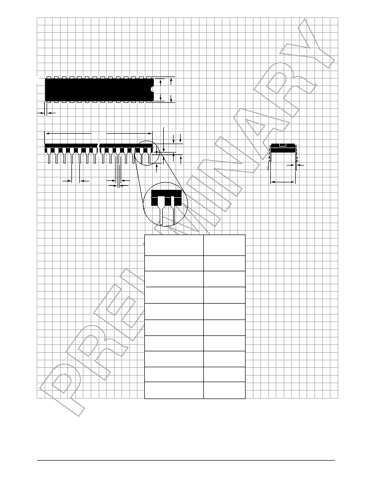
D
ALTERNATE
END PINS
(BOTH ENDS)
D1 = 0.005" min.
(0.127 min.)
E
PACKAGE: PLASTIC
DUAL≠IN≠LINE
(NARROW)
DIMENSIONS (Inches)
Minimum/Maximum
(mm)
A = 0.210" max.
(5.334 max).
E1
C
ÿ
L
A2
A1 = 0.015" min.
(0.381min.)
B
B1
e = 0.100 BSC
(2.540 BSC)
e
A
= 0.300 BSC
(7.620 BSC)
A2
B
B1
C
D
E
E1
L
ÿ
16≠PIN
0.115/0.195
(2.921/4.953)
0.014/0.022
(0.356/0.559)
0.045/0.070
(1.143/1.778)
0.008/0.014
(0.203/0.356)
0.780/0.800
(19.812/20.320)
0.300/0.325
(7.620/8.255)
0.240/0.280
(6.096/7.112)
0.115/0.150
(2.921/3.810)
0∞/ 15∞
(0∞/15∞)

13
SP432DS/10 SP432 High Speed, Low Power Quad Differential Line Receiver © Copyright 1997 Sipex Corporation
D
E
H
PACKAGE: PLASTIC
SMALL OUTLINE (SOIC)
(NARROW)
DIMENSIONS (Inches)
Minimum/Maximum
(mm)
A
A1
ÿ
L
B
e
h x 45∞
A
A1
B
D
E
e
H
h
L
ÿ
16≠PIN
0.053/0.069
(1.346/1.748)
0.004/0.010
(0.102/0.249)
0.013/0.020
(0.330/0.508)
0.386/0.394
(9.802/10.000)
0.150/0.157
(3.802/3.988)
0.050 BSC
(1.270 BSC)
0.228/0.244
(5.801/6.198)
0.010/0.020
(0.254/0.498)
0.016/0.050
(0.406/1.270)
0∞/8∞
(0∞/8∞)

14
SP432DS/10 SP432 High Speed, Low Power Quad Differential Line Receiver © Copyright 1997 Sipex Corporation
ORDERING INFORMATION
Model .................................................................................... Temperature Range ..................................................................................... Package
SP432CP ..................................................................................... 0
∞
C to +70
∞
C ....................................................................................... 16≠pin DIP
SP432CN ..................................................................................... 0
∞
C to +70
∞
C .................................................................................... 16≠pin SOIC
Corporation
SIGNAL PROCESSING EXCELLENCE
Sipex Corporation reserves the right to make changes to any products described herein. Sipex does not assume any liability arising out of the
application or use of any product or circuit described hereing; neither does it convey any license under its patent rights nor the rights of others.
Sipex Corporation
Headquarters and
Sales Office
22 Linnell Circle
Billerica, MA 01821
TEL: (978) 667-8700
FAX: (978) 670-9001
e-mail: sales@sipex.com
Sales Office
233 South Hillview Drive
Milpitas, CA 95035
TEL: (408) 934-7500
FAX: (408) 935-7600
Far East:
JAPAN:
Nippon Sipex Corporation
Yahagi No. 2 Building
3-5-3 Uchikanda, Chiyoda-ku
Tokyo 101
TEL: 81.3.3256.0577
FAX: 81.3.3256.0621
European Sales Offices:
ENGLAND:
Sipex Corporation
2 Linden House
Turk Street
Alton Hampshire GU34 IAN
England
TEL: 44-1420-549527
FAX: 44-1420-542700
e-mail: mikeb@sipex.co.uk
GERMANY:
Sipex GmbH
Gautinger Strasse 10
82319 Starnberg
TEL: 49.81.51.89810
FAX: 49.81.51.29598
e-mail: sipex-starnberg@t-online.de
Please consult the factory for pricing and availability on a Tape-On-Reel option.