 | –≠–ª–µ–∫—Ç—Ä–æ–Ω–Ω—ã–π –∫–æ–º–ø–æ–Ω–µ–Ω—Ç: SP489CS | –°–∫–∞—á–∞—Ç—å:  PDF PDF  ZIP ZIP |
1
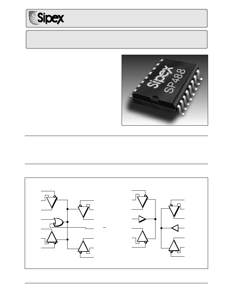
SP488/489
Quad RS-485/RS-422 Line Receivers
© Copyright 2000 Sipex Corporation
s
RS-485 or RS-422 Applications
s
Quad Differential Line Receivers
s
Tri≠state Output Control
s
120ns Typical Receiver Propagation
Delays
s
≠7V to +12V Common Mode Input
Range
s
1mA Supply Current
s
Single +5V Supply Operation
s
Pin Compatible with SN75173,
SN75175, LTC488 and LTC489
DESCRIPTION...
The SP488 and SP489 are low≠power quad differential line receivers meeting RS-485 and RS-422
standards. The SP488 features a common receiver enable control; the SP489 provides independent
receiver enable controls for each pair of receivers. Both feature tri≠state outputs and wide common≠
mode input range. The receivers have a fail≠safe feature which forces a logic "1" output when receiver
inputs are left floating. Both are available in 16≠pin plastic DIP and SOIC packages.
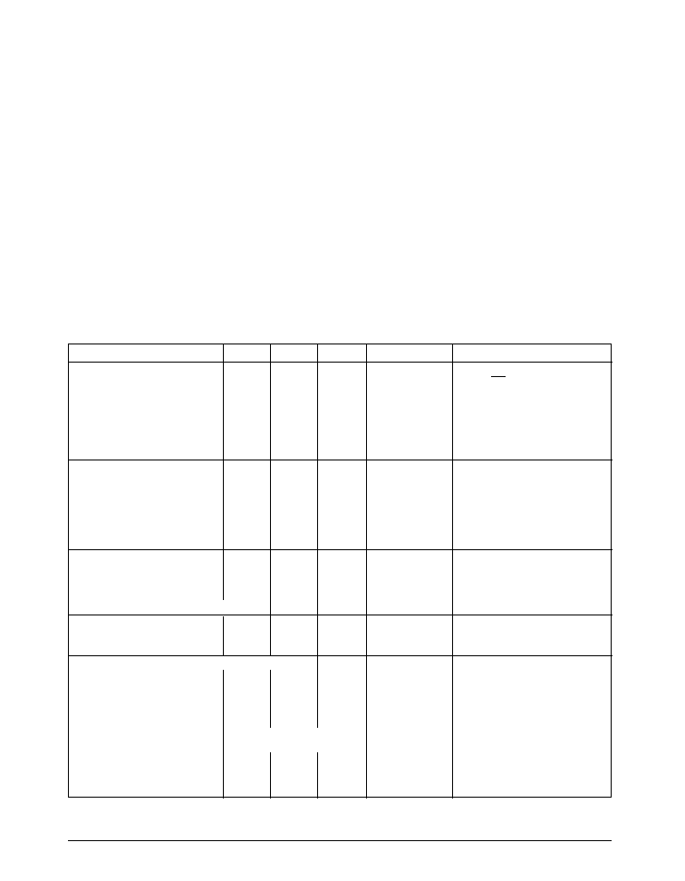
SP488
RI
1
B
RI
1
A
RO
1
EN
RO
2
RI
2
A
RI
2
B
GND
V
CC
RI
4
B
RI
4
A
RO
4
EN
RO
3
RI
3
A
RI
3
B
1
2
3
4
5
6
7
8
16
15
14
13
12
11
10
9
1
4
3
2
SP489
RI
1
B
RI
1
A
RO
1
EN
1
/EN
2
RO
2
RI
2
A
RI
2
B
GND
V
CC
RI
4
B
RI
4
A
RO
4
EN
3
/EN
4
RO
3
RI
3
A
RI
3
B
1
2
3
4
5
6
7
8
16
15
14
13
12
11
10
9
1
4
3
2
SP488/489
Quad RS-485/RS-422 Line Receivers
Æ
SP488/489
Quad RS-485/RS-422 Line Receivers
© Copyright 2000 Sipex Corporation
2
ABSOLUTE MAXIMUM RATINGS
These are stress ratings only and functional operation of the device
at these or any other above those indicated in the operation
sections of the specifications below is not implied. Exposure to
absolute maximum rating conditions for extended periods of time
may affect reliability.
V
CC
............................................................................................ +7V
Input Voltages
Logic ............................................................. ≠0.5V to (V
CC
+0.5V)
Receiver ...............................................................................
±
14V
Receiver Output Voltage ................................. ≠0.5V to (V
CC
+0.5V)
Input Currents
Logic ..................................................................................
±
25mA
Storage Temperature ............................................ ≠65
∞
C to +150
∞
C
Power Dissipation
Plastic DIP ........................................................................ 375mW
(derate 7mW/
∞
C above +70
∞
C)
Small Outline .................................................................... 375mW
(derate 7mW/
∞
C above +70
∞
C)
Lead Temperature (soldering, 10 sec) ................................... 300
∞
C
SPECIFICATIONS
V
CC
= 5V
±
5%; typicals at 25
∞
C; T
MIN
T
A
T
MAX
unless otherwise noted.
PARAMETER
MIN.
TYP.
MAX.
UNIT
CONDITIONS
DC CHARACTERISTICS
Digital Inputs
EN, EN, EN
1
/EN
2
, EN
3
/EN
4
Voltage
V
IL
0.8
Volts
V
IH
2.0
Volts
Input Current
±
2
µ
A
0V
V
IN
V
CC
RECEIVER INPUTS
Input Resistance
12
kOhm
≠7V
V
CM
12V
Differential Input Threshold
≠0.2
+0.2
Volts
≠7V
V
CM
12V
Input Current (A, B)
V
CC
= 0V or 5.25V; I
IN2
+1.0
mA
V
IN
= +12V
≠0.8
mA
V
IN
= ≠7V
Maximum Data Rate
10
Mbps
RECEIVER OUTPUTS
Output Voltage
V
OH
3.5
V
I
O
= ≠4mA; V
ID
= +0.2V
V
OL
0.4
V
I
O
= +4mA; V
ID
= ≠0.2V
High Impedance Output Current
±
1
µ
A
V
CC
= maximum; 0.4V
V
O
2.4V
POWER REQUIREMENTS
Supply Voltage
4.75
5.00
5.25
Volts
Supply Current
1
5
mA
No load
ENVIRONMENTAL AND MECHANICAL
Operating Temperature
≠C
0
+70
∞
C
≠E
≠40
+85
∞
C
Storage Temperature
≠65
+150
∞
C
Package
≠_S
16≠pin Plastic DIP
≠_T
16≠pin SOIC

3
SP488/489
Quad RS-485/RS-422 Line Receivers
© Copyright 2000 Sipex Corporation
A
B
54
100pF
DI
1/4 SP486
1/4 SP488
100pF EN
EN
ROn
DRIVER
RCVR
C
L
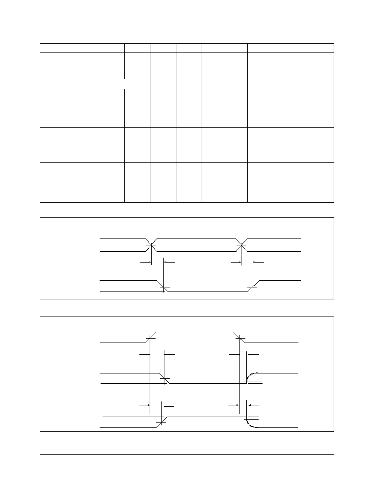
Figure 1. Timing Test Circuit
S
1
RCVR
S
2
V
CC
1k
C
L
1k
Figure 2. Enable/Disable Timing Test Circuit
Pin 6 -- RI
2
A -- Receiver 2 input A.
Pin 7 -- RI
2
B -- Receiver 2 input B.
Pin 8 -- GND -- Digital Ground.
Pin 9 -- RI
3
B -- Receiver 3 input B.
Pin 10 -- RI
3
A
--
Receiver 3 input A.
Pin 11 -- RO
3
-- Receiver 3 Output -- If
Receiver 3 output is enabled, if RI
3
A > RI
3
B by
200mV, Receiver 3 output is high. If Receiver 3
output is enabled, and if RI
3
A < RI
3
B by
200mV, Receiver 3 output is low.
Pin 12 -- EN -- Receiver Output Enable. Please
refer to SP488 Truth Table (1).
SP488 PINOUT
Pin 1 -- RI
1
B -- Receiver 1 input B.
Pin 2 -- RI
1
A
--
Receiver 1 input A.
Pin 3 -- RO
1
-- Receiver 1 Output -- If Re-
ceiver 1 output is enabled, if RI
1
A
> RI
1
B by
200mV, Receiver output is high. If Receiver 1
output is enabled, and if RI
1
A
< RI
1
B
by 200mV,
Receiver 1 output is low.
Pin 4 -- EN -- Receiver Output Enable. Please
refer to SP488 Truth Table (1).
Pin 5 -- RO
2
-- Receiver 2 Output -- If Re-
ceiver 2 output is enabled, if RI
2
A > RI
2
B by
200mV, Receiver 2 output is high. If Receiver 2
output is enabled, and if RI
2
A < RI
2
B by
200mV, Receiver 2 output is low.
SP488
RI
1
B
RI
1
A
RO
1
EN
RO
2
RI
2
A
RI
2
B
GND
V
CC
RI
4
B
RI
4
A
RO
4
EN
RO
3
RI
3
A
RI
3
B
1
2
3
4
5
6
7
8
16
15
14
13
12
11
10
9
1
4
3
2
SP489
RI
1
B
RI
1
A
RO
1
EN
1
/EN
2
RO
2
RI
2
A
RI
2
B
GND
V
CC
RI
4
B
RI
4
A
RO
4
EN
3
/EN
4
RO
3
RI
3
A
RI
3
B
1
2
3
4
5
6
7
8
16
15
14
13
12
11
10
9
1
4
3
2
PINOUT

SP488/489
Quad RS-485/RS-422 Line Receivers
© Copyright 2000 Sipex Corporation
4
Pin 13 -- RO
4
-- Receiver 4 Output -- If
Receiver 4 output is enabled, if RI
4
A > RI
4
B by
200mV, Receiver 4 output is high. If Receiver 4
output is enabled, and if RI
4
A < RI
4
B by
200mV, Receiver 4 output is low.
Pin 14 -- RI
4
A
-- Receiver 4 input A.
Pin 15 -- RI
4
B -- Receiver 4 input B.
Pin 16 -- Supply Voltage V
CC
-- 4.75V
V
CC
5.25V.
SP489 PINOUT
Pin 1 -- RI
1
B -- Receiver 1 input B.
Pin 2 -- RI
1
A --
Receiver 1 input A.
Pin 3 -- RO
1
--
Receiver 1 Output -- If Re-
ceiver 1 output is enabled, if RI
1A
> RI
1
B by
200mV, Receiver output is high. If Receiver 1
output is enabled, and if RI
1
A
< RI
1
B
by 200mV,
Receiver 1 output is low.
Pin 4 -- EN1/EN2 -- Receiver 1 and 2 Output
Enable. Please refer to SP489 Truth Table (2).
Pin 5 -- RO
2
-- Receiver 2 Output -- If Re-
ceiver 2 output is enabled, if RI
2
A > RI
2
B by
200mV, Receiver 2 output is high. If Receiver 2
output is enabled, and if RI
2
A < RI
2
B by
200mV, Receiver 2 output is low.
Pin 6 -- RI
2
A -- Receiver 2 input A.
Pin 7 -- RI
2
B -- Receiver 2 input B.
Pin 8 -- GND -- Digital Ground.
DIFFERENTIAL
ENABLES
OUTPUT
A ≠ B
EN
EN
RO
V
ID
0.2V
H
X
H
X
L
H
≠0.2V < V
ID
< +0.2V
H
X
X
X
L
X
V
ID
0.2V
H
X
L
X
L
L
X
L
H
Hi≠Z
Table 1. SP488 Truth Table
Pin 9 -- RI
3
B -- Receiver 3 input B.
Pin 10 -- RI
3
A --
Receiver 3 input A.
Pin 11 -- RO
3
-- Receiver 3 Output -- If
Receiver 3 output is enabled, if RI
3
A > RI
3
B by
200mV, Receiver 3 output is high. If Receiver 3
output is enabled, and if RI
3
A < RI
3
B by
200mV, Receiver 3 output is low.
Pin 12 -- EN3/EN4 -- Receiver 3 and 4 Output
Enable. Please refer to SP489 Truth Table (2).
Pin 13 -- RO
4
-- Receiver 4 Output -- If
Receiver 4 output is enabled, if RI
4
A > RI
4
B by
200mV, Receiver 4 output is high. If Receiver 4
output is enabled, and if RI
4
A < RI
4
B by
200mV, Receiver 4 output is low.
Pin 14 -- RI
4
A
-- Receiver 4 input A.
Pin 15 -- RI
4
B -- Receiver 4 input B.
Pin 16 -- Supply Voltage V
CC
-- 4.75V
V
CC
5.25V.
Table 2. SP489 Truth Table
DIFFERENTIAL
ENABLES
OUTPUT
A ≠ B
EN
1
/EN
2
or EN
3
/EN
4
RO
V
ID
0.2V
H
H
≠0.2V < V
ID
< +0.2V
H
X
V
ID
0.2V
H
L
X
L
Hi≠Z
FEATURES...
The SP488 and SP489 are low≠power quad
differential line receivers meeting RS-485 and
RS-422 standards. The SP488 features active
high and active low common receiver enable
controls; the SP489 provides independent, ac-
tive high receiver enable controls for each pair
of receivers. Both feature tri≠state outputs and a
-7V to +12V common≠mode input range per-
mitting a
±
7V ground difference between de-
vices on the communications bus. The SP488/
489 are equipped with a fail≠safe feature which
forces a logic high at the receiver output when
the input is left floating. Data rates up to 10Mbps
are supported. Both are available in 16-pin
plastic DIP and SOIC packages.
5
SP488/489
Quad RS-485/RS-422 Line Receivers
© Copyright 2000 Sipex Corporation
AC PARAMETERS
V
CC
= 5V
±
5%; typicals at 25
∞
C; 0
∞
C
T
A
+70
∞
C unless otherwise noted.
PARAMETER
MIN.
TYP.
MAX.
UNIT
CONDITIONS
PROPAGATION DELAY
Receiver Input to Output
C
L
= 15pF;
Figure 1, 3
Low to HIGH (tPLH)
120
250
ns
High to LOW (tPH
L
)
120
250
ns
Differential Receiver Skew (t
SKD
)
13
ns
Receiver Rise Time (t
R
)
10% to 90%
SP488
30
70
ns
SP489
30
70
ns
Receiver Fall Time (t
F
)
90% to 10%
SP488
20
40
ns
SP489
20
40
ns
RECEIVER ENABLE
To Output HIGH
70
150
ns
C
L
= 15pF;
Figures 2 and 4
(S2 closed)
To Output LOW
80
200
ns
CL = 15pF;
Figures 2 and 4
(S1 closed)
RECEIVER DISABLE
From Output LOW
70
150
ns
CL = 15pF;
Figures 2 and 4
(S1 closed)
From Output HIGH
70
150
ns
CL = 15pF;
Figures 2 and 4
(S2 closed)
Figure 4. Receiver Enable/Disable Timing
3V
0V
5V
V
OH
0V
Output normally low
F = 1MHZ: t
r
< 10ns: t
f
< 10ns
t
ZL
t
LZ
EN
V
OL
1.5V
1.5V
1.5V
0.5V
1.5V
0.5V
Output normally high
RO
t
ZH
RO
t
HZ
Figure 3. Receiver Propagation Delays
F = 1MHZ: t
r
< 10ns: t
f
< 10ns
t
PHL
t
PLH
V
OL
0V
0V
1.5V
RO
V
OH
1.5V
≠V
OD
+V
OD
Input A≠B