1
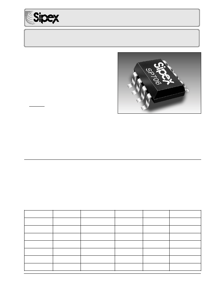
Rev. 10-17-00 SP706 +3.0/ +3.3 Low Power Microprocessor Circuits © Copyright 2000 Sipex Corporation
SP706P/R/S/T, SP708R/S/T
s
Precision Low Voltage Monitor:
SP706P/R and SP708R at +2.63V
SP706S and SP708S at +2.93V
SP706T and SP708T at +3.08V
s
RESET Pulse Width - 200ms
s
Independent Watchdog Timer - 1.6 sec
Timeout (SP706P/S/R/T)
s
40
µ
A Maximum Supply Current
s
Debounced TTL/CMOS Manual-Reset Input
s
RESET Asserted Down to V
CC
= 1V
s
RESET Output:
SP706P Active-High
SP706R/S/T Active-Low
SP708R/S/T Both Active High + Active Low
s
WDI Can Be Left Floating, Disabling the
Watchdog Function
DESCRIPTION
The SP706P/S/R/T, SP708R/S/T series is a family of microprocessor (
µ
P) supervisory circuits
that integrate myriad components involved in discrete solutions which monitor power-supply and
battery, in
µ
P, and digital systems. The SP706P/S/R/T, SP708R/S/T series will significantly
improve system reliability and operational efficiency when compared to results obtained with
discrete components. The features of the SP706P/S/R/T, SP708R/S/T series include a
watchdog timer, a
µ
P reset, a Power Fail Comparator, and a manual-reset input. The SP706P/
S/R/T, SP708R/S/T series is ideal for +3.0V or +3.3V applications in automotive systems,
computers, controllers, and intelligent instruments. The SP706P/S/R/T, SP708R/S/T series is
an ideal solution for systems in which critical monitoring of the power supply to the
µ
P and related
digital components is demanded.
r
e
b
m
u
N
t
r
a
P
e
v
i
t
c
A
T
E
S
E
R
d
l
o
h
s
e
r
h
T
T
E
S
E
R
t
e
s
e
R
l
a
u
n
a
M
y
c
a
r
u
c
c
A
I
F
P
t
u
p
n
I
g
o
d
h
c
t
a
W
P
6
0
7
P
S
H
G
I
H
V
3
6
.
2
S
E
Y
%
4
S
E
Y
R
6
0
7
P
S
W
O
L
V
3
6
.
2
S
E
Y
%
4
S
E
Y
S
6
0
7
P
S
W
O
L
V
3
9
.
2
S
E
Y
%
4
S
E
Y
T
6
0
7
P
S
W
O
L
V
8
0
.
3
S
E
Y
%
4
S
E
Y
R
8
0
7
P
S
H
G
I
H
/
W
O
L
V
3
6
.
2
S
E
Y
%
4
O
N
S
8
0
7
P
S
H
G
I
H
/
W
O
L
V
3
9
.
2
S
E
Y
%
4
O
N
T
8
0
7
P
S
H
G
I
H
/
W
O
L
V
8
0
.
3
S
E
Y
%
4
O
N
s
Built-In V
cc
Glitch Immunity
s
Available in 8-pin PDIP, NSOIC, and
µ
SOIC packages
s
Voltage Monitor for Power Failure or Low
Battery Warning
s
Pin Compatible Enhancement to Industry
Standards 706P/R/S/T and 708R/S/T
+3.0V/+3.3V Low Power Microprocessor
Supervisory Circuits
Æ
2
Rev. 10-17-00 SP706 +3.0/ +3.3 Low Power Microprocessor Circuits © Copyright 2000 Sipex Corporation
SPECIFICATIONS
V
cc
= 2.7V to 5.5V for SP70_P/R, V
CC
= 3.0 to 5.5V for SP70_S, V
CC
= 3.15V to 5.5V for SP70_T, T
A
= T
MIN
to T
MAX
to T
MAX
, unless otherwise noted,
typical at 25
∞
C.
ABSOLUTE MAXIMUM RATINGS
These are stress ratings only and functional operation
of the device at these ratings or any other above those
indicated in the operation sections of the specifications
below is not implied. Exposure to absolute maximum
rating conditions for extended periods of time may
affect reliability.
Terminal Voltage (with respect to GND):
V
CC
........................................................-0.3V to +6.0V
All Other Inputs (Note 1)..............-0.3V to (V
CC
+3.0V)
Input Current:
V
CC
.....................................................................20mA
GND...................................................................20mA
Output Current (all outputs)...............................20mA
ESD Rating...........................................................2kV
R
E
T
E
M
A
R
A
P
.
N
I
M
.
P
Y
T
.
X
A
M
S
T
I
N
U
S
N
O
I
T
I
D
N
O
C
V
,
e
g
n
a
R
e
g
a
t
l
o
V
g
n
i
t
a
r
e
p
O
C
C
0
.
1
5
.
5
V
I
,
t
n
e
r
r
u
C
y
l
p
p
u
S
Y
L
P
P
U
S
5
2
0
4
µ
A
V
=
R
M
C
C
g
n
i
t
a
o
l
F
I
D
W
,
g
n
i
t
a
o
l
F
r
o
d
l
o
h
s
e
r
h
T
t
e
s
e
R
5
5
.
2
5
8
.
2
0
0
.
3
3
6
.
2
3
9
.
2
8
0
.
3
0
7
.
2
0
0
.
3
5
1
.
3
V
R
/
P
_
0
7
P
S
S
_
0
7
P
S
T
_
0
7
P
S
s
i
s
e
r
e
t
s
y
H
d
l
o
h
s
e
r
h
T
t
e
s
e
R
0
2
V
m
2
e
t
o
N
t
,
h
t
d
i
W
e
s
l
u
P
t
e
s
e
R
S
R
0
4
1
0
0
2
0
8
2
s
m
2
e
t
o
N
T
E
S
E
R
e
g
a
t
l
o
V
t
u
p
t
u
O
V
H
O
V
L
O
V
H
O
V
L
O
V
x
8
.
0
C
C
V
C
C
5
.
1
-
3
.
0
4
.
0
V
V
)
X
A
M
(
T
S
R
V
<
C
C
I
,
V
6
.
3
<
E
C
R
U
O
S
0
0
5
=
µ
A
V
)
X
A
M
(
T
S
R
V
<
C
C
I
,
V
6
.
3
<
K
N
I
S
2
.
1
=
mA
V
<
V
5
.
4
C
C
I
,
V
5
.
5
<
E
C
R
U
O
S
0
0
8
=
µ
A
V
<
V
5
.
4
C
C
I
,
V
5
.
5
<
K
N
I
S
A
m
2
.
3
=
e
g
a
t
l
o
V
t
u
p
t
u
O
T
E
S
E
R
V
H
O
V
L
O
V
H
O
V
L
O
V
C
C
6
.
0
-
V
C
C
5
.
1
-
3
.
0
4
.
0
V
V
)
X
A
M
(
T
S
R
V
<
C
C
I
,
V
6
.
3
<
E
C
R
U
O
S
5
1
2
=
µ
A
V
)
X
A
M
(
T
S
R
V
<
C
C
I
,
V
6
.
3
<
E
C
R
U
O
S
A
m
2
.
1
=
V
<
V
5
.
4
C
C
I
,
V
5
.
5
<
E
C
R
U
O
S
0
0
8
=
µ
A
V
<
V
5
.
4
C
C
I
,
V
5
.
5
<
E
C
R
U
O
S
A
m
2
.
3
=
t
,
d
o
i
r
e
P
t
u
o
e
m
i
T
g
o
d
h
c
t
a
W
D
W
0
0
.
1
0
6
.
1
5
2
.
2
s
V
C
C
V
6
.
3
<
t
,
h
t
d
i
W
e
s
l
u
P
I
D
W
P
W
0
5
s
n
V
L
I
V
,
V
4
.
0
=
H
I
V
x
8
.
0
=
C
C
,
d
l
o
h
s
e
r
h
T
t
u
p
n
I
I
D
W
V
L
I
V
H
I
V
L
I
V
H
I
V
x
7
.
0
C
C
5
.
3
6
.
0
8
.
0
V
V
)
X
A
M
(
T
S
R
V
<
C
C
V
6
.
3
<
V
T
S
R
)
X
A
M
(
V
<
C
C
V
6
.
3
<
V
C
C
V
0
.
5
=
V
C
C
V
0
.
5
=
t
n
e
r
r
u
C
t
u
p
n
I
I
D
W
1
-
2
0
.
0
1
µ
A
V
r
o
0
=
I
D
W
C
C
Continuous Power Dissipation
Plastic DIP
(derate 9.09mW/
O
C above +70
O
C)..................727mW
SO
(derate 5.88mW/
O
C above +70
O
C)..................471mW
Mini SO
(derate 4.10mW/
O
C above +70
O
C)..................330mW
Storage Temperature Range.............-65∞C to +160∞C
Lead Temperature (solding 10 sec)................+300∞C

3
Rev. 10-17-00 SP706 +3.0/ +3.3 Low Power Microprocessor Circuits © Copyright 2000 Sipex Corporation
SPECIFICATIONS (continued)
V
cc
= 2.7V to 5.5V for SP70_P/R, V
CC
= 3.0 to 5.5V for SP70_S, V
CC
= 3.15V to 5.5V for SP70_T, T
A
= T
MIN
to T
MAX
to T
MAX
, unless otherwise noted,
typical at 25
∞
C.
R
E
T
E
M
A
R
A
P
.
N
I
M
.
P
Y
T
.
X
A
M
S
T
I
N
U
S
N
O
I
T
I
D
N
O
C
e
g
a
t
l
o
V
t
u
p
t
u
O
O
D
W
V
H
O
V
L
O
V
H
O
V
L
O
V
x
8
.
0
C
C
V
C
C
5
.
1
-
3
.
0
4
.
0
V
V
)
X
A
M
(
T
S
R
V
<
C
C
I
,
V
6
.
3
<
E
C
R
U
O
S
0
0
5
=
µ
A
V
)
X
A
M
(
T
S
R
V
<
C
C
I
,
V
6
.
3
<
K
N
I
S
A
m
2
.
1
=
V
<
V
5
.
4
C
C
I
,
V
5
.
5
<
E
C
R
U
O
S
0
0
8
=
µ
A
V
<
V
5
.
4
C
C
I
,
V
5
.
5
<
K
N
I
S
A
m
2
.
3
=
R
M
t
n
e
r
r
u
C
p
U
-
ll
u
P
5
2
0
0
1
0
7
0
5
2
0
5
2
0
0
6
µ
A
R
M
V
,
V
0
=
)
X
A
M
(
T
S
R
V
<
C
C
V
6
.
3
<
V
<
V
5
.
4
,
V
0
=
R
M
C
C
V
5
.
5
<
R
M
t
,
h
t
d
i
W
e
s
l
u
P
R
M
0
0
5
0
5
1
s
n
V
)
X
A
M
(
T
S
R
V
<
C
C
V
6
.
3
<
V
<
V
5
.
4
C
C
V
5
.
5
<
R
M
d
l
o
h
s
e
r
h
T
t
u
p
n
I
V
L
I
V
H
I
V
L
I
V
H
I
V
x
7
.
0
C
C
0
.
2
6
.
0
8
.
0
V
V
)
X
A
M
(
T
S
R
V
<
C
C
V
6
.
3
<
V
)
X
A
M
(
T
S
R
V
<
C
C
V
6
.
3
<
V
<
V
5
.
4
C
C
V
5
.
5
<
V
<
V
5
.
4
C
C
V
5
.
5
<
R
M
t
,
y
a
l
e
D
t
u
O
t
e
s
e
R
o
t
D
M
0
5
7
0
5
2
s
n
V
)
X
A
M
(
T
S
R
V
<
C
C
2
E
T
O
N
,
V
6
.
3
<
V
<
V
5
.
4
C
C
2
E
T
O
N
,
V
5
.
5
<
d
l
o
h
s
e
r
h
T
t
u
p
n
I
I
F
P
0
2
.
1
5
2
.
1
0
3
.
1
V
V
C
C
e
h
t
r
o
f
V
0
.
3
=
R
/
P
_
0
7
P
S
V
,
C
C
=
e
h
t
r
o
f
V
3
.
3
T
/
S
_
0
7
P
S
g
n
il
l
a
f
I
F
P
,
t
n
e
r
r
u
C
t
u
p
n
I
I
F
P
0
0
.
5
2
-
1
0
.
0
0
0
.
5
2
A
n
O
F
P
e
g
a
t
l
o
V
t
u
p
t
u
O
V
H
O
V
L
O
V
H
O
V
L
O
V
x
8
.
0
C
C
V
C
C
5
.
1
-
3
.
0
4
.
0
V
V
)
X
A
M
(
T
S
R
V
<
C
C
I
,
V
6
.
3
<
E
C
R
U
O
S
0
0
5
=
µ
A
V
)
X
A
M
(
T
S
R
V
<
C
C
I
,
V
6
.
3
<
K
N
I
S
2
.
1
=
mA
V
<
V
5
.
4
C
C
I
,
V
5
.
5
<
E
C
R
U
O
S
0
0
8
=
µ
A
V
<
V
5
.
4
C
C
I
,
V
5
.
5
<
K
N
I
S
A
m
2
.
3
=

