 | –≠–ª–µ–∫—Ç—Ä–æ–Ω–Ω—ã–π –∫–æ–º–ø–æ–Ω–µ–Ω—Ç: SP708 | –°–∫–∞—á–∞—Ç—å:  PDF PDF  ZIP ZIP |

1
SP705DS/09
SP705 Low Power Microprocessor Supervisory Circuits
© Copyright 2000 Sipex Corporation
SP705-708/813L/813M
Low Power Microprocessor Supervisory Circuits
s
Precision Voltage Monitor:
SP705/707/813L at 4.65V
SP706/708/813M at 4.40V
s
RESET Pulse Width - 200ms
s
Independent Watchdog Timer - 1.6s
Timeout (SP705/706/813L/813M)
s
60
µ
A Maximum Supply Current
s
Debounced TTL/CMOS Manual Reset Input
s
RESET Asserted Down to V
CC
= 1V
s
Voltage Monitor for Power Failure or Low
Battery Warning
s
Available in 8-pin PDIP, NSOIC, and
µ
SOIC packages
s
Pin Compatible Enhancement to Industry Standard 705-708/813L Series
s
Functionally Compatible to Industry Standard 1232 Series
DESCRIPTION...
The SP705-708/813L/813M series is a family of microprocessor (
µ
P) supervisory circuits that
integrate myriad components involved in discrete solutions which monitor power-supply and
battery in
µ
P and digital systems. The SP705-708/813L/813M series will significantly improve
system reliability and operational efficiency when compared to solutions obtained with discrete
components. The features of the SP705-708/813L/813M series include a watchdog timer,
a
µ
P reset, a Power Fail Comparator, and a manual-reset input. The SP705-708/813L/813M
series is ideal for applications in automotive systems, computers, controllers, and intelligent
instruments. The SP705-708/813L/813M series is an ideal solution for systems in which critical
monitoring of the power supply to the
µ
P and related digital components is demanded.
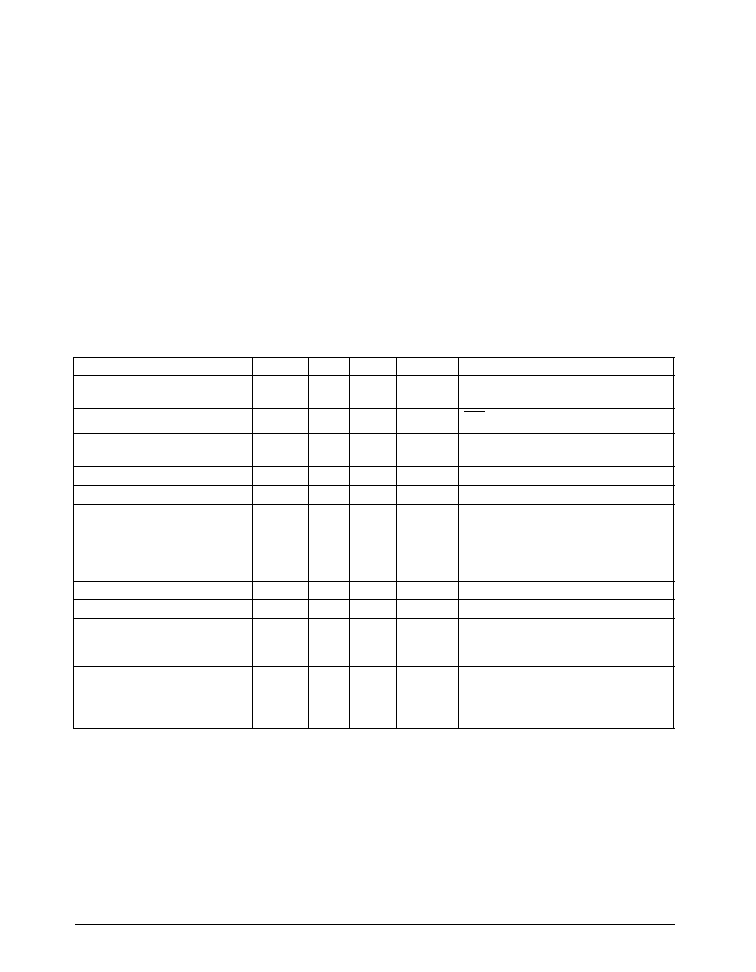
Part
RESET
RESET
Manual
PFI
Number
Threshold
Active
RESET
Watchdog
Accuracy
SP705
4.65 V
LOW
YES
YES
4%
SP706
4.40 V
LOW
YES
YES
4%
SP707
4.65 V
LOW and HIGH
YES
NO
4%
SP708
4.40 V
LOW and HIGH
YES
NO
4%
SP813L
4.65 V
HIGH
YES
YES
4%
SP813M
4.40V
HIGH
YES
YES
4%
Æ
SP705DS/09
SP705 Low Power Microprocessor Supervisory Circuits
© Copyright 2000 Sipex Corporation
2
R
E
T
E
M
A
R
A
P
.
N
I
M
.
P
Y
T
.
X
A
M
S
T
I
N
U
S
N
O
I
T
I
D
N
O
C
V
,
e
g
n
a
R
e
g
a
t
l
o
V
g
n
i
t
a
r
e
p
O
C
C
0
.
1
5
.
5
V
I
,
t
n
e
r
r
u
C
y
l
p
p
u
S
Y
L
P
P
U
S
0
4
0
6
µ
A
V
=
R
M
C
C
g
n
i
t
a
o
l
F
I
D
W
,
g
n
i
t
a
o
l
F
r
o
d
l
o
h
s
e
r
h
T
t
e
s
e
R
0
5
.
4
5
2
.
4
5
6
.
4
0
4
.
4
5
7
.
4
0
5
.
4
V
2
e
t
o
N
,
L
3
1
8
P
S
,
7
0
7
P
S
,
5
0
7
P
S
2
e
t
o
N
,
M
3
1
8
P
S
,
8
0
7
P
S
,
6
0
7
P
S
s
i
s
e
r
e
t
s
y
H
d
l
o
h
s
e
r
h
T
t
e
s
e
R
0
4
V
m
2
e
t
o
N
t
,
h
t
d
i
W
e
s
l
u
P
t
e
s
e
R
S
R
0
4
1
0
0
2
0
8
2
s
m
2
e
t
o
N
T
E
S
E
R
e
g
a
t
l
o
V
t
u
p
t
u
O
V
C
C
5
.
1
-
8
.
0
0
4
.
0
0
3
.
0
V
2
e
t
o
N
I
E
C
R
U
O
S
0
0
8
=
µ
A
I
E
C
R
U
O
S
4
=
µ
V
,
A
C
C
V
1
.
1
=
I
K
N
I
S
A
m
2
.
3
=
V
C
C
I
,
V
1
=
K
N
I
S
0
5
=
µ
A
t
,
d
o
i
r
e
P
t
u
o
e
m
i
T
g
o
d
h
c
t
a
W
D
W
0
0
.
1
0
6
.
1
5
2
.
2
s
M
3
1
8
P
S
,
L
3
1
8
P
S
,
6
0
7
P
S
,
5
0
7
P
S
t
,
h
t
d
i
W
e
s
l
u
P
I
D
W
P
W
0
5
s
n
V
L
I
V
,
V
4
.
0
=
H
I
V
X
8
.
0
=
C
C
,
d
l
o
h
s
e
r
h
T
t
u
p
n
I
I
D
W
W
O
L
H
G
I
H
5
.
3
8
.
0
V
M
3
1
8
P
S
,
L
3
1
8
P
S
,
6
0
7
P
S
,
5
0
7
P
S
V
C
C
V
5
=
t
n
e
r
r
u
C
t
u
p
n
I
I
D
W
5
7
-
0
3
0
2
-
5
7
µ
A
M
3
1
8
P
S
,
L
3
1
8
P
S
,
6
0
7
P
S
,
5
0
7
P
S
V
=
I
D
W
C
C
M
3
1
8
P
S
,
L
3
1
8
P
S
,
6
0
7
P
S
,
5
0
7
P
S
V
0
=
I
D
W
ABSOLUTE MAXIMUM RATINGS
This is a stress rating only and functional operation
of the device at these or any other conditions above
those indicated in the operation sections of this
specification is not implied. Exposure to absolute
maximum rating conditions for extended periods of
time may affect reliability and cause permanent
damage to the device.
V
cc
.......................................................................................
-0.3V to +6.0V
All Other Inputs (Note 1) ......... -0.3V to (Vcc+0.3V)
Input Current:
V
cc
.............................................................................................................
20mA
GND ............................................................ 20mA
Output Current (all outputs) ......................... 20mA
ESD Rating ..................................................... 4KV
Continuous Power Dissipation
Plastic DIP (derate 9.09mW/
∞
C above +70
∞
C)727mW
SO (derate 5.88mW/
∞
C above +70
∞
C) ...... 471mW
Mini SO (derate 4.10mW/
∞
C above +70
∞
C) 330mW
Storage Temperature Range ....... -65
∞
C to +160
∞
C
Lead Temperature (soldering, 10s) ............ +300
∞
C
SPECIFICATIONS
V
CC
= 4.75V to 5.50V for SP705/707/813L, V
CC
= 4.50V to 5.50V for SP706/708/813M, T
A
= T
MIN
to T
MAX
, unless otherwise noted, typical at 25
o
C.

3
SP705DS/09
SP705 Low Power Microprocessor Supervisory Circuits
© Copyright 2000 Sipex Corporation
R
E
T
E
M
A
R
A
P
.
N
I
M
.
P
Y
T
.
X
A
M
S
T
I
N
U
S
N
O
I
T
I
D
N
O
C
e
g
a
t
l
o
V
t
u
p
t
u
O
O
D
W
V
C
C
5
.
1
-
0
4
.
0
V
I
E
C
R
U
O
S
0
0
8
=
µ
A
I
K
N
I
S
A
m
2
.
3
=
R
M
t
n
e
r
r
u
C
p
U
-
ll
u
P
0
0
1
0
5
2
0
0
6
µ
A
R
M
V
0
=
R
M
t
,
h
t
d
i
W
e
s
l
u
P
R
M
0
5
1
s
n
R
M
d
l
o
h
s
e
r
h
T
t
u
p
n
I
W
O
L
H
G
I
H
0
.
2
8
.
0
V
R
M
t
,
y
a
l
e
D
t
u
O
t
e
s
e
R
o
t
D
M
0
5
2
s
n
2
e
t
o
N
d
l
o
h
s
e
r
h
T
t
u
p
n
I
I
F
P
0
2
.
1
5
2
.
1
0
3
.
1
V
V
C
C
V
5
=
t
n
e
r
r
u
C
t
u
p
n
I
I
F
P
0
0
.
5
2
-
1
0
.
0
0
0
.
5
2
A
n
O
F
P
e
g
a
t
l
o
V
t
u
p
t
u
O
V
C
C
5
.
1
-
4
.
0
V
I
E
C
R
U
O
S
0
0
8
=
µ
A
I
K
N
I
S
A
m
2
.
3
=
Note 1: The input voltage limits on PFI and MR can be exceeded if the input current is less than 10mA.
Note 2: Applies to both RESET in the SP705-SP708 and RESET in the SP707/708/813L/813M.
SPECIFICATIONS
V
CC
= 4.75V to 5.50V for SP705/707/813L,813M, V
CC
= 4.50V to 5.50V for SP706/708, T
A
= T
MIN
to T
MAX
, unless otherwise noted, typical at 25
o
C.
SP705
SP706
SP813L
SP813M
1
8
7
6
5
4
3
2
1
MR
V
CC
GND
PFI
WDO
RESET / RESET*
WDI
PFO
SP707
SP708
1
8
7
6
5
4
3
2
1
MR
V
CC
GND
PFI
RESET
RESET
N.C.
PFO
SP705
SP706
SP813L
SP813M
1
8
7
6
5
4
3
2
1
WDO
MR
V
CC
WDI
PFO
PFI
GND
SP707
SP708
1
8
7
6
5
4
3
2
1
RESET
RESET
MR
V
CC
N.C.
PFO
PFI
GND
RESET / RESET*
DIP and SOIC
µ
SOIC
Figure 1. Pinouts
* SP813L/M only
* SP813L/M only

SP705DS/09
SP705 Low Power Microprocessor Supervisory Circuits
© Copyright 2000 Sipex Corporation
4
E
M
A
N
N
O
I
T
C
N
U
F
N
O
I
T
P
I
R
C
S
E
D
N
I
P
6
0
7
/
5
0
7
P
S
8
0
7
/
7
0
7
P
S
M
3
1
8
/
L
3
1
8
P
S
/
P
I
D
C
I
O
S
C
I
O
S
C
I
O
S
C
I
O
S
C
I
O
S
C
I
O
S
µ
/
P
I
D
C
I
O
S
C
I
O
S
C
I
O
S
C
I
O
S
C
I
O
S
C
I
O
S
µ
/
P
I
D
C
I
O
S
C
I
O
S
C
I
O
S
C
I
O
S
C
I
O
S
C
I
O
S
µ
R
M
e
s
l
u
p
t
e
s
e
r
a
s
r
e
g
g
i
r
t
t
u
p
n
i
s
i
h
T
-
t
e
s
e
R
l
a
u
n
a
M
t
u
p
n
i
W
O
L
-
e
v
i
t
c
a
s
i
h
T
.
V
8
.
0
w
o
l
e
b
d
e
ll
u
p
n
e
h
w
0
5
2
l
a
n
r
e
t
n
i
n
a
s
a
h
µ
e
b
n
a
c
t
I
.
t
n
e
r
r
u
c
p
u
-
ll
u
p
A
d
e
t
r
o
h
s
r
o
e
n
il
c
i
g
o
l
S
O
M
C
r
o
L
T
T
a
m
o
r
f
n
e
v
i
r
d
h
c
t
i
w
s
a
h
t
i
w
d
n
u
o
r
g
o
t
1
3
1
3
1
3
V
C
C
y
l
p
p
u
s
r
e
w
o
p
V
5
+
2
4
2
4
2
4
D
N
G
s
l
a
n
g
i
s
ll
a
r
o
f
e
c
n
e
r
e
f
e
r
d
n
u
o
r
G
3
5
3
5
3
5
I
F
P
t
u
p
n
i
r
o
t
i
n
o
m
e
g
a
t
l
o
v
s
i
h
t
n
e
h
W
-
t
u
p
n
I
li
a
F
-
r
e
w
o
P
I
F
P
t
c
e
n
n
o
C
.
W
O
L
s
e
o
g
O
F
P
,
V
5
2
.
1
n
a
h
t
s
s
e
l
s
i
V
r
o
d
n
u
o
r
g
o
t
C
C
.
e
s
u
n
i
t
o
n
n
e
h
w
4
6
4
6
4
6
O
F
P
I
F
P
li
t
n
u
H
G
I
H
s
i
t
u
p
t
u
o
s
i
h
T
-
t
u
p
t
u
O
li
a
F
-
r
e
w
o
P
.
V
5
2
.
1
n
a
h
t
s
s
e
l
s
i
5
7
5
7
5
7
I
D
W
r
o
H
G
I
H
s
n
i
a
m
e
r
t
u
p
n
i
s
i
h
t
f
I
-
t
u
p
n
I
g
o
d
h
c
t
a
W
s
e
m
i
t
r
e
m
i
t
g
o
d
h
c
t
a
w
l
a
n
r
e
t
n
i
e
h
t
,
s
6
.
1
r
o
f
W
O
L
r
o
I
D
W
g
n
i
t
a
o
l
F
.
W
O
L
s
e
o
g
O
D
W
d
n
a
t
u
o
e
t
a
t
s
-
i
r
t
e
c
n
a
d
e
p
m
i
-
h
g
i
h
a
o
t
I
D
W
g
n
i
t
c
e
n
n
o
c
l
a
n
r
e
t
n
i
e
h
T
.
e
r
u
t
a
e
f
g
o
d
h
c
t
a
w
e
h
t
s
e
l
b
a
s
i
d
r
e
f
f
u
b
s
i
T
E
S
E
R
r
e
v
e
n
e
h
w
s
r
a
e
l
c
r
e
m
i
t
g
o
d
h
c
t
a
w
s
e
e
s
I
D
W
r
e
v
e
n
e
h
w
r
o
,
d
e
t
a
t
s
-
i
r
t
s
i
I
D
W
,
d
e
t
r
e
s
s
a
.
e
g
d
e
g
n
il
l
a
f
r
o
g
n
i
s
i
r
a
6
8
-
-
6
8
.
C
.
N
.
t
c
e
n
n
o
C
o
N
-
-
6
8
-
-
T
E
S
E
R
s
e
s
l
u
p
t
u
p
t
u
o
s
i
h
T
-
t
u
p
t
u
O
T
E
S
E
R
W
O
L
-
e
v
i
t
c
A
W
O
L
s
y
a
t
s
d
n
a
d
e
r
e
g
g
i
r
t
n
e
h
w
s
m
0
0
2
r
o
f
W
O
L
V
r
e
v
e
n
e
h
w
C
C
V
5
6
.
4
(
d
l
o
h
s
e
r
h
t
t
e
s
e
r
e
h
t
w
o
l
e
b
s
i
e
h
t
r
o
f
V
0
4
.
4
d
n
a
L
3
1
8
/
7
0
7
/
5
0
7
P
S
e
h
t
r
o
f
V
r
e
t
f
a
s
m
0
0
2
r
o
f
W
O
L
s
n
i
a
m
e
r
t
I
.
)
8
0
7
/
6
0
7
P
S
c
c
m
o
r
f
s
e
o
g
R
M
r
o
d
l
o
h
s
e
r
h
t
t
e
s
e
r
e
h
t
e
v
o
b
a
s
e
s
i
r
r
e
g
g
i
r
t
t
o
n
ll
i
w
t
u
o
e
m
i
t
g
o
d
h
c
t
a
w
A
.
H
G
I
H
o
t
W
O
L
.
R
M
o
t
d
e
t
c
e
n
n
o
c
s
i
O
D
W
s
s
e
l
n
u
T
E
S
E
R
7
1
7
1
-
-
O
D
W
n
e
h
w
W
O
L
s
ll
u
p
t
u
p
t
u
o
s
i
h
T
-
t
u
p
t
u
O
g
o
d
h
c
t
a
W
t
n
u
o
c
s
6
.
1
s
t
i
s
e
h
s
i
n
i
f
r
e
m
i
t
g
o
d
h
c
t
a
w
l
a
n
r
e
t
n
i
e
h
t
s
i
g
o
d
h
c
t
a
w
e
h
t
li
t
n
u
n
i
a
g
a
H
G
I
H
o
g
t
o
n
s
e
o
d
d
n
a
e
n
il
-
w
o
l
g
n
i
r
u
d
W
O
L
s
e
o
g
o
s
l
a
O
D
W
.
d
e
r
a
e
l
c
V
r
e
v
e
n
e
h
W
.
s
n
o
i
t
i
d
n
o
c
C
C
t
e
s
e
r
e
h
t
w
o
l
e
b
s
i
e
k
il
n
u
,
r
e
v
e
w
o
H
.
W
O
L
s
y
a
t
s
O
D
W
,
d
l
o
h
s
e
r
h
t
e
s
l
u
p
m
u
m
i
n
i
m
a
e
v
a
h
t
o
n
s
e
o
d
O
D
W
,
T
E
S
E
R
V
s
a
n
o
o
s
s
A
.
h
t
d
i
w
C
C
t
e
s
e
r
e
h
t
e
v
o
b
a
s
i
.
y
a
l
e
d
o
n
h
t
i
w
H
G
I
H
s
e
o
g
O
D
W
,
d
l
o
h
s
e
r
h
t
8
2
-
-
8
2
T
E
S
E
R
e
h
t
s
i
t
u
p
t
u
o
s
i
h
T
-
t
u
p
t
u
O
T
E
S
E
R
H
G
I
H
-
e
v
i
t
c
A
s
i
T
E
S
E
R
r
e
v
e
n
e
h
W
.
T
E
S
E
R
f
o
t
n
e
m
e
l
p
m
o
c
e
h
t
e
t
o
N
.
a
s
r
e
v
e
c
i
v
d
n
a
,
W
O
L
s
i
T
E
S
E
R
,
H
G
I
H
.
y
l
n
o
t
u
p
t
u
o
t
e
s
e
r
a
s
a
h
M
3
1
8
/
L
3
1
8
P
S
-
-
8
2
7
1
Table 1. Device Pin Description

5
SP705DS/09
SP705 Low Power Microprocessor Supervisory Circuits
© Copyright 2000 Sipex Corporation
1.25V
4.65V
(4.40V for the SP708)
V
CC
RESET
GENERATOR
250
µ
A
MR
V
CC
RESET
SP707
SP708
PFI
PFO
GND
RESET
Figure 3. Internal Block Diagram for the SP707/708
Figure 2. Internal Block Diagram for the SP705/706/813L/813M
SP705
SP706
SP813L
SP813M
GND
* For the SP813L/813M only
1.25V
4.65V
(4.40V for the SP706 and SP813M)
V
CC
TIMEBASE FOR
RESET AND
WATCHDOG
WATCHDOG
TIMER
RESET
GENERATOR
WATCHDOG
TRANSITION
DETECTOR
250
µ
A
MR
V
CC
RESET/RESET*
WDO
PFI
PFO
WDI