Äîêóìåíòàöèÿ è îïèñàíèÿ www.docs.chipfind.ru
1
Date: 6/20/06 Rev T SP7685, 1.2A Buck/BoostCharge Pump LED Driver © 2006 Sipex Corporation
SP7685
DESCRIPTION
The SP7685 is a current-regulated charge pump ideal for powering high brightness LEDs for
camera flash applications. The charge pump can be set to regulate two current levels for
FLASH and TORCH modes. The SP7685 automatically switches modes between step-up
and step-down ensuring that LED current does not depend on the forward voltage. A low
current sense reference voltage (50mV) allows the use of small 0603 current sensing
resistors. The SP7685 is offered in 10-pin DFN package.
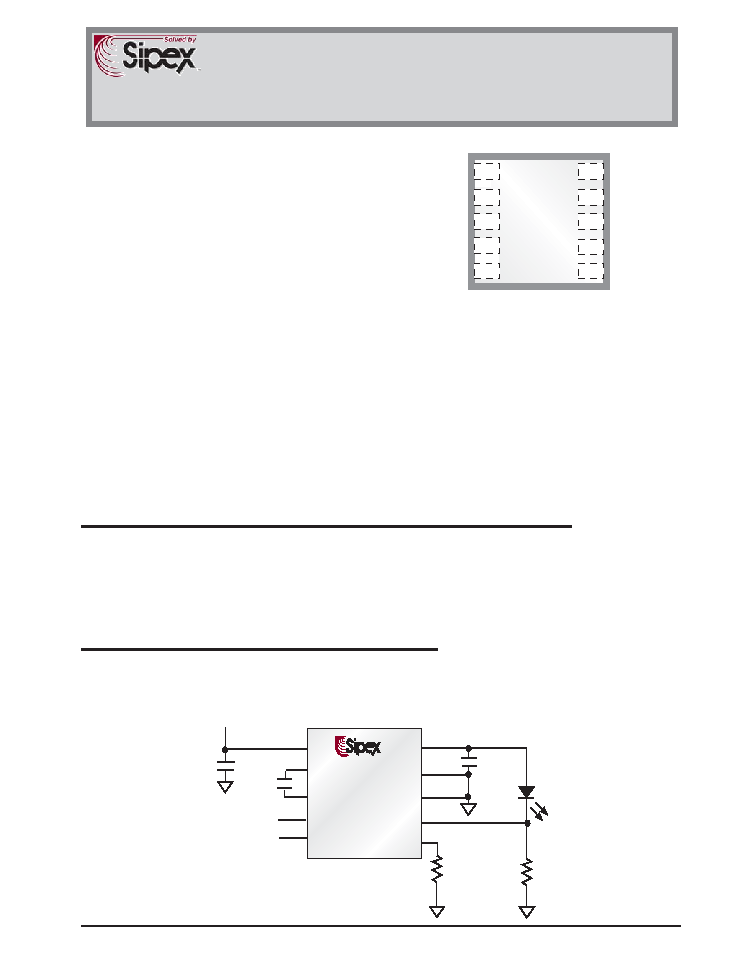
TYPICAL APPLICATION CIRCUIT
FEATURES
Output Current up to 1.2A
Up to 94% Efficiency in Torch Mode
Adjustable FLASH Mode Current
Minimum External Components: No Inductors
Automatic Buck/Boost Mode Switchover
Wide V
IN
Range: 2.7V to 5.5V
High Frequency Operation: 2.4 MHz
50mV Reference for low Loss Sensing
I
Q
< 2A in Shutdown
PWM Dimming Control
Automatic Soft Start Limits Inrush Current
Overvoltage Protection on Output
Overcurrent/temperature Protection
Low Ripple and EMI
Ultra-low Dropout Voltage in Buck Mode
2.6 Second Timeout in Flash Mode
Space Saving RoHS Compliant, Lead Free
Package: 10-pin 3mm x 3mm DFN
APPLICATIONS
White LED Torch/Flash for Cell
Phones, DSCs, and Camcorders
White LED Backlighting
Generic Lighting/Flash/Strobe
Applications
General Purpose High Current Boost
1.2A Buck/Boost Charge Pump LED Driver
SP7685
¤
ENABLE
TORCH/FLASH
C1
C2
FLASH
FB
P
GND
S
GND
R
SET
V
OUT
V
IN
10F
(3.0 - 4.2V)
10F
1F
EN
R
SENSE
R
SET
C
IN
C
OUT
C
FC
V
IN
1A Flash
200mA Torch
PWF1 WLED
80K
0.22
O
SP7685
10 Pin DFN
10
9
8
7
6
VOUT
PGND
SGND
FB
RSET
1
2
3
4
5
VIN
C1
C2
FLASH
EN
2
Date: 6/20/06 Rev T SP7685, 1.2A Buck/BoostCharge Pump LED Driver © 2006 Sipex Corporation
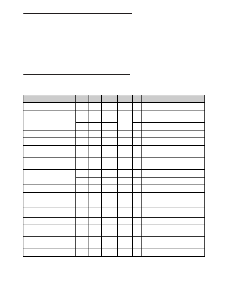
ELECTRICAL CHARACTERISTICS
T
A
= -40°C to +85°C, V
IN
=3.6V, C
IN
= 10F, C
FC
=1.0F, C
OUT
=10F. V
SHDN
= V
IN,
typical values at 25°C. The
denotes the specifications which apply over the full operating
temperature range unless otherwise noted.
V
IN
, V
OUT
.......................................................................
-0.3V to 6V
Output Current Pulse (Flash) ................................. 2A
Output Current Continuous (Torch) ..................... 0.4A
Storage Temperature ...................... -65°C to +150°C
Operating Temperature ..................... -40°C to +85°C
V
EN
............................................................ 0.0V to 7V
3x3 10 DFN .........................................O
JA
= 40.5°C/W
ESD Rating. ................................................ 2kV HBM
These are stress ratings only and functional operation of
the device at these ratings or any other above those
indicated in the operation sections of the specifications
below is not implied. Exposure to absolute maximum
rating conditions for extended periods of time may affect
reliability.
ABSOLUTE MAXIMUM RATINGS
PARAMETER
MIN.
TYP.
MAX.
UNITS
CONDITIONS
Operating Input Voltage
2.7
5.5
V
Quiescent Current
0.5
3
mA
V
IN
= 2.7 - 5.5V FLASH = GND,
1X Mode, I
LOAD
= 100A
2
FLASH = High, 2x mode
Shutdown Current
2
A
V
IN
= 5.5V, V
EN
= 0.0V
Oscillator Frequency
2.4
MHz
Charge Pump Equivalent
Resistance (x2 mode)
4
V
FB
= 0.0V, V
IN
= 3.6V
Charge Pump Equivalent
Resistance (x1 mode)
0.4
0.7
V
IN
= 3.6V
FB Reference Voltage
45
50
55
mV
FLASH = GND
138
150
162
mV
FLASH = High, R
SET
= 53.6k
.
FB Reference Voltage Range
100
400
mV
FLASH = High. Guaranteed by design.
FB Pin Current
0.5
A
V
FB
= 0.3V
EN, FLASH Logic Low
0.4
V
EN, FLASH Logic High
1.3
V
EN, FLASH Pin Current
0.5
A
V
OUT
Turn-on Time
170
500
s
V
IN
= 3.6V, FB within 90% of
regulation
Thermal Shutdown
Temperature
145
o
C
Maximum Flash ON time
1.6
2.6
3.6
s
FLASH = High

3
Date: 6/20/06 Rev T SP7685, 1.2A Buck/BoostCharge Pump LED Driver © 2006 Sipex Corporation
PIN DESCRIPTION
PIN
NUMBER
PIN NAME
DESCRIPTION
1
V
IN
Input Voltage for the charge pump. Decouple with
4.7µF ceramic capacitor close to the pins of the IC.
2
C1
Positive input for the external flying capacitor. Connect
a ceramic 1µF capacitor close to the pins of the IC.
3
C2
Negative input for the external flying capacitor. Connect
a ceramic 1µF capacitor close to the pins of the IC.
4
FLASH
Logic input to toggle operation between FLASH and
TORCH mode. In TORCH mode FB is regulated to the
internal 50mV reference. In FLASH mode FB reference
voltage can be adjusted by changing the resistor from
R
SET
pin to ground. Choose the external current sense
resistor (R
SENSE
) based on desired current in TORCH
mode. This pin does not have an internal pull-up/pull-
down; do not leave this pin floating.
5
EN
Shutdown control input. Connect to V
IN
for normal
operation, connect to ground for shutdown. This pin
does not have an internal pull-up/pull-down; do not
leave this pin floating.
6
R
SET
Connect a resistor from this pin to ground. When in
FLASH mode (FLASH = High) this resistor sets the
current regulation point according to the following: V
FB
=
R
SET
*14uA/5 (Flash Mode)
7
FB
Feedback input for the current control loop. Connect
directly to the current sense resistor.
8
S
GND
Internal ground pin. Control circuitry returns current to
this pin.
9
P
GND
Power ground pin.
Flying capacitor current returns
through this pin.
10
V
OUT
Charge Pump Output Voltage.
Decouple with an
external capacitor.
At least 1µF is recommended.
Higher capacitor values reduce output ripple
4
Date: 6/20/06 Rev T SP7685, 1.2A Buck/BoostCharge Pump LED Driver © 2006 Sipex Corporation
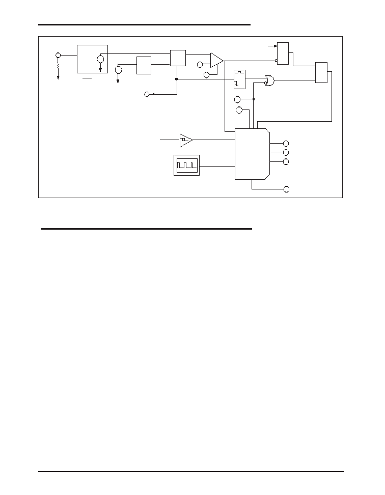
FUNCTIONAL DIAGRAM
The SP7685 is a charge pump regulator
designed for converting a Li-Ion battery
voltage of 2.7V to 4.2V to drive a white LED
used in digital still camera Flash and Torch
applications. The SP7685 has two modes
of operation which are pin-selectable for
either Flash or Torch. Flash mode is usually
used with a pulse of about 200 to 300
milliseconds to generate a high intensity
Flash. Torch can be used continuously at a
lower output current than Flash and is often
used for several seconds in a digital still
camera "movie" mode.
The SP7685 also has two modes of opera-
tion to control the output current: the 1X
mode and 2X mode. Operation begins after
the enable pin EN receives a logic high, the
bandgap reference wakes up after 200s,
and then SP7685 goes through a soft-start
mode designed to reduce inrush current.
The SP7685 starts in the 1X mode, which
THEORY OF OPERATION
acts like a linear regulator to control the
output current by continuously monitoring
the feedback pin FB. In 1X mode, if the
SP7685 auto detects a dropout condition,
which is when the FB pin is below the
regulation point for more than 32 cycles of
the internal clock, the SP7685 automati-
cally switches to the 2X mode. The SP7685
remains in the 2X mode until one of four
things happens: 1) the enable pin EN has
been toggled, 2) the Flash pin has changed
from high to low, 3) V
IN
is cycled or, 4) a
thermal fault occurs.
The 2X mode is the charge pump mode
where the output can be pumped as high as
two times the input voltage, provided the
output does not exceed the maximum volt-
age for the SP7685, which is internally
limited to about 5.5V. In the 2X mode, as in
the 1X mode, the output current is regulated
by the voltage at the FB pin.
RSET BLOCK
6
RSET
RSET
R
SET
REF=
{
5
R
SET
}
x 14A
+
-
1.26V
+
-
BG REF
RSET REF
RESISTOR
TAPS
50mV
4
FLASH
FLASH=1, S=1, RSET REF
FLASH=0, S=0, 50mV
1
0 s
MUX
2x1
FB REF
7
FB
SGND 8
FB
COM P
+
-
FB COMP
CLR
COUNTER
32 COUNT
ONE
SHOT
SET
DOMINANT
S
R
0
MODE SWITCH
0 =1X
1=2X
1
5
EN
VIN
135C ON
145C OFF
THERMAL FAULT
OVER TEMP COMP
CLK
CLK
2.4MH
Z
CHARGE
PUMP
SWITCHES
PGND
C1
C2
VOUT
CLK

5
Date: 6/20/06 Rev T SP7685, 1.2A Buck/BoostCharge Pump LED Driver © 2006 Sipex Corporation
In the Torch mode, (Flash = GND) the Flash
pin is set to logic low and the SP7685 FB pin
regulates to 50mV output:
V
FB
= 50mV (Torch Mode)
When in Flash mode, (Flash = V
IN
), the FB
regulation voltage is set by the resistor R
SET
connected between the R
SET
pin and S
GND
and the equation:
V
FB
= R
SET
* 14A / 5 (Flash Mode)
Where 14A is an internal regulated
current and 5 is an internal factor used to
scale the V
SET
voltage to the V
FB
voltage.
Typical values of R
SET
are 140K to
35K for a range of V
FB
= 400mV to
100mV in Flash mode.
The output current is then set in either Flash
or Torch mode by the equation:
I
OUT
= V
FB
/ R
SENSE
FLASH TIMEOUT PROTECTION
Due to the high currents typically available
in Flash mode, it is necessary to protect the
white LED from damage if left on too long.
The SP7685 has a timeout in Flash mode of
approximately 2.6 seconds after which it will
shut down operation. Operation will not
begin again in Flash mode until the Enable
pin or Flash pin have been set Low and then
High again.
OVERTEMPERATURE PROTECTION
When the temperature of the SP7685 rises
above 145
°
C, the overtemperature protec-
THEORY OF OPERATION
tion circuitry turns off the output switches
to prevent damage to the device. If the
temperature drops back down below 135
degrees Celsius, the part automatically
recovers and executes a soft start cycle.
OVERVOLTAGE PROTECTION
The SP7685 has over voltage protec-
tion. If the output voltage rises above
the 5.5V threshold, the over voltage
protection shuts off all of the output
switches to prevent the output voltage
from rising further. When the output
decreases below 5.5V, the device re-
sumes normal operation.
OVERCURRENT PROTECTION
The over current protection circuitry moni-
tors the average current out of the V
OUT
pin. If the average output current exceeds
approximately 1.6 Amps, then the
overcurrent protection circuitry shuts off
the output switches to protect the chip.
BRIGHTNESS CONTROL USING PWM
Dimming control can be achieved by ap-
plying a PWM control signal to the EN pin.
The brightness of the white LEDs is con-
trolled by increasing and decreasing the
duty cycle of the PWM signal. While the
operating frequency range of the PWM
control is from 60Hz to 700Hz, the recom-
mended maximum brightness frequency
range of the PWM signal is from 60Hz to
200Hz. A repetition rate of at least 60Hz is
required to prevent flicker.
6
Date: 6/20/06 Rev T SP7685, 1.2A Buck/BoostCharge Pump LED Driver © 2006 Sipex Corporation
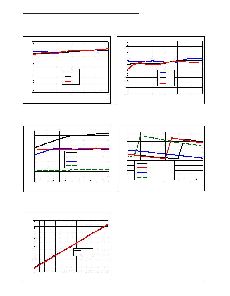
SP7685 VFB vs RSET
0
50
100
150
200
250
300
350
400
450
10
20
30
40
50
60
70
80
90 100 110 120 130 140 150
RSET (K)
VFB (mV)
Measured
Calculated
SP7685 Output Efficiency
0
10
20
30
40
50
60
70
80
90
100
3.0
3.2
3.4
3.6
3.8
4.0
4.2
Input Voltage (V)
Efficiency (%)
1000mA,Vf=3.31V PWF1
700mA,Vf=3.18V PWF1
700mA,Vf=3.92V AOT
200mA,Torch
SP7685 Output Current
0
100
200
300
400
500
600
700
800
900
1000
1100
3.0
3.2
3.4
3.6
3.8
4.0
4.2
Input Voltage (V)
Output Current (mA)
1000mA,Vf=3.31V PWF1
700mA,Vf=3.24V PWF1
700mA,Vf=3.92V AOT
200mA,Torch Mode
SP7685 Torch Output Current
0
50
100
150
200
250
300
3.0
3.2
3.4
3.6
3.8
4.0
4.2
Input Voltage (V)
Output Current (mA)
-40C
25C
85C
SP7685 700mA Flash output Current
400
450
500
550
600
650
700
750
800
850
900
3.0
3.2
3.4
3.6
3.8
4.0
4.2
Input Voltage (V)
Output Current (mA)
-40C
25C
85C
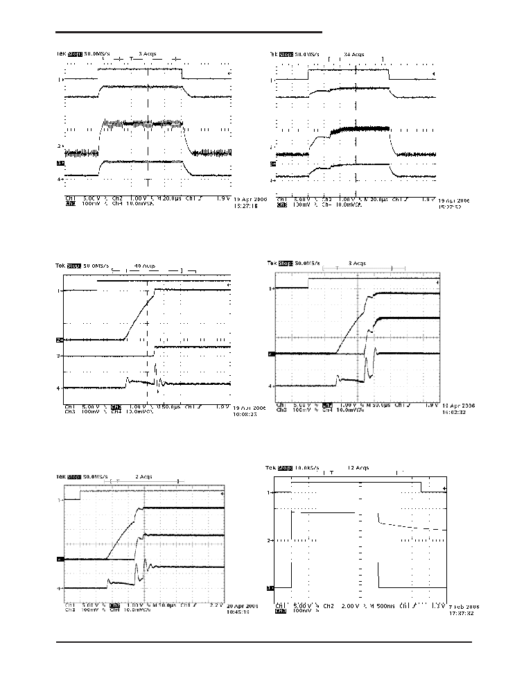
APPLICATION INFORMATION
V
IN
=3.6V, Typical Application Circuit, T
A
= 25°C unless otherwise noted.
7
Date: 6/20/06 Rev T SP7685, 1.2A Buck/BoostCharge Pump LED Driver © 2006 Sipex Corporation
APPLICATION INFORMATION
EN
V
OU
V
FB
I
IN
1A/div
Start Up 700mA Flash
V
IN
=3.6V, V
OUT
=3.6V
EN
V
OUT
V
FB
I
OUT
1A/div
Torch in 1X to Flash in 2X Mode, V
IN
=3.6V
EN
V
OUT
V
FB
I
IN
1A/div
Start Up 200mA Torch
V
IN
=3.6V, V
OUT
=3.1V
V
IN
=3.6V, Typical Application Circuit, T
A
= 25°C unless otherwise noted.
Flash Mode TimeOut Circuit at 2.6sec.
V
IN
=4.2V, I
OUT
=1A
V
FB
V
OUT
EN
EN
V
OU
V
FB
I
IN
1A/div
Start Up 1000mA Flash
V
IN
=3.6V, V
OUT
=3.8V
EN
V
OUT
V
FB
I
OUT
1A/div
Torch in 1X to Flash in 1X Mode, V
IN
=4.2V
8
Date: 6/20/06 Rev T SP7685, 1.2A Buck/BoostCharge Pump LED Driver © 2006 Sipex Corporation
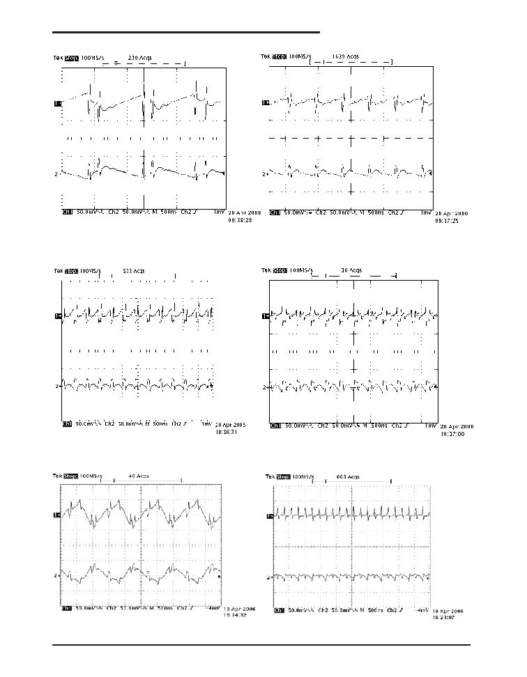
APPLICATION INFORMATION
Input
Ripple
Ripple 1X Torch 200mA, V
IN
=4.2V
Output
Ripple
Input
Ripple
Ripple 2X Torch 200mA, V
IN
=3.0V
Output
Ripple
Input
Ripple
Ripple 1X Flash 700mA, V
IN
=4.2V
Output
Ripple
Input
Ripple
Ripple 2X Flash 700mA, V
IN
=3.6V
Output
Ripple
V
IN
=3.6V, Typical Application Circuit, T
A
= 25°C unless otherwise noted.
Input
Ripple
Ripple 1X Flash 1000mA, V
IN
=4.2V
Output
Ripple
Input
Ripple
Ripple 2X Flash 1000mA, V
IN
=3.6V
Output
Ripple
9
Date: 6/20/06 Rev T SP7685, 1.2A Buck/BoostCharge Pump LED Driver © 2006 Sipex Corporation
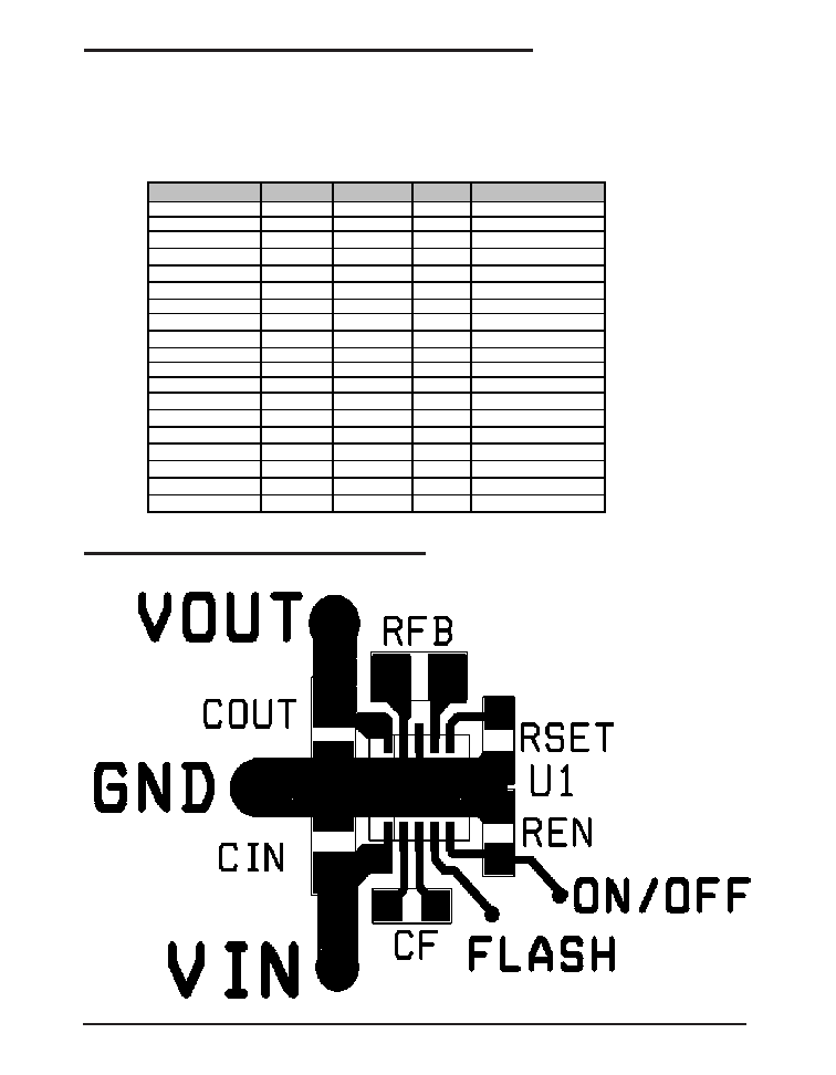
COMPONENT SELECTION
The input and output capacitors should be
located as close to the V
IN
and V
OUT
pins as
possible to obtain best bypassing, and the
returns should be connected directly to the
P
GND
pin or to the thermal pad ground located
under the SP7685. The fly capacitor should
be located as close to the C1 and C2 pins as
possible. See typical circuit layout at the end
of this section for details on the recom-
mended layout.
To obtain low output ripple, a value of 10F
is recommended for C
OUT
. For output cur-
rents of 500mA to 1.2A, the recommended
C
FC
fly capacitor value of 1F should be
used. Output currents in Flash of 100mA to
400mA can use a 0.47F C
FC
but a minimum
4.7F C
OUT
is still needed.
RESISTOR SELECTION
The sense resistor R
SENSE
is determined by
the value needed in the Torch mode for the
desired output current by the equation:
R
SENSE
= V
FB
/ I
OUT
where V
FB
= 50mV (Torch
Mode)
Once the R
SENSE
resistor has been selected
for Torch mode, the V
FB
voltage can be
selected for Flash mode using the following
equation:
V
FB
= I
OUT
* R
SENSE
(Flash Mode) where I
OUT
is
for Flash Mode.
The SP7685 charge pump circuit requires
three capacitors: 10F input, 10F output
and 1F fly capacitor are typically recom-
mended. For the input capacitor, a value of
10F will help reduce input voltage ripple for
applications sensitive to ripple on the battery
voltage. All the capacitors should be sur-
face mount ceramic for low lead inductance
necessary at the 2.4MHz switching frequency
of the SP7685 and to obtain low ESR, which
improves bypassing on the input and output
and improves output voltage drive by reduc-
ing output resistance. Ceramic capacitors
with X5R or X7R temperature grade are
recommended for most applications. A se-
lection of recommended capacitors is in-
cluded in Table 1 below.
Table 1: Recommended Capacitors
Next, the R
SET
resistor can be selected for
Flash mode using the following equation:
R
SET
=
(
V
FB
)
* 5 (Flash Mode)
14uA
For an example of 200mA Torch mode and
700mA Flash mode, the values R
SENSE
=
0.22, V
FB
= 155mV (Flash Mode), and R
SET
=56K are calculated. The power obtained
in the Flash mode would be:
P
FLASH
= V
FB
*
I
OUT
= 155mV*700mA = 109mW.
The typical 0603 surface mount resistor is
rated 1/10 Watt continuous power and 1/5
Manufacturer's Website
Part Number
Capacitance/
Voltage
CapacitorSize/
Type/Thickness
ESR
@100kHz
TDK: www.tdk.com
C1005X5R0J105M
1uF/6.3V
0402/X5R/0.5mm
0.03
TDK: www.tdk.com
C1608X5R0J475K
4.7uF/6.3V
0603/X5R/0.9mm
0.02
TDK: www.tdk.com
C2012X5R0J106M
10uF/6.3V
0805/X5R/1.35mm
0.02
Murata: www.murata.com
GRM155R60J105KE19B
1uF/6.3V
0402/X5R/0.55mm
0.03
Murata: www.murata.com
GRM188R60J475KE19
4.7uF/6.3V
0603/X5R/0.9mm
0.02
Murata: www.murata.com
GRM21BR60J106KE19L
10uF/6.3V
0805/X5R/1.35mm
0.02
10
Date: 6/20/06 Rev T SP7685, 1.2A Buck/BoostCharge Pump LED Driver © 2006 Sipex Corporation
EVALUATION BOARD CIRCUIT LAYOUT
Table 2: Resistor values and sizes
Watt pulsed power, more than enough for
this application. For other applications, the
P
FLASH
power can be calculated and resistor
size selected. The R
SENSE
resistor is recom-
mended to be size 0603 for most applica-
tions. The range of typical resistor values
and sizes are shown here in Table 2.
COMPONENT SELECTION
Part Reference
Value
Tolerance
Size
Manufacturers
RSET
33k
5%
0402
any
RSET
39k
5%
0402
any
RSET
43k
5%
0402
any
RSET
47k
5%
0402
any
RSET
56k
5%
0402
any
RSET
62k
5%
0402
any
RSET
68k
5%
0402
any
RSET
82k
5%
0402
any
RSET
100k
5%
0402
any
RSET
110k
5%
0402
any
RSET
120k
5%
0402
any
RSET
150k
5%
0402
any
RSENSE
0.22
5%
0603
Panasonic or Vishay
RSENSE
0.27
5%
0603
Panasonic or Vishay
RSENSE
0.33
5%
0603
Panasonic or Vishay
RSENSE
0.39
5%
0603
Panasonic or Vishay
RSENSE
0.47
5%
0603
Panasonic or Vishay
RSENSE
0.56
105%
0604
Panasonic or Vishay
RSENSE
0.68
205%
0605
Panasonic or Vishay
11
Date: 6/20/06 Rev T SP7685, 1.2A Buck/BoostCharge Pump LED Driver © 2006 Sipex Corporation
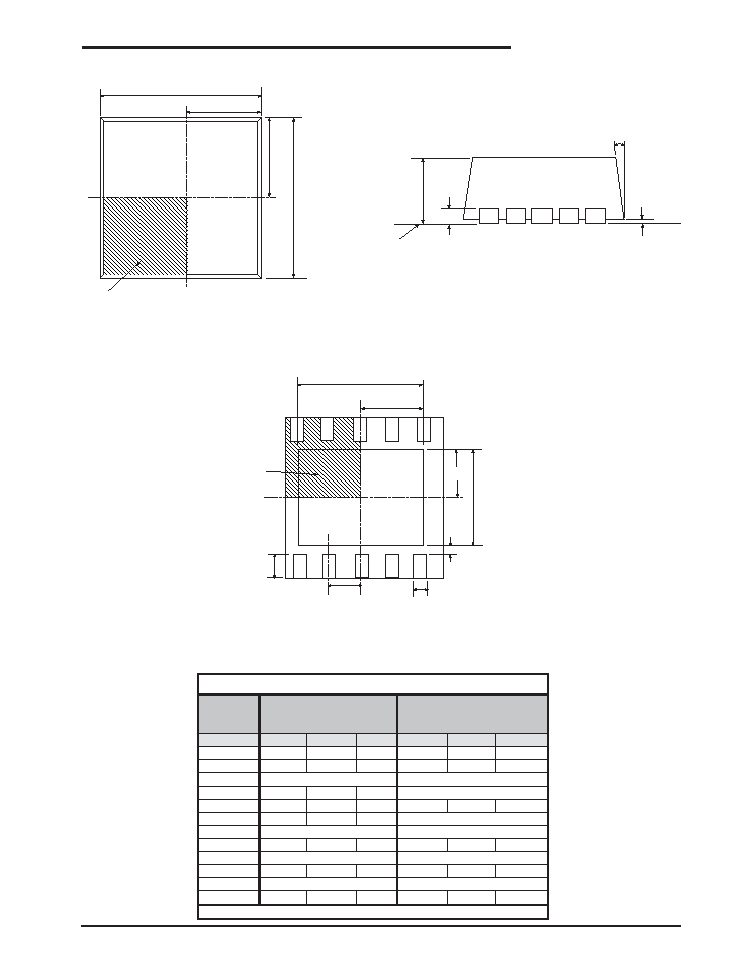
PACKAGE: 10 PIN DFN
MIN
NOM
MAX
MIN
NOM
MAX
A
0.80
0.90
1.00
0.032
0.036
0.039
A1
0.00
0.02
0.05
0.000
0.001
0.002
A3
K
0.20
-
-
0.008
-
-
ø
0º
-
14º
0º
-
14º
b
0.18
0.25
0.30
0.008
0.010
0.012
D
D2
2.20
-
2.70
0.087
-
0.106
E
E2
1.40
-
1.75
0.056
-
0.069
e
L
0.30
0.40
0.50
0.012
0.016
0.020
3x3 10 Pin DFN JEDEC MO-229 VARIATION VEED-5
Dimensions in Millimeters:
Controlling Dimension
Dimensions in Inches
Conversion Factor:
1 Inch = 25.40 mm
3.00 BSC
0.119 BSC
SYMBOL
SIPEX Pkg Signoff Date/Rev: JL Aug09-05 / RevA
0.20 REF
0.008 REF
0.119 BSC
3.00 BSC
0.020 BSC
0.50 BSC
ø
(A3)
A1
A
Seating Plane
SIDE VIEW
10
1
2
3
4
5
9
8
7
6
INDEX AREA
(D/2 x E/2)
BOTTOM VIEW
b
e
L
K
D2
E2
E2/2
D2/2
Pin1 Designator
to be within this
INDEX AREA
(D/2 x E/2)
TOP VIEW
D
E
E/2
D/2

12
Date: 6/20/06 Rev T SP7685, 1.2A Buck/BoostCharge Pump LED Driver © 2006 Sipex Corporation
Sipex Corporation reserves the right to make changes to any products described herein. Sipex does not assume any liability arising out of the
application or use of any product or circuit described herein; neither does it convey any license under its patent rights nor the rights of others.
Sipex Corporation
Headquarters and
Sales Office
233 South Hillview Drive
Milpitas, CA 95035
TEL: (408) 934-7500
FAX: (408) 935-7600
Part Number
Operating Temperature Range
Package Type
SP7685ER-L ............................................... -40°C to +85°C ....................................... (Lead Free) 10 Pin DFN
SP7685ER-L/TR ........................................ -40°C to +85°C ....................................... (Lead Free) 10 Pin DFN
/TR = Tape and Reel
Pack quantity is 3,000 for DFN.
ORDERING INFORMATION