 | ÐлекÑÑоннÑй компоненÑ: SP8538 | СкаÑаÑÑ:  PDF PDF  ZIP ZIP |
Äîêóìåíòàöèÿ è îïèñàíèÿ www.docs.chipfind.ru
SP8538DS/01
SP8538 Micropower Sampling 12-Bit A/D Converter
© Copyright 1999 Sipex Corporation
1
SP8538
Micropower Sampling 12-Bit A/D Converter
s
Low Cost
s
12-Bit Serial Sampling ADC
s
Guaranteed +1.0 LSB Max INL
s
Guaranteed No Missing Codes
s
8-Pin NSOIC Plastic Package
s
Low Power @ 250
µ
A including
Automatic Shutdown: 1nA(typ)
s
Programmable Input Configuration:
Full differential or 2 channel
single-ended
s
Single Supply 3.0V to 5.5V operation
s
Half Duplex Digital Serial Interface
s
Sample Rate: 40
µ
S
s
Pin Compatible Upgrade to LTC 1298
DESCRIPTION
The SP8538 is a very low power 12-Bit data acquisition chip. The SP8538 typically draws 250
µ
A
of supply current when sampling at 25 kHz. Supply current drops linearly as the sample rate is
reduced. The ADC automatically powers down when not performing conversions, drawing only
leakage current. The SP8538 is available in 8-Pin NSOIC packages, specified over Commercial
and Industrial temperature ranges. The SP8538 is best suited for Battery-Operated Systems,
Portable Data Acquisition Instrumentation, Battery Monitoring, and Remote Sensing
applications. The serial port allows efficient data transfer to a wide range of microprocessors and
microcontrollers over 3 or 4 wires.
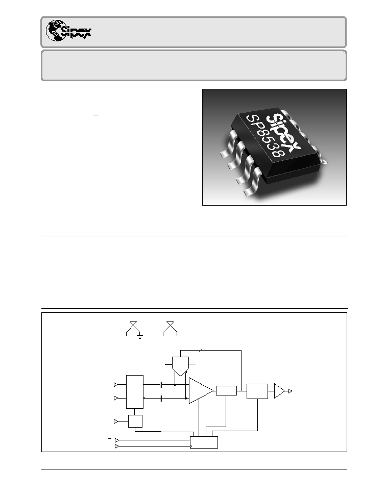
Internal
VCC
VCC
REFH
GND
REFL
DAC
REFL
Csample P
Csample N
INPUT
DATA
REG
CH0
CH1
DIN
SAR
PARALLEL TO
SERIAL SHIFT
REGISTER
12
CS
CLK
TIMING &
CONTROL LOGIC
Dout
REFH
COMPARATOR
MUX
SP8538 Block Diagram
SIGNAL PROCESSING EXCELLENCE
SP8538DS/01
SP8538 Micropower Sampling 12-Bit A/D Converter
© Copyright 1999 Sipex Corporation
2
ABSOLUTE MAXIMUM RATINGS
These are stress ratings only and functional operation of the device at
these ratings or any other above those indicated in the operation
sections of the specifications below is not implied. Exposure to absolute
maximum rating conditions for extended periods of time may affect
reliability.
(TA=+25°C unless otherwise noted) .....................................................
VCC to GND ................................................................................. 7.0V
Vin to GND .............................................................. -0.3 to VCC +0.3V
Digital input to GND ................................................ -0.3 to VCC +0.3V
Digital output to GND .............................................. -0.3 to VCC +0.3V
Operating Temperature Range
Commercial (J, K Version) ........................................... 0°C to 70°C
Industrial (A, B Version) .......................................... -40°C to +85°C
Lead Temperature (Solder 10Sec) ............................................ +300°C
Storage Temperature .................................................. -65°C to +150°C
Power Dissipation to 70°C ........................................................ 500mW
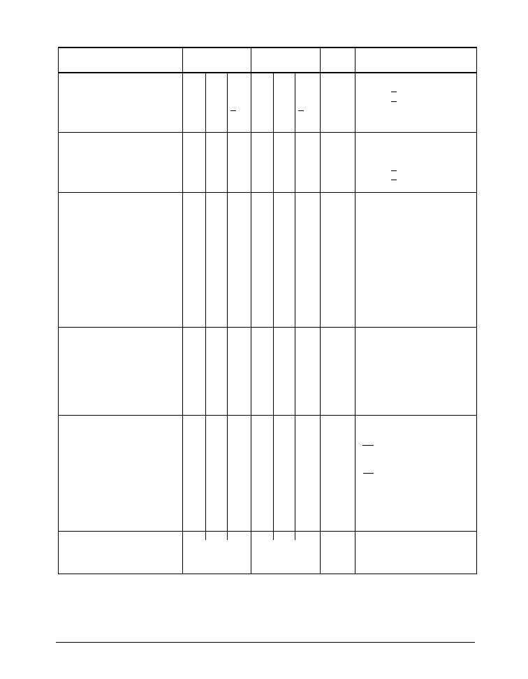
SPECIFICATIONS
Unless otherwise noted the following specifications apply for VCC=5V or 3.3V with limits applicable for Tmin to Tmax. Typical applies for Ta=25°C.
VCC=5.0V
VCC=3.3V
PARAMETERS
MIN. TYP. MAX. MIN. TYP. MAX.
UNITS
CONDITIONS
DC ACCURACY
Resolution
12
12
Bits
Integral Linearity
J,A
+0.6 +2.0
+0.6 +2.0
LSB
K,B
+0.6 +1.0
+0.6 +1.0
LSB
Differential Linearity Error
J,A
+0.75 +2.0
+0.75 +2.0
LSB
K,B
+0.75 +1.0
+0.75 +1.0
LSB
No Missing Codes
Gain Error
J,A
+2.0 +10
+2.0 +10
LSB
K,B
+2.0
+8
+2.0
+8
LSB
Offset Error
J,A
+1.5
+5
+3.0
+8
LSB
K,B
+1.5
+3
+3.0
+5
LSB
ANALOG INPUT
Input Signal FS Range
0
V
CC
0
V
CC
Input Impedance
On Channel
20
20
pF
In Parallel with 100m
100
100
M
Off Channel
3
3
pF
In Parallel with 100m
100
100
M
Input Bias Current
.001
1
.001
1
µ
A
Analog Input Range
-.05
V
CC
+.05 -.05
V
CC
+.05
Volts
MULTIPLEXER
Crosstalk (f
D
= Nyquist)
-90
-90
dB
Off to On Channel
Feedthrough (f
D
= Nyquist)
-90
-90
dB
Off to On Channel
f
D
= Disturbance
CONVERSION SPEED
Sample Time
1.5
1.5
clock
See Timing Diagrams
cycles
Conversion Time
12
12
clock
See Timing Diagrams
cycles
Complete Cycle
25
5.85
kHz
See Timing Diagrams
Clock Period
2.25
10.0
µ
S
See Timing Diagrams
Clock High Time
1.0
4.5
µ
S
See Timing Diagrams
Clock Low Time
1.0
4.5
µ
S
See Timing Diagrams
SP8538DS/01
SP8538 Micropower Sampling 12-Bit A/D Converter
© Copyright 1999 Sipex Corporation
3
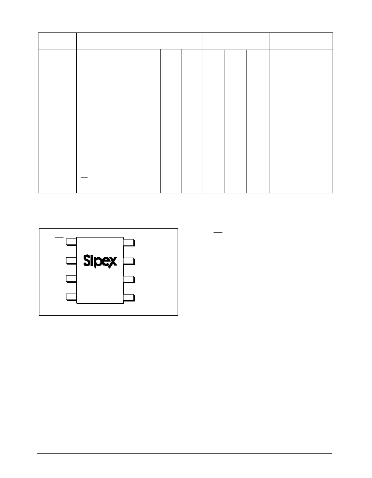
SPECIFICATIONS (cont.)
Unless otherwise noted the following specifications apply for VCC=5V or 3.3V with limits applicable for Tmin to Tmax. Typical applies for Ta=25°C.
VCC=5.0V
VCC=3.3V
PARAMETERS
MIN. TYP. MAX. MIN. TYP. MAX.
UNITS
CONDITIONS
DIGITAL INPUTS
Input Low Voltage, VIL
0.8
0.8
Volts
V
DD
=5V +5%
Input High Voltage, VIH
2.0
2.0
Volts
V
DD
=5V +5%
Input Current IIN
+2.0
+2.0
µ
A
Input Capacitance
3.0
3.0
pF
DIGITAL OUTPUTS
Data Format
Data Coding
See Timing Diagram
VOH
4.0
2.0
Volts
V
DD
=5V +5%, IOH=-0.4mA
VOL
0.4
0.4
Volts
V
DD
=5V +5%, IOH=+1.6mA
AC ACCURACY
Spurious free Dynamic
86
86
dB
For all FFT's
Range (SFDR)
(Full Differential Mode)
If V
CC
= 5V
fsample = 25kHz
fin = 12kHz
Total Harmonic Distortion (THD)
-83
-80
dB
Signal to Noise &
73
72
dB
If V
CC
= 3.3V
Distortion (SINAD)
fsample = 5.8kHz
fin = 2.8kHz
Signal to Noise (SNR)
73.5
72.5
dB
SAMPLING DYNAMICS
Acquisition Time to 0.01%
2
3.38
3
15.0
µ
s
-3dB Small Signal BW
5
4
MHz
Aperture Delay
20
30
nS
Aperture Jitter
150
150
pS
Common-Mode Rejection Ratio
70
80
70
80
dB
f
CM
= 12.5kHz @ 5 volts
2.8kHz @ 3.3 volts
POWER SUPPLIES
Volts
V
CC
+3.0 +5.0 +5.5 +3.0 +3.3 +5.5
Supply Current Operation Mode
250
400
150
300
µ
A
(CS=0) 25kHz, 5 volt conversion
rate. 5.8kHz 3.3 volts
Shutdown Mode
0.001 0.5
0.001 0.5
µ
A
(CS=1)
Power Dissipation
Operating Mode
1.25
2
0.5
0.99
mW
Shutdown Mode
2.5
1.7
µ
W
TEMPERATURE RANGE
Commercial
0° to +70°C
0° to +70°C
°C
Industrial
-40° to +85°C
-40° to +85°C
°C
Storage
-65° to +150°C
-65° to +150°C
°C
SP8538DS/01
SP8538 Micropower Sampling 12-Bit A/D Converter
© Copyright 1999 Sipex Corporation
4
PIN ASSIGNMENTS
Pin 1- CS
- Chip Select.
Pin 2- CH0 - Channel 0
Pin 3- CH1 - Channel 1
Pin 4- GND - Ground
Pin 5- D
IN
- Data In
Pin 6 - D
OUT
- Data Out
Pin 7- SCLK - Serial Clock
Pin 8- V
CC
/V
REF
- Supply & Reference Voltage
PIN DESCRIPTION
SPECIFICATIONS (cont.)
Recommended Operating Conditions
VCC=5.0V
VCC=3.3V
SYMBOL
PARAMETERS
MIN.
TYP.
MAX.
MIN.
TYP.
MAX.
UNITS
V
CC
Supply Voltage
+3.0
+5.0
+5.5
+3.0
+3.3
+5.5
Volts
f
CLK
Clock Frequency
444
100
kHz
t
CVC
Total Cycle Time
40
170
µ
S
t
hDI
Hold Time D
IN
After
50
0
50
0
nS
CLK^
t
suCS
Setup Time CSv
100
150
nS
Before CLK^
t
suDI
Setup Time, D
IN
100
10
150
nS
Stable Before CLK^
t
WHCLK
CLK High Time
1
4.5
µ
S
T
WHCLK
CLK Low Time
1
4.5
µ
S
T
WHCS
CS High Time between
100
150
nS
Data Transfers Cycles
CS
CH0
CH1
GND
V
CC
/V
REF
SCLK
D
OUT
D
IN
1
2
3
4
8
7
6
5
SP8538
SP8538DS/01
SP8538 Micropower Sampling 12-Bit A/D Converter
© Copyright 1999 Sipex Corporation
5
The device uses a capacitive DAC architecture
which provides the sampling behavior. This
results in full Nyquist performance at the
fastest throughput rate (25 KHz) the device is
capable of.
The power supply voltage is variable from 3.0V
to 5.5V which provides supply flexibility. At the
5.0V supply level, conversion plus sampling
time is 40
µ
S and supply current is 250
µ
A (1.25
mW). With a 3.3V supply the conversion plus
sampling time is 170
µ
S and current is reduced
to 150
µ
A (0.5 mW).
The device features automatic shutdown and
will shutdown to a +0.5
µ
A power level as CS
is brought high (de-selected). Power is
proportional to conversion duty cycle and
varies from 250
µ
A at 40
µ
S (Duty cycle =
100%) to 6.25
µ
a at 1.6 ms (Duty cycle = 2.5%).
Examples:
Conversion rate
I
CC
@ 5V
Duty Cycle
40
µ
S
250
µ
A
100%
80
µ
S
125
µ
A
50%
160
µ
S
62.5
µ
A
25%
DESCRIPTION
The SP8538 is a 12 bit sampling ADC with a
programmable two channel multiplexer and
serial data interface. The ADC samples and
converts 12 bits of data in 40
µ
S with a 5V
supply voltage applied. The SP8538 will also
operate at a 3.3V supply at 170
µ
S throughput.
The device automatically shuts down to a
+0.5
µ
A (MAX) level as soon as the chip is
deselected (CS=1). Serial data output is
available in an MSB first or LSB first format.
FEATURES
Two program bits, which are shifted into the
device prior to conversion, determine the input
configuration. In the single ended MUX
configuration the input signal will be applied to
either channel 0 or channel 1 and will be ground
referenced. The maximum full scale range is
VCC. In the full differential mode, the signal
will be applied between channel 0 and channel
1. The signals applied at each input may both
be dynamic. This is in contrast with pseudo
differential devices which must have input low
held at a constant level during conversion. The
converter will provide significant common mode
rejection when used in full differential manner.
Both inputs must remain between ground and
VCC for proper conversion.
0DRESSING
Mux Addressing
Channel #
GND
Comments
SGL/DIFF
ODD/SIGN
0
1
0
0
V
INH
V
INL
Full Differential Mode
0
1
V
INL
V
INH
1
0
V
INH
V
INL
Single Ended Mux Mode
1
1
V
INH
V
INL
INPUT VOLTAGE
INPUT VOLTAGE
OUTPUT
(V
INH
-V
INL
)*
AT V
CC
/V
REF
= 5V
CODE
0 LSB
0V
000000000000
1 LSB
0.00122V
000000000001
2048 LSB
2.5000V
100000000000
4094 LSB
4.9976V
111111111110
4095 LSB
4.9988V
111111111111
* See Mux Addressing Table for a definition of V
INH
- V
INL
.
ADC TRANSFER FUNCTION

SP8538DS/01
SP8538 Micropower Sampling 12-Bit A/D Converter
© Copyright 1999 Sipex Corporation
6
1.6 mS
6.25
µ
A
2.5%
The device can be configured such that it
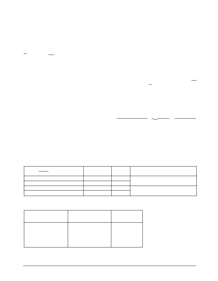
delivers serial data MSB first requiring 17 clock
periods for a full conversion. Alternately, the
device can be programmed to deliver 12 bits of
data MSB first, followed by the same 12 bits of
data LSB first. This sequence will require 28
clock periods to complete. Please refer to the
timing diagram.
Circuit Operation
The device will ignore any leading zeros
applied to the DIN pin even if CS is low. After
Chip Select Bar (CS) is brought low and the
START bit is clocked in to the converter, the
conversion sequence is initiated. Three
additional bits are clocked in immediately
following the START bit: SGL/DIFF, ODD/
SIGN & MSBF. The second and third bits
clocked in determine the MUX configuration
(see MUX addressing table). The fourth bit
determines the data output format (MSB first
or LSB first). Please refer to the timing diagram.
The SGL/DIFF bit when zero sets the input
MUX for full differential mode and when one,
sets the input MUX for single ended mode. The
ODD/SIGN bit when zero sets channel zero as
the positive input (ground referred for single
ended operation and referred to channel one in
differential mode). With the ODD/SIGN bit one,
channel one will be the positive input (ground
referred for single ended operation and referred
to channel zero in differential mode).
With MSBF set to one, the output data stream
will be MSB through LSB, with MSBF set to
zero the output data stream will be MSB through
LSB followed by the same data in LSB through
MSB format.
The SP8538 is a SAR converter with full
differential multiplexed front end, capacitive
DAC, precision comparator, Successive
Approximations Register, control logic and data
output register. After the input is sampled and
held the conversion process begins. The DAC
MSB is set and its output is compared with the
signal input, if the DAC output is less than the
input, the comparator outputs a one which is
latched into the SAR and simultaneously made
available at the ADC serial output pin. Each bit
is tested in a similar manner until the SAR
contains a code which represents the signal input
to within +1/2 LSB. During this process the SAR
content has been shifted out of the ADC serially.
If the MSB first format was chosen, the data will
appear at the DOUT pin MSB through LSB in 17
clock periods. If the LSB first format was chosen
then during conversion the data will appear at the
DOUT pin just as before (MSB through LSB) but
the LSB will be followed by D1, D2 through the
MSB. This sequence will require 28 clock
periods. Note that the Chip Select Bar pin must
be toggled high between conversions. The DOUT
pin will be in a high impedance state whenever
Chip Select Bar is high. After Chip Select Bar
has been toggled and brought low again, the
converter is ready to accept another START bit
and begin a new conversion.
Full Differential Sampling
The SP8538 can be configured for single-ended
sampling (i.e. CH0-ground or CH1-ground) or
full differential sampling (CH0-CH1 or
CH1-CH0). In the full differential sampling
configuration, both inputs are sampled and held
simultaneously. Because of the balanced
differential sampling, dynamic common mode
noise riding along the input signal is cancelled
above and beyond DC noise. This is a significant
improvement over psuedo-differential sampling
schemes, where the low side of the input must
remain constant during the conversion, and
therefore only DC noise (i.e. signal offset) is
cancelled. If AC common mode noise is left to
be converted along with the differental
component, the output signal will be degraded.
Full differential sampling allows flexibility in
converting the input signal. If the signal
low- side is already tied to a ground elsewhere
in the system, it can be hardwired to the low
side channel (i.e. CH0 or CH1) which acts as a
signal ground sense, breaking a potential ground
loop. It is also possible to drive the inputs bal-
anced differential, as long as both inputs are
within the power rails. In this configuration, both
the high and low signals have the same
impedance looking back to ground, and
therefore pick up the same noise along the
physical path from signal source (i.e. sensor,
transducer, battery) to converter. This noise
becomes common mode, and is cancelled out
SP8538DS/01
SP8538 Micropower Sampling 12-Bit A/D Converter
© Copyright 1999 Sipex Corporation
7
by the differential sampling of the SP8538.
Layout Considerations
To preserve the high resolution and linearity of
the SP8538 attention must be given to circuit
board layout, ground impedance and bypassing.
A circuit board layout which includes separate
analog and digital ground planes will prevent
the coupling of noise into sensitive converter
circuits and will help to preserve the dynamic
performance of the device. In single ended
mode, the analog input signal should be
referenced to the ground pin of the converter.
This prevents any voltage drops that occur in
the power supply's common return from
appearing in series with the input signal.
In full differential mode, the high and low side
board traces should run close to each other, with
the same layout. This will insure that any noise
coupling will be common mode, and cancelled
by the converters (patent pending) full differential
architecture.
If separate analog and digital ground planes are
not possible, care should be used to prevent
coupling between analog and digital signals. If
analog and digital lines must cross, they should
CS
CLK
DIN
DOUT
CS
CLK
DIN
DOUT
X
X
POWER UP
SAMPLE
CONVERT
1
4
10
16
X
START O/S
S/D LSBFN
HI-Z
"0"
D1
20
D0 D1
POWER DOWN
28
X
D11
HI-Z
X
LSB FIRST CONVERSION
D11
X
X
POWER UP
SAMPLE
CONVERT
1
4
10
16
X
START O/S
S/D MSBF
HI-Z
"0"
D1 D0
POWER DOWN
X
HI-Z
X
D11
17
MSB FIRST CONVERSION
do so at right angles. Parallel analog and digital
lines should be separated by a circuit board trace
which is connected to common.
The SP8538 VCC pin is also the reference pin
for the device. This means that noise on the VCC
pin will be proportionally represented as noise
in the converters output data. A noise signal of
1.22mV (at a 5V supply) will produce 1 LSB of
error in the output data. The VCC pin should be
bypassed to the ground pin with a parallel
combination of a 6.8
µ
F tantalum and a 0.1
µ
F
ceramic capacitor. To maintain maximum
system accuracy, the supply connected to the
VCC pin should be well isolated from digital
supplies and wide load variations. A separate
conductor from the supply regulator to the A/D
converter will limit the effects of digital switching
elsewhere in the system. Power supply noise can
degrade the converters performance. Especially
corrupting are noise and spikes from a switching
power supply.
To avoid introducing distortion when driving the
A/D converter input, the input signal source
should be able to charge the SP8538's
equivalent 20 pF of input capacitance from zero
volts to the signal level in 1.5 clock periods.
SP8538 Timing Diagram
SP8538DS/01
SP8538 Micropower Sampling 12-Bit A/D Converter
© Copyright 1999 Sipex Corporation
8
Icc versus Sampling Rate
(clock rate = 100kHz)
Vcc = 3.3V
Icc versus Sampling Rate
(clock rate = 500kHz)
Vcc = 5V
Icc (
µ
A)
Icc (
µ
A)
conversion time (
µ
s)
Vcc = 5.00V
Vcc = 3.30V
Input CMRR,
Vcc = 5V
FFT 20 dB/div
conversion time (
µ
s)
Spectral Density dB
CMRR (dB)
Frequency
SNR = -73.31 dB
THD = -78.53 dB
SINAD = -72.17 dB
SFDR = -80.15 dB
Vin amp = -0.02 dB
Input CMFrequency
0
13.9Kz
0
4095
0
4095
SP8538DS/01
SP8538 Micropower Sampling 12-Bit A/D Converter
© Copyright 1999 Sipex Corporation
9
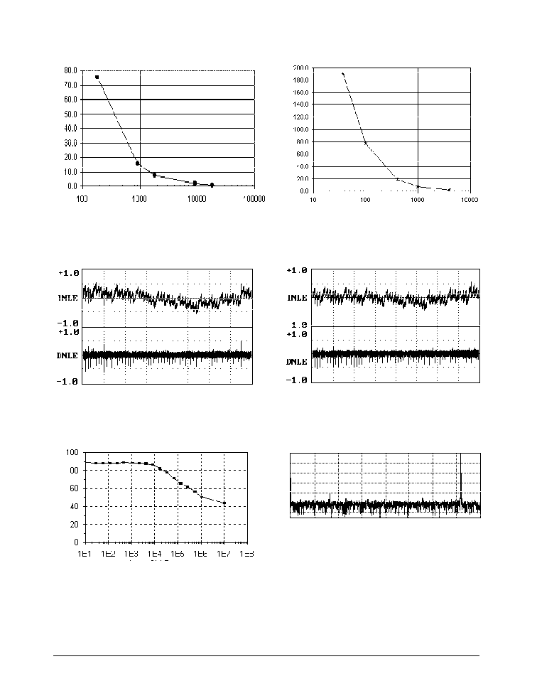
Icc vs. Temperature
Gain Error vs. Temperature
temperature (C)
µ
A
temperature (C)
LSB
Offset vs. Temperature
Spurious Free Dynamic Range
temperature (C)
LSB
Frequency
dB
SINAD
Signal to Noise Ratio
Frequency
dB
Frequency
dB
Total Harmonic Distortion
Frequency
dB
SP8538DS/01
SP8538 Micropower Sampling 12-Bit A/D Converter
© Copyright 1999 Sipex Corporation
10
D
ALTERNATE
END PINS
(BOTH ENDS)
D1 = 0.005" min.
(0.127 min.)
E
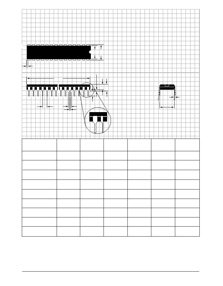
PACKAGE: PLASTIC
DUALINLINE
(NARROW)
DIMENSIONS (Inches)
Minimum/Maximum
(mm)
A = 0.210" max.
(5.334 max).
E1
C
Ø
L
A2
A1 = 0.015" min.
(0.381min.)
B
B1
e = 0.100 BSC
(2.540 BSC)
e
A
= 0.300 BSC
(7.620 BSC)
A2
B
B1
C
D
E
E1
L
Ø
0.115/0.195
(2.921/4.953)
0.014/0.022
(0.356/0.559)
0.045/0.070
(1.143/1.778)
0.008/0.014
(0.203/0.356)
0.735/0.775
(18.669/19.685)
0.300/0.325
(7.620/8.255)
0.240/0.280
(6.096/7.112)
0.115/0.150
(2.921/3.810)
0°/ 15°
(0°/15°)
0.115/0.195
(2.921/4.953)
0.014/0.022
(0.356/0.559)
0.045/0.070
(1.143/1.778)
0.008/0.014
(0.203/0.356)
0.355/0.400
(9.017/10.160)
0.300/0.325
(7.620/8.255)
0.240/0.280
(6.096/7.112)
0.115/0.150
(2.921/3.810)
0°/ 15°
(0°/15°)
22PIN
8PIN
14PIN
16PIN
0.115/0.195
(2.921/4.953)
0.014/0.022
(0.356/0.559)
0.045/0.070
(1.143/1.778)
0.008/0.014
(0.203/0.356)
1.145/1.155
(29.083/29.337)
0.300/0.325
(7.620/8.255)
0.240/0.280
(6.096/7.112)
0.115/0.150
(2.921/3.810)
0°/ 15°
(0°/15°)
0.115/0.195
(2.921/4.953)
0.014/0.022
(0.356/0.559)
0.045/0.070
(1.143/1.778)
0.008/0.014
(0.203/0.356)
0.780/0.800
(19.812/20.320)
0.300/0.325
(7.620/8.255)
0.240/0.280
(6.096/7.112)
0.115/0.150
(2.921/3.810)
0°/ 15°
(0°/15°)
18PIN
0.115/0.195
(2.921/4.953)
0.014/0.022
(0.356/0.559)
0.045/0.070
(1.143/1.778)
0.008/0.014
(0.203/0.356)
0.880/0.920
(22.352/23.368)
0.300/0.325
(7.620/8.255)
0.240/0.280
(6.096/7.112)
0.115/0.150
(2.921/3.810)
0°/ 15°
(0°/15°)
20PIN
0.115/0.195
(2.921/4.953)
0.014/0.022
(0.356/0.559)
0.045/0.070
(1.143/1.778)
0.008/0.014
(0.203/0.356)
0.980/1.060
(24.892/26.924)
0.300/0.325
(7.620/8.255)
0.240/0.280
(6.096/7.112)
0.115/0.150
(2.921/3.810)
0°/ 15°
(0°/15°)
SP8538DS/01
SP8538 Micropower Sampling 12-Bit A/D Converter
© Copyright 1999 Sipex Corporation
11
D
E
H
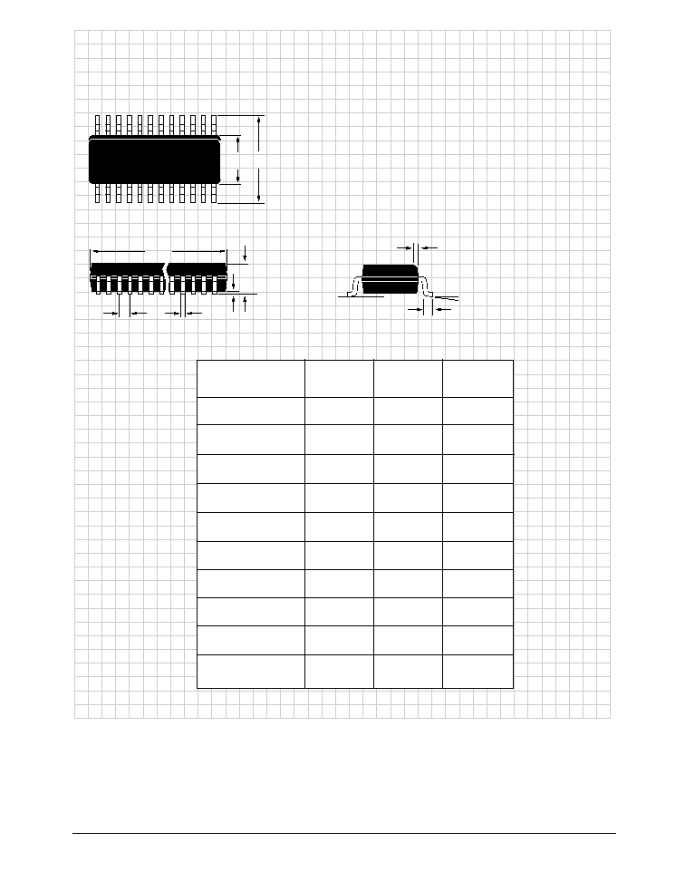
PACKAGE: PLASTIC
SMALL OUTLINE (SOIC)
(NARROW)
DIMENSIONS (Inches)
Minimum/Maximum
(mm)
8PIN
A
A1
Ø
L
B
e
h x 45°
A
A1
B
D
E
e
H
h
L
Ø
0.053/0.069
(1.346/1.748)
0.004/0.010
(0.102/0.249
0.014/0.019
(0.35/0.49)
0.189/0.197
(4.80/5.00)
0.150/0.157
(3.802/3.988)
0.050 BSC
(1.270 BSC)
0.228/0.244
(5.801/6.198)
0.010/0.020
(0.254/0.498)
0.016/0.050
(0.406/1.270)
0°/8°
(0°/8°)
14PIN
0.053/0.069
(1.346/1.748)
0.004/0.010
(0.102/0.249)
0.013/0.020
(0.330/0.508)
0.337/0.344
(8.552/8.748)
0.150/0.157
(3.802/3.988)
0.050 BSC
(1.270 BSC)
0.228/0.244
(5.801/6.198)
0.010/0.020
(0.254/0.498)
0.016/0.050
(0.406/1.270)
0°/8°
(0°/8°)
16PIN
0.053/0.069
(1.346/1.748)
0.004/0.010
(0.102/0.249)
0.013/0.020
(0.330/0.508)
0.386/0.394
(9.802/10.000)
0.150/0.157
(3.802/3.988)
0.050 BSC
(1.270 BSC)
0.228/0.244
(5.801/6.198)
0.010/0.020
(0.254/0.498)
0.016/0.050
(0.406/1.270)
0°/8°
(0°/8°)
SP8538DS/01
SP8538 Micropower Sampling 12-Bit A/D Converter
© Copyright 1999 Sipex Corporation
12
ORDERING INFORMATION
Model ........................................................ Linearity (LSB) ..................... Temperature Range ............................................................... Package
SP8538BN ..........................................................
±
1.0 .................................... 40°C to +85°C .............................................. 8-pin, 0.3" Plastic DIP
SP8538KN ..........................................................
±
1.0 ..................................... 0°C to +70°C ............................................... 8-pin, 0.3" Plastic DIP
SP8538BS ..........................................................
±
1.0 .................................... 40°C to +85°C ......................................... 8-pin, 0.15" Plastic SOIC
SP8538KS ..........................................................
±
1.0 ..................................... 0°C to +70°C .......................................... 8-pin, 0.15" Plastic SOIC
SP8538AN ..........................................................
±
2.0 .................................... 40°C to +85°C .............................................. 8-pin, 0.3" Plastic DIP
SP8538JN ...........................................................
±
2.0 ..................................... 0°C to +70°C ............................................... 8-pin, 0.3" Plastic DIP
SP8538AS ..........................................................
±
2.0 .................................... 40°C to +85°C ......................................... 8-pin, 0.15" Plastic SOIC
SP8538JS ...........................................................
±
2.0 ..................................... 0°C to +70°C .......................................... 8-pin, 0.15" Plastic SOIC
Sipex Corporation reserves the right to make changes to any products described herein. Sipex does not assume any liability arising out of the
application or use of any product or circuit described hereing; neither does it convey any license under its patent rights nor the rights of others.
Corporation
SIGNAL PROCESSING EXCELLENCE
Sipex Corporation
Headquarters and
Sales Office
22 Linnell Circle
Billerica, MA 01821
TEL: (978) 667-8700
FAX: (978) 670-9001
e-mail: sales@sipex.com
Sales Office
233 South Hillview Drive
Milpitas, CA 95035
TEL: (978) 934-7500
FAX: (978) 935-7600
Far East:
JAPAN:
Nippon Sipex Corporation
Yahagi No. 2 Building
3-5-3 Uchikanda, Chiyoda-ku
Tokyo 101
TEL: 81.3.3256.0577
FAX: 81.3.3256.0621
European Sales Offices:
ENGLAND:
Sipex Corporation
2 Linden House
Turk Street
Alton Hampshire GU34 IAN
England
TEL: 44-1420-549527
FAX: 44-1420-542700
e-mail: mikeb@sipex.co.uk
GERMANY:
Sipex GmbH
Gautinger Strasse 10
82319 Starnberg
TEL: 49.81.51.89810
FAX: 49.81.51.29598
e-mail: sipex-starnberg@t-online.de
Please consult the factory for pricing and availability on a Tape-On-Reel option.