 | –≠–ª–µ–∫—Ç—Ä–æ–Ω–Ω—ã–π –∫–æ–º–ø–æ–Ω–µ–Ω—Ç: SP9504S | –°–∫–∞—á–∞—Ç—å:  PDF PDF  ZIP ZIP |
SP9504DS/03
SP9504 Quad, 12-Bit, Voltage Output D/A Converter
© Copyright 2000 Sipex Corporation
1
SP9504
Quad, 12≠Bit, Voltage Output D/A Converter
s
Low Cost
s
Four 12≠Bit DAC's on a Single Chip
s
Low Power -- 80 mW (20mW/DAC)
s
Double-Buffered Inputs
s
±
5V Supply Operation
s
Voltage Outputs,
±
4.5V Range
s
Midscale Preset, Zero Volts Out
s
Guaranteed +0.5 LSB Max INL
s
Guaranteed +0.75 LSB Max DNL
s
2MHz 4-Quadrant Multiplying Bandwidth
s
28≠pin SOIC and Plastic DIP
Packages
s
Either 12 or 8 bit
µ
P bus
DESCRIPTION
The SP9504 is a low power replacement for the popular SP9345, Quad 12-Bit Digital-to-Analog
Converter. It features +4.5V output swings when using
±
5 volt supplies. The converter is double-
buffered for easy microprocessor interface. Each 12-bit DAC is independently addressable and
all DAC
S
may be simultaneously updated using a single transfer command. The output settling-
time is specified at 4
µ
s. The SP9504 is available in 28≠pin SOIC and plastic DIP packages,
specified over commercial temperature range.
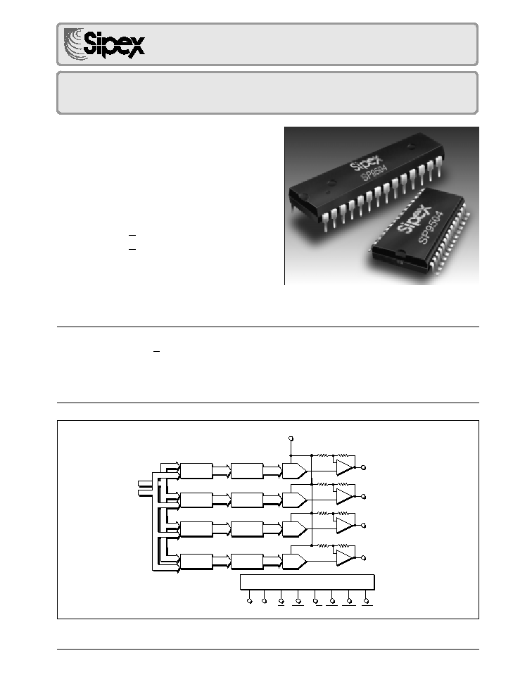
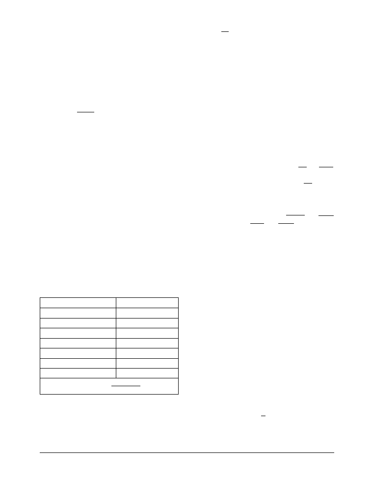
DAC
DAC
LATCH
LATCH
LATCH
LATCH
8 MSB's
4 LSB's
≠
+
≠
+
VOUT3
VOUT4
DAC
DAC
LATCH
LATCH
LATCH
LATCH
Ref In
≠
+
≠
+
VOUT1
VOUT2
A1
CS
WR1 B1/B2 WR2 XFER CLR
A0
CONTROL LOGIC
INPUT
REGISTERS
DAC
REGISTERS
DATA
INPUTS
Æ
SP9504DS/03
SP9504 Quad, 12-Bit, Voltage Output D/A Converter
© Copyright 2000 Sipex Corporation
2
ABSOLUTE MAXIMUM RATINGS
These are stress ratings only and functional operation of the device
at these or any other above those indicated in the operation
sections of the specifications below is not implied. Exposure to
absolute maximum rating conditions for extended periods of time
may affect reliability.
V
DD
- GND .................................................................... -0.3V, +6.0V
V
SS
- GND .................................................................... +0.3V, -6.0V
V
DD
- V
SS
......................................................................................................................
-0.3V, +12.0V
V
REF
..................................................................................... V
SS
, V
DD
D
IN
....................................................................................... V
SS
, V
DD
Power Dissipation
Plastic DIP .......................................................................... 375mW
(derate 7mW/
∞
C above +70
∞
C)
Small Outline ...................................................................... 375mW
(derate 7mW/∞C above +70∞C)
SPECIFICATIONS
(Typical at 25∞C;T
MIN
T
A
T
M AX
; V
DD
= +5V, V
SS
= -5V, V
REF
= +3V; CMOS logic level digital inputs; specifications apply to all grades unless otherwise noted.)
PARAMETER
MIN.
TYP.
MAX.
UNITS
CONDITIONS
DIGITAL INPUTS
Logic Levels
V
IH
2.4
Volts
V
IL
0.8
Volts
4 Quad, Bipolar Coding
Offset Binary
REFERENCE INPUT
Voltage Range
+3
+4.5
Volts
Note 5
Input Resistance
1.5
2.2
k
D
IN
= 1,877; code dependent
ANALOG OUTPUT
Gain
≠K
+0.5
+2.0
LSB
V
REF
= +3V; Note 3
≠J
+1.0
+4.0
LSB
V
REF
= +3V; Note 3
≠K, ≠J
+1.0
+5.0
LSB
V
REF
= +4.5V; Note 3
Initial Offset Bipolar
+0.25
+3.0
LSB
D
IN
= 2,048
Voltage Range Bipolar
+3.0
+4.5
Volts
Output Current
+5.0
mA
V
REF
= +3V
+0.5
mA
V
REF
= +4.5V
STATIC PERFORMANCE
Resolution
12
Bits
Integral Linearity
≠K
+0.25
+0.5
LSB
V
REF
= +3V; Note 3
≠J
+0.5
+1.0
LSB
V
REF
= +3V; Note 3
≠K, ≠J
+0.5
+3.0
LSB
V
REF
= +4.5V; Note 3
Differential Linearity
-K
+0.25
+0.75
LSB
-J
+0.25
+1.0
LSB
Monotonicity
Guaranteed
DYNAMIC PERFORMANCE
Multiplying Bandwidth
2
MHz
Settling Time
Small Signal
0.5
µ
s
to 0.012%
Full Scale
4
µ
s
to 0.012%
Slew Rate
4
V/
µ
s
SP9504DS/03
SP9504 Quad, 12-Bit, Voltage Output D/A Converter
© Copyright 2000 Sipex Corporation
3
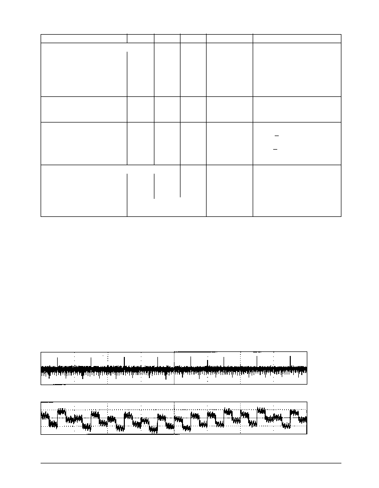
DNLE, INLE plots
+0.25 lsb
DNLE
-0.25 lsb
+0.25 lsb
INLE
-0.25 lsb
0
CODE 4095
Vref = 3V
SPECIFICATIONS (CONTINUED)
(Typical at 25∞C; T
MIN
T
A
T
MAX
; V
DD
= +5V, V
SS
= -5V, V
REF
= +3V; CMOS logic level digital inputs; specifications apply to all grades unless otherwise noted.)
PARAMETER
MIN.
TYP.
MAX.
UNITS
CONDITIONS
SWITCHING CHARACTERISTICS
t
DS
Data Set Up Time
140
100
ns
to rising edge of WR1
t
DN
Data Hold Time
0
ns
Figure 4
t
WR
Write Pulse Width
140
100
ns
t
XFER
Transfer Pulse Width
140
100
ns
t
WC
Total Write Command
280
200
ns
STABILITY
Gain
15
ppm/∞C
t
MIN
to t
MAX
Bipolar Zero
15
ppm/∞C
t
MIN
to t
MAX
POWER REQUIREMENTS
Note 5
V
DD
+5V, +3%; Note 4, 5
≠J, ≠K
8
11
mA
V
SS
-5V, +3%; Note 4, 5
≠J, ≠K
8
11
mA
Power Dissipation
80
mW
ENVIRONMENTAL AND MECHANICAL
Operating Temperature
≠J, ≠K
0
+70
∞
C
Storage
≠60
+150
∞
C
Package
≠_P
28≠pin Plastic DIP
≠_S
28≠pin SOIC
Notes:
1.
Integral Linearity, for the SP9504, is measured as the arithmetic mean value of the magnitudes of
the greatest positive deviation and the greatest negative deviation from the theoretical value for any
given input condition.
2.
Differential Linearity is the deviation of an output step from the theoretical value of 1 LSB for any two
adjacent digital input codes.
3.
1 LSB = 2*V
REF
/4,096.
4.
V
REF
= 0V.
5.
The following power up sequence is recommended to avoid latch up: V
SS
(-5V), Vdd (+5V), REF IN.
SP9504DS/03
SP9504 Quad, 12-Bit, Voltage Output D/A Converter
© Copyright 2000 Sipex Corporation
4
PINOUT -- 28≠PIN PLASTIC DIP & SOIC
V
OUT4
V
SS
V
DD
CLR
REF IN
GND
B1/B2
A
0
A
1
XFER
WR2
WR1
CS
V
OUT1
V
OUT3
DB
0
DB
1
DB
2
DB
3
DB
4
DB
5
DB
6
DB
7
DB
8
DB
9
DB
10
DB
11
V
OUT2
1
2
3
4
5
6
7
8
9
10
11
12
13
14
28
27
26
25
24
23
22
21
20
19
18
17
16
15
SP9504
PIN ASSIGNMENTS
Pin 1 -- V
OUT 4
-- Voltage Output from DAC4.
Pin 2 -- V
SS
-- ≠5V Power Supply Input.
Pin 3 -- V
DD
-- +5V Power Supply Input.
Pin 4 -- CLR -- Clear. Gated with WR2 (pin
11). Active low. Clears all DAC outputs to 0V.
Pin 5 -- REF IN -- Reference Input for DACs.
Pin 6 -- GND -- Ground.
Pin 7 -- B1/B2 -- Byte 1/Byte 2 -- Selects
Data Input Format. A logic "1" on pin 7 selects
the 12≠bit mode, and all 12 data bits are pre-
sented to the DAC(s) unchanged; a logic "0"
selects the 8≠bit mode, and the four LSBs are
connected to the four MSBs, allowing an 8≠bit
MSB≠justified interface.
Pins 8 and 9 -- A
0
& A
1
-- Address for DAC
Selection. A
1
/A
0
= 0/0 = DAC1; 0/1 = DAC2; 1/
0 = DAC3; 1/1 = DAC4.
Pin 10 -- XFER -- Transfer. Gated with WR2
(pin 11); loads all DAC registers simultaneously.
Active low.
Pin 11 -- WR2 -- Write Input 2 -- In conjunc-
tion with XFER (pin 10), controls the transfer of
data from the input registers to the DAC regis-
ters. In conjunction with CLR (pin 4), the DAC
registers are forced to 1000 0000 0000 and the
DAC outputs will settle to 0V. Active low.
Pin 12 -- WR1 -- Write Input1 -- In conjunc-
tion with CS (pin 13), enables input register
selection, and controls the transfer of data from
the input bus to the input registers. Active low.
Pin 13 -- CS -- Chip Select -- Enables writing data
to input registers and/or transferring data from input
bus to DAC registers. Active low.
Pin 14 -- V
OUT1
-- Voltage Output from DAC1.
Pin 15 -- V
OUT2
-- Voltage Output from DAC2.
Pin 16 -- DB
11
-- Data Bit 11; Most Significant Bit.
Pin 17 -- DB
10
-- Data Bit 10.
Pin 18 -- DB
9
-- Data Bit 9.
Pin 19 -- DB
8
-- Data Bit 8.
Pin 20 -- DB
7
-- Data Bit 7.
Pin 21 -- DB
6
-- Data Bit 6.
Pin 22 -- DB
5
-- Data Bit 5.
Pin 23 -- DB
4
-- Data Bit 4.
Pin 24 -- DB
3
-- Data Bit 3.
Pin 25 -- DB
2
-- Data Bit 2.
Pin 26 -- DB
1
-- Data Bit 1.
Pin 27 -- DB
0
-- Data Bit 0; LSB
Pin 28 -- V
OUT3
-- Voltage Output from DAC3.
SP9504DS/03
SP9504 Quad, 12-Bit, Voltage Output D/A Converter
© Copyright 2000 Sipex Corporation
5
FEATURES
The SP9504 is a low≠power replacement for the
popular SP9345, Quad 12-Bit Digital-to-Analog
Converter. This Quad, Voltage Output, 12-Bit Digi-
tal-to-Analog Converter features
±
4.5V output swings
when using
±
5 volt supplies. The input coding format
used is standard offset binary, Table 1.
The converter utilizes double-buffering on each of the
12 parallel digital inputs, for easy microprocessor
interface. Each 12-bit DAC is independently addres-
sable and all DAC
S
may be simultaneously updated
using a single XFER command. The output settling-
time is specified at 4
µ
s to full 12≠bit accuracy when
driving a 5Kohm, 50pF load combination. The
SP9504, Quad 12-Bit Digital-to-Analog Converter is
ideally suited for applications such as ATE, process
controllers, robotics, and instrumentation. The SP9504
is available in 28≠pin plastic DIP or SOIC packages,
specified over the commercial (0
∞
C to +70
∞
C)
temperature range.
THEORY OF OPERATION
The SP9504 consists of five main functional blocks
-- input data multiplexer, data registers, control logic,
four 12-bit D/A converters, and four bipolar output
voltage amplifiers. The input data multiplexer is
designed to interface to either 12- or 8-bit micropro-
cessor data busses. The input data format is controlled
by the B1/B2 signal -- a logic "1" selects the 12-bit
mode, while a logic "0" selects the 8-bit mode. In the
12-bit mode the data is transferred to the input registers
without changes in its format. In the 8-bit mode, the
four least significant bits (LSBs) are connected to the
four most significant bits (MSBs), allowing an 8-bit
MSB-justified interface. All data inputs are enabled
using the CS signal in both modes. The digital inputs
are designed to be both TTL and 5V CMOS compat-
ible.
In order to reduce the DAC full scale output sensitivity
to the large weighting of the MSB's found in conven-
tional R-2R resistor ladders, the 3 MSB's are decoded
into 8 equally weighted levels. This reduces the
contribution of each bit by a factor of 4, thus, reducing
the output sensitivity to mismatches in resistors and
switches by the same amount. Linearity errors and
stability are both improved for the same reasons.
Each D/A converter is separated from the data bus by
two registers, each consisting of level-triggered latches,
Figure 1. The first register (input register) is 12-bits
wide. The input register is selected by the address
input A
0
and A
1
, and is enabled by the CS and WR1
signals. In the 8-bit mode, the enable signal to the 8
MSB's is disabled by a logic low on B1/B2 to allow
the 4 LSB's to be updated. The second register (DAC
register), accepts the decoded 3 MSB's plus the 9
LSB's. The four DAC registers are updated simulta-
neously for all DAC's using the XFER and WR2
signals. Using the CLR and WR2 signals or the
power-on-reset, (enabled when the power is switched
on) the DAC registers are set to 1000 0000 0000 and
the DAC outputs will settle to 0V.
Using the control logic inputs, the user has full control
of address decoding, chip enable, data transfer and
clearing of the DAC's. The control logic inputs are
level triggered, and like the data inputs, are TTL and
CMOS compatible. The truth table (Table 2) shows
the appropriate functions associated with the states of
the control logic inputs.
The DACs themselves are implemented with a preci-
sion thin≠film resistor network and CMOS transmis-
sion gate switches. Each D/A converter is used to
convert the 12≠bit input from its DAC register to a
precision voltage.
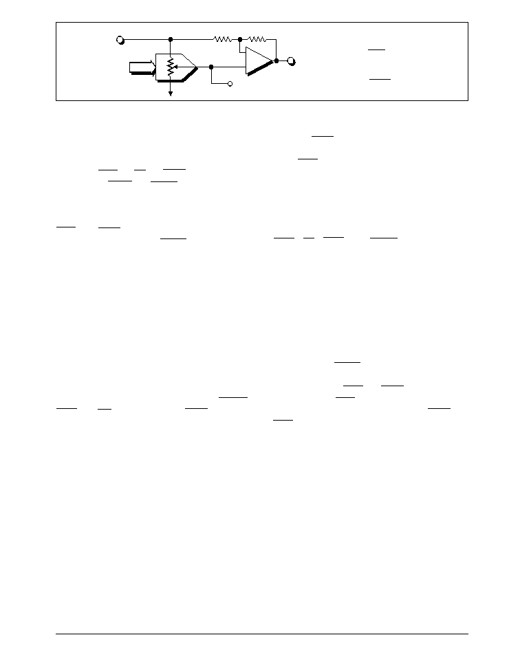
The bipolar voltage output of the SP9504 is created
on-chip from the DAC Voltage Output (V
DAC
) by
using an operational amplifier and two feedback
resistors connected as shown in Figure 2. This
configuration produces a +4.5V bipolar output range
with standard offset binary coding.
INPUT
OUTPUT
MSB
LSB
1111
1111
1111
VREF - 1 LSB
1111
1111
1110
VREF - 2 LSB
1000
0000
0001
0 + 1 LSB
1000
0000
0000
0
0000
0000
0001
-VREF + 1 LSB
0000
0000
0000
-VREF
1 LSB =
Table 1. Offset Binary Coding
2V
REF
2
12
SP9504DS/03
SP9504 Quad, 12-Bit, Voltage Output D/A Converter
© Copyright 2000 Sipex Corporation
6
A
1
A
0
CS
WR1
B1/B2
WR2
XFER
CLR
FUNCTION
0
0
1
1
X
X
Address DAC 1 and load input register
0
0
0
1
X
X
Address DAC 1 and load 4 LSBs
0
1
1
1
X
X
Address DAC 2 and load input register
0
1
0
1
X
X
Address DAC 2 and load 4 LSBs
1
0
1
1
X
X
Address DAC 3 and load input register
1
0
0
1
X
X
Address DAC 3 and load 4 LSBs
1
1
1
1
X
X
Address DAC 4 and load input register
1
1
0
1
X
X
Address DAC 4 and load 4 LSBs
X
X
**
**
X
1
Transfer data from input registers to DAC registers
X
X
X
X
X
1
Sets all DAC output voltages to 0V
X
X
1
1
X
0
0
Temporarily force all DAC output voltages to 0V,
while CLR is low
X
X
1
X
X
X
X
X
Invalid state with any other control line active
X
X
X
1
X
X
X
X
Invalid state with any other control line active
X = Don't care; ** = Don't care; however, CS and WR1 = 1 will inhibit changes to the input registers.
To load a 12-bit word to the input register of
each DAC, using an 8-bit data bus, the sequence
is as follows:
1) Set XFER=1, B1/B2=1, CLR=1, WR1=1,
WR2=1, CS=1.
2) Set D11 through D4 to the 8 MSB's of the
desired digital input code.
3) Load the 8 MSB's of the digital word to
the selected input register by cycling WR1
and CS through the "1" -- "0" -- "1"
sequence.
4) Reset B1/B2 from "1" ---- "0"
5) Set D11 (MSB) through D8 to the 4 LSB's
of the digital input code.
6) Load the 4 LSB's by cycling WR1 and CS
through the "1" -- "0" -- "1" sequence.
Figure 1. Detailed Block Diagram (only one DAC shown)
USING THE SP9504 WITH
DOUBLE-BUFFERED INPUTS
Loading Data
To load a 12-bit word to the input register of
each DAC, using a 12-bit data bus, the sequence
is as follows:
1) Set XFER=1, B1/B2=1, CLR=1, WR1=1,
WR2=1, CS=1.
2) Set A
1
and A
0
(the DAC address) to the
desired DAC -- 0,0 = DAC
1
; 0,1 = DAC
2
1,0 = DAC
3
; 1,1 = DAC
4
.
3) Set D11 (MSB) through D0 (LSB) to the
desired digital input code.
4) Load the word to the selected DAC by
cycling WR1 and CS through the follow-
ing sequence:
"1" -- "0" -- "1"
5) Repeat sequence for each input register.
DAC
3 TO 7
DECODE
&
5 BITS
8≠BIT
LATCH
4-BIT
LATCH
DB11 - DB8
DB7 - DB4
Ref In
≠
+
VOUT
4
4
4
4
4
MUX
4
4
4
8
12
DB3 - DB0
LATCH
INPUT
REGISTER
DAC
REGISTER
40 K
40 K
Table 2. Control Logic Truth Table
7) Repeat sequence for each input register.
SP9504DS/03
SP9504 Quad, 12-Bit, Voltage Output D/A Converter
© Copyright 2000 Sipex Corporation
7
bringing WR1 low will transfer the data to the
addressed DAC. The user should be sure to
bring WR1 high again so that the next selected
DAC will not be overwritten by the last digital
code. This mode of operation may be useful in
applications where preloading of the input
registers is not necessary Figure 3a.
A fully transparent mode is realized by tying
WR1, CS, WR2, and XFER all low. In this
mode, anything that is written on the12-bit data
bus will be passed directly to the selected DAC.
Since both latches are not being used, the previ-
ous digital word will be overwritten by the new
data as soon as the address changes. This may be
useful should the user want to calibrate a circuit,
by taking full scale or zero scale readings for all
four DAC's, Figure 3b.
ZEROING DAC OUTPUTS
While keeping XFER pin high, the DAC outputs
can be set to zero volts two different ways. The
first involves the CLR and WR2 pins. In normal
operation, the CLR pin is tied high, thus, dis-
abling the clear function. By cycling WR2 and
CLR through "1" --"0" --"1" sequence, a digi-
tal code of 1000 0000 0000 is written to all four
DAC registers, producing a half scale output or
zero volts. The second utilizes the built in power-
TRANSFERRING DATA
To transfer the four 12-bit words in the four
input registers to the four DAC registers:
1) Set CLR=1, CS=1, WR1=1.
2) Cycle WR2 and XFER through the "1"
-- "0" -- "1" sequence.
To set the outputs of the four DAC's to 0V, cycle
WR2 and CLR through the "1" -- "0" -- "1"
sequence, while keeping XFER=1.
ONE LATCH, OR NO LATCHES
The latches that form the registers can be used in
a "semi-" transparent mode, and a "fully-"
transparent mode. In order to use the SP9504 in
either mode the user must be interfaced to a
12-bit bus only (B1=1).
The semi≠transparent mode is set up such that
the second set of latches is transparent and the
first set is used to latch the incoming data. Data
is latched into the first set rather than the second
set, in order to minimize glitch energy induced
from the data formatting. In this mode, XFER,
WR2 and CS are tied low, and WR1 is used to
strobe the data to the addressed DAC. Each
DAC is addressed using the address lines A
0
and
A
1
. After the appropriate DAC has been selected
and the data is settled at the digital inputs,
Figure 2. Transfer Function
REF IN
≠
+
V
Out
D
V
Out
=
≠1 x
D
2048
( )
V
DAC
=
x
D
4,096
V
DAC
REF IN
REF IN
SP9504DS/03
SP9504 Quad, 12-Bit, Voltage Output D/A Converter
© Copyright 2000 Sipex Corporation
8
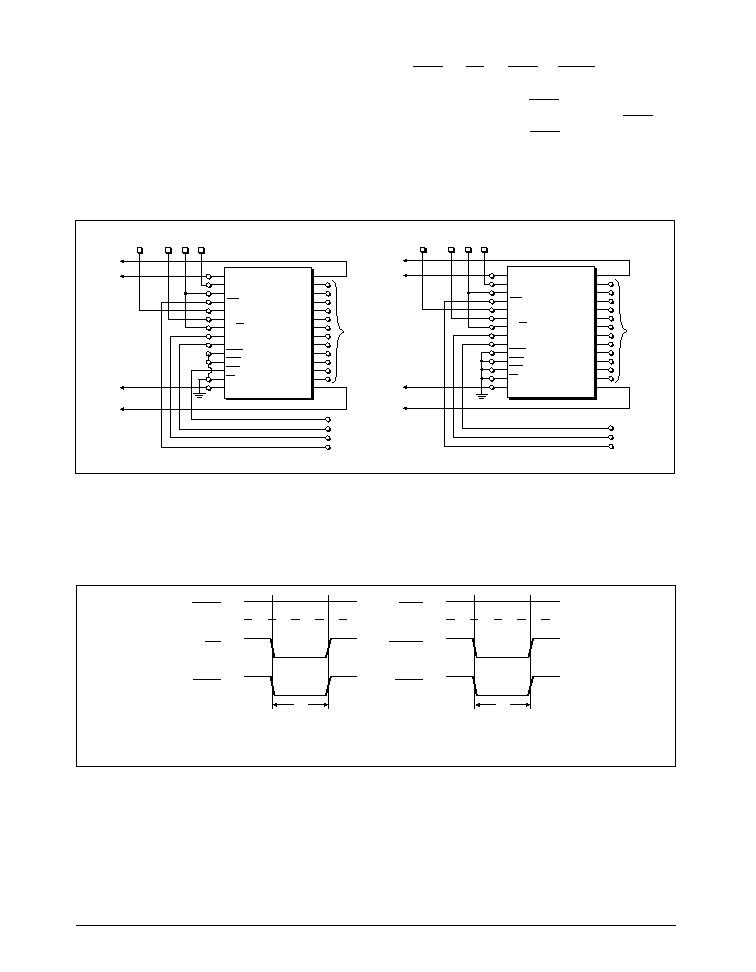
Figure 4. Timing
Figure 3. Latch Control Options -- (a) Semi≠Transparent Latch Mode; (b) Fully≠Transparent Latch Mode
on-reset. Using this feature, the SP9504 can be
configured such that during power-up, the
second register will be digitally "zeroed",
producing a zero volt output at each of the four
DAC outputs. This is achieved by powering the
unit up with XFER in a high state. Thus, with no
external circuitry, the SP9504 can be powered
up with the analog outputs at a known, zero volt
output level.
TEMPORARILY FORCING
ALL DAC OUTPUTS TO 0V
Set
WR1=1, CS=1, WR2=0, XFER=0. The DAC
registers can be temporarily forced to 1000 0000
0000 by bringing the CLR pin low. This will
force the DAC outputs to 0V, while the CLR pin
remains low. When the CLR pin is brought back
high, the digital code at the DAC registers will
again appear at the DAC's digital inputs, and the
analog outputs will return to their previous values.
1
2
3
4
5
6
7
8
9
10
11
12
13
14
28
27
26
25
24
23
22
21
20
19
18
17
16
15
V
OUT4
V
SS
V
DD
CLR
REF IN
GND
B1/B2
A
0
A
1
XFER
WR2
WR1
CS
V
OUT1
V
OUT3
DB
0
DB
1
DB
2
DB
3
DB
4
DB
5
DB
6
DB
7
DB
8
DB
9
DB
10
(MSB) DB
11
V
OUT2
SP9504
+5V ≠5V
12≠Bit
Data
Bus
V
OUT4
V
OUT3
V
OUT1
V
OUT2
+3V
Reference
GND
Address
Decode &
Control
DAC Strobe
1
2
3
4
5
6
7
8
9
10
11
12
13
14
28
27
26
25
24
23
22
21
20
19
18
17
16
15
V
OUT4
V
SS
V
DD
CLR
REF IN
GND
B1/B2
A
0
A
1
XFER
WR2
WR1
CS
V
OUT1
V
OUT3
DB
0
DB
1
DB
2
DB
3
DB
4
DB
5
DB
6
DB
7
DB
8
DB
9
DB
10
(MSB) DB
11
V
OUT2
SP9504
+5V ≠5V
12≠Bit
Data
Bus
V
OUT4
V
OUT3
V
OUT1
V
OUT2
+3V
Reference
GND
Address
Decode &
Control
(a)
(b)
H
L
H
L
H
L
CLR
XFER
WR2
140ns, t
H
L
H
L
H
L
WR2
CS
WR1
140ns, t
Data Transfer from
Input Register to DAC's
Loads Input Data to
First Set of Latches
WR
XFER
SP9504DS/03
SP9504 Quad, 12-Bit, Voltage Output D/A Converter
© Copyright 2000 Sipex Corporation
9
D
D1 = 0.005" min.
(0.127 min.)
E
PACKAGE: PLASTIC
DUAL≠IN≠LINE
(WIDE)
DIMENSIONS (Inches)
Minimum/Maximum
(mm)
A = 0.25" max.
(6.350 max).
E1
C
ÿ
L
A2
A1 = 0.015" min.
(0.381min.)
B
B1
e = 0.100 BSC
(2.540 BSC)
e
A
= 0.600 BSC
(15.240 BSC)
A2
B
B1
C
D
E
E1
L
ÿ
40≠PIN
0.125/0.195
(3.175/4.953)
0.014/0.022
(0.366/0.559)
0.030/0.070
(0.762/1.778)
0.008/0.015
(0.203/0.381)
1.980/2.095
(50.29/53.21)
0.600/0.625
(15.24/15.87)
0.485/0.580
(12.31/14.73)
0.115/0.200
(2.921/5.080)
0∞/ 15∞
(0∞/15∞)
48≠PIN
0.125/0.195
(3.175/4.953)
0.014/0.022
(0.366/0.559)
0.030/0.070
(0.762/1.778)
0.008/0.015
(0.203/0.381)
2.385/2.480
(60.57/62.99)
0.600/0.625
(15.24/15.87)
0.485/0.580
(12.31/14.73)
0.115/0.200
(2.921/5.080)
0∞/ 15∞
(0∞/15∞)
24≠PIN
0.125/0.195
(3.175/4.953)
0.014/0.022
(0.366/0.559
0.030/0.070
(0.762/1.778)
0.008/0.015
(0.203/0.381)
1.150/1.290
(29.21/32.76)
0.600/0.625
(15.24/15.87)
0.485/0.580
(12.31/14.73)
0.115/0.200
(2.921/5.080)
0∞/ 15∞
(0∞/15∞)
28≠PIN
0.125/0.195
(3.175/4.953)
0.014/0.022
(0.366/0.559
0.030/0.070
(0.762/1.778)
0.008/0.015
(0.203/0.381)
1.380/1.565
(35.05/39.75)
0.600/0.625
(15.24/15.87)
0.485/0.580
(12.31/14.73)
0.115/0.200
(2.921/5.080)
0∞/ 15∞
(0∞/15∞)
32≠PIN
0.125/0.195
(3.175/4.953)
0.014/0.022
(0.366/0.559
0.030/0.070
(0.762/1.778)
0.008/0.015
(0.203/0.381)
1.645/1.655
(41.78/42.04)
0.600/0.625
(15.24/15.87)
0.485/0.580
(12.31/14.73)
0.115/0.200
(2.921/5.080)
0∞/ 15∞
(0∞/15∞)
SP9504DS/03
SP9504 Quad, 12-Bit, Voltage Output D/A Converter
© Copyright 2000 Sipex Corporation
10
D
E
H
PACKAGE: PLASTIC
SMALL OUTLINE (SOIC)
DIMENSIONS (Inches)
Minimum/Maximum
(mm)
A
A1
ÿ
L
B
e
A
A1
B
D
E
e
H
L
ÿ
28≠PIN
0.090/0.100
(2.29/2.54)
0.004/0.010
(0.102/0.254)
0.014/0.020
(0.36/0.48)
0.706/0.718
(17.93/18.24)
0.340/0.350
(8.64/8.89)
0.050 BSC
(1.270 BSC)
0.463/0.477
(11.76/12.12)
0.020/0.042
(0.51/1.07)
0∞/8∞
(0∞/8∞)
SP9504DS/03
SP9504 Quad, 12-Bit, Voltage Output D/A Converter
© Copyright 2000 Sipex Corporation
11
ORDERING INFORMATION
Model
Temperature Range
Package
Monolithic 12-Bit Quad DAC Voltage Output:
SP9504JP .................................................................................. 0∞C to +70∞C ...................................................................... 28-pin, 0.6" Plastic DIP
SP9504KP ................................................................................. 0∞C to +70∞C ...................................................................... 28-pin, 0.6" Plastic DIP
SP9504JS .................................................................................. 0∞C to +70∞C ............................................................................. 28≠pin, 0.35" SOIC
SP9504KS ................................................................................. 0∞C to +70∞C ............................................................................. 28≠pin, 0.35" SOIC
Please consult the factory for pricing and availability on a Tape-On-Reel option.
Corporation
SIGNAL PROCESSING EXCELLENCE
Sipex Corporation reserves the right to make changes to any products described herein. Sipex does not assume any liability arising out of the
application or use of any product or circuit described hereing; neither does it convey any license under its patent rights nor the rights of others.
Sipex Corporation
Headquarters and
Sales Office
22 Linnell Circle
Billerica, MA 01821
TEL: (978) 667-8700
FAX: (978) 670-9001
e-mail: sales@sipex.com
Sales Office
233 South Hillview Drive
Milpitas, CA 95035
TEL: (408) 934-7500
FAX: (408) 935-7600