
1
Date: 8/25/04 SPX1117 800mA Low Dropout Voltage Regulator
© Copyright 2004 Sipex Corporation
800mA Low Dropout Voltage Regulator
SPX1117
DESCRIPTION
FEATURES
Guaranteed 0.8A Output Current
Guaranteed 1A Peak Current
Three Terminal Adjustable or Fixed
1.5V, 1.8V, 2.5V, 2.85V, 3.0V,
3.3V and 5V
Low Quiescent Current
Low Dropout Voltage of 1.1V at 0.8A
0.1% Line and 0.2% Load Regulation
Stable with 2.2uF Ceramic Capacitor
Overcurrent and Thermal Protection
Available Packages: SOT-223,TO-252,
TO-220, and TO-263
Æ
The SPX1117 is a low power positive-voltage regulator designed to satisfy moderate power
requirements with a cost effective, small footprint solution. This device is an excellent choice for
use in battery-powered applications and portable computers. The SPX1117 features very low
quiescent current and a low dropout voltage of 1.1V at a full load. As output current decreases,
quiescent current flows into the load, increasing efficiency. SPX1117 is available in adjustable
or fixed 1.5V, 1.8V, 2.5V,2.5V, 2.85V, 3.0V, 3.3V and 5V output voltages.
The SPX1117 is offered in several 3-pin surface mount packages: SOT-223, TO-252, TO-220
and TO-263. An output capacitor of 10µF provides unconditional stability while a smaller 2.2µF
capacitor is sufficient for most applications.
APPLICATIONS
Desktop PC's Servers
SCSI-II Active Terminator
Portable/ Palm Top / Notebook
Computers
Cordless Phones
Battery Chargers
Disk Drives
Portable Consumer Equipment
Portable Instrumentation
SMPS Post-Regulator
FUNCTIONAL DIAGRAM
Current Limit
I
CL
I
TL
Thermal Limit
V
REF
AMP
V
OUT
V
IN
ADJ/GND
+
≠
I
ADJ
~ 50µA
≠
1.25V
+
-
+
-
Now Available in Lead Free Packaging

2
Date: 8/25/04 SPX1117 800mA Low Dropout Voltage Regulator
© Copyright 2004 Sipex Corporation
ELECTRICAL CHARACTERISTICS
T
A
= 25
∞C, C
IN
= C
OUT
= 10
µF, unless otherwise specified. The Boldface applies over the full operating temperature range.
PARAMETER
CONDITIONS
MIN
TYP
MAX
UNITS
1.5V Version
Output Voltage
I
OUT
= 10mA, V
IN
=3.0V, T
J
= 25∫C
1.485
1.500
1.515
V
10mA
I
OUT
800mA, 2.9V V
IN
10V
1.470
1.530
1.8V Version
Output Voltage
I
OUT
= 10mA, V
IN
=3.3V, T
J
= 25∫C
1.782
1.800
1.818
V
10mA
I
OUT
800mA, 3.2V V
IN
10V
1.764
1.836
2.5V Version
Output Voltage
I
OUT
= 10mA, V
IN
=4.0V, T
J
= 25∫C
2.475
2.500
2.525
V
10mA
I
OUT
800mA, 3.9V V
IN
10V
2.450
2.550
2.85V Version
Output Voltage
I
OUT
= 10mA, V
IN
=4.35V, T
J
= 25∫C
2.821
2.850
2.878
V
10mA
I
OUT
800mA, 4.25V V
IN
10V
2.793
2.907
3.00V Version
Output Voltage
I
OUT
= 10mA, V
IN
=4.5V, T
J
= 25∫C
2.970
3.000
3.030
V
10mA
I
OUT
800mA, 4.4V V
IN
10V
2.940
3.060
3.30V Version
Output Voltage
I
OUT
= 10mA, V
IN
=4.8V, T
J
= 25∫C
3.267
3.300
3.333
V
10mA
I
OUT
800mA, 4.7V V
IN
10V
3.234
3.366
5V Version
Output Voltage I
OUT
= 10mA, V
IN
=6.5V
4.950
5
5.050
V
10mA
I
OUT
800mA, 6.4V V
IN
12V
4.90
5.10
All Voltage Options
Reference Voltage
I
OUT
=10mA, (V
IN
- V
OUT
)= 2V, T
J
= 25∫C
1.238
1.250
1.262
V
10mA
I
OUT
800mA, 1.4V(V
IN
-V
OUT
)
10V
1.225
1.270
Output Voltage
0.3
%
Temperature Stability
Line Regulation
V
INMIN
V
IN
12V,V
OUT
=Fixed/Adj,
(Note 1)
I
OUT
=10mA
3
7
mV
Load Regulation
10mA
I
OUT
800mA,V
OUT
=Fixed/Adj
6
12
mV
(Note 1)
Dropout Voltage
I
OUT
=100mA
1.00
1.10
V
(Note 2)
I
OUT
=500mA
1.05
1.15
I
OUT
=800mA
1.10
1.20
Quiescent Current
4.25V
V
IN
6.5V
5
10
mA
Power Dissipation.......................................Internally Limited
Lead Temperature (soldering, 5 seconds) ...............260∞C
Storage Temperature Range.......................-65∞C to +150∞C
Operating Junction Temperature Range.....-40∞C to +125∞C
Input Supply Voltage .................................................... +20V
Input to Output Voltage ................................................ 18.8V
ESD Rating.................................................................2kV min
These are sterss ratings only and functional operation of the
device at these ratings or any other above those indicated in the
operation sections of the specifications below is not implied.
Exposure to absolute maximum rating conditions for extended
periods of time may affect reliability.
ABSOLUTE MAXIMUM RATINGS

3
Date: 8/25/04 SPX1117 800mA Low Dropout Voltage Regulator
© Copyright 2004 Sipex Corporation
ELECTRICAL CHARACTERISTICS
T
A
= 25
∞C, C
IN
= C
OUT
= 10
µF, unless otherwise specified. The Boldface applies over the full operating temperature range.
PARAMETER
CONDITIONS
MIN
TYP
MAX
UNITS
Adjust Pin Current
50
120
µA
Current Limit
(V
IN
-V
OUT
)=5V
1.0
1.5
2.0
A
Thermal Regulation
25
∞C, 30mS pulse
0.01
0.1
%/W
Ripple Rejection
f
RIPPLE
=120Hz, (V
IN
-V
OUT
)=2V,
60
75
dB
V
RIPPLE
=1V
PP
Long Term Stability
125
∞C, 1000Hrs
0.03
%
RMS Output Noise
% of V
OUT
, 10Hz
f10kHz
0.003
%
Thermal Resistance
TO-220 Junction to Case, at Tab
3
∞C/W
TO-220 Junction to Ambient
60
TO-263 Junction to Case, at Tab
3
TO-263 Junction to Ambient
60
TO-252 Junction to Case, at Tab
6
TO-252 Junction to Ambient
126
SOT-223 Junction to Case, at Tab
15
SOT-223 Junction to Ambient
156
*Note 1 - For fixed option, V
INMIN
= V
OUT
+ 1.5V
- For adjustable option, V
INMIN
= V
IN
- V
OUT
= 1.4V
*Note 2 - Dropout voltage is the input voltage minus output voltage that produces a 1% decrease in output voltage with respect
to the nominal output voltage at V
IN
= V
OUT
+ 1.5V

4
Date: 8/25/04 SPX1117 800mA Low Dropout Voltage Regulator
© Copyright 2004 Sipex Corporation
TYPICAL PERFORMANCE CHARACTERISTICS
Figure 1. Load Regulation for SPX1117M3-3.3;
Figure 2. Line Regulation for SPX1117M3-3.3;
V
IN
=4.8V
I
OUT
=10mA
Figure 3. Dropout Voltage vs Output Current for
SPX1117M3-3.3; V
IN
=4.8V, C
OUT
=2.2
µF
Figure 5. Current Limit for SPX1117M3-3.3, Output
Voltage Deviation with I
OUT
=10mA to 1A Step
3.280
3.285
3.290
3.295
3.300
3.305
3.310
3.315
3.320
10
100
1000
Output Current (mA)
Output V
oltage
3.300
3.305
3.310
3.315
3.320
3.325
4.5
6.5
8.5
10.5
12.5
14.5
Vin (V)
V
out (V)
0.9
1.0
1.1
1.2
1.3
100
200
300
400
500
600
700
800
900
1000
Io (mA)
Dropout V
oltage (V)
1.225
1.23
1.235
1.24
1.245
1.25
1.255
1.26
1.265
1.27
1.275
-50
-30
-10
10
30
50
70
90
110
130
Temp (C)
V
out (V)
1.25v Adj
125∞C
22µF
Indicating Current
Limit Starts
V
IN
= 4.0V
V
IN
=3.3V Fixed
1
O
=10mA
C
IN
=1µF Tan Cap
C
OUT
=2.2µF Tan Cap
100
0
-100
1.5
1.0
0.5
0
0
0.1
0.2
0.3
0.4
0.5
0.6
0.7
0.8
0.9
1.0
Time (ms)
Output Current
(A)
Output Deviation
(mV)
0.00
0.50
1.00
1.50
2.00
-50
-25
0
25
50
75
100
125
Temp (
o
C)
Current Limit (A)
Figure 6. V
OUT
vs Temperature, V
IN
=2.5V, I
OUT
=10mA
Figure 4. Current Limit for SP1117M3-3.3; V
IN
=4.8V,
C
IN
=C
OUT
=1
µF, I
OUT
pulsed from 10mA to Current
Limit

5
Date: 8/25/04 SPX1117 800mA Low Dropout Voltage Regulator
© Copyright 2004 Sipex Corporation
Figure 7. V
IN
=3.0V, I
OUT
=10mA
Figure 9. V
IN
=4.0V, I
OUT
=10mA
Figure 12. V
IN
=5.0V, I
OUT
=10mA
TYPICAL PERFORMANCE CHARACTERISTICS: Continued
1.47
1.48
1.49
1.5
1.51
1.52
1.53
-50
-30
-10
10
30
50
70
90
110
130
Temp (C)
V
out (V)
1.5v Adj
1.5v Fixed
1.76
1.77
1.78
1.79
1.8
1.81
1.82
1.83
1.84
-50
-30
-10
10
30
50
70
90
110
130
Temp (C)
V
out (V)
1.8v Adj
1.8v Fixed
2.45
2.46
2.47
2.48
2.49
2.5
2.51
2.52
2.53
2.54
2.55
-50
-30
-10
10
30
50
70
90
110
130
Temp (C)
V
out (V)
2.5v Adj
2.5v Fixed
2.8
2.82
2.84
2.86
2.88
2.9
2.92
-50
-30
-10
10
30
50
70
90
110
130
Temp (C)
V
out (V)
2.85v Adj
2.85v Fixed
2.94
2.96
2.98
3
3.02
3.04
3.06
-50
-30
-10
10
30
50
70
90
110
130
Temp (C)
V
out (V)
3v Adj
3v Fixed
3.26
3.28
3.3
3.32
3.34
3.36
3.38
-50
-30
-10
10
30
50
70
90
110
130
Temp (C)
V
out (V)
3.3v Adj
3.3v Fixed
Figure 8. V
IN
=3.3V, I
OUT
=10mA
Figure 10. V
IN
=4.85V, I
OUT
=10mA
Figure 11. V
IN
=4.85V, I
OUT
=10mA
Figure 14. Output Voltage vs Temperature at different
Current Loads, V
IN
=3.3V, V
OUT
= 1.8V Adjustable
Figure 13. Line Regulation vs Temperature. V
OUT
=1.8V
(adjustable), V
IN
= 3.3V
-8
-6
-4
-2
0
2
4
6
-40
-20
0
20
40
60
80
100
Ambient Temperature,*C
Output V
oltage Change, mV
1.806
1.807
1.808
1.809
1.81
1.811
1.812
1.813
1.814
1.815
1.816
-40
-20
0
20
40
60
80
100
Ambient Temperature, *C
V out, V
800mA
400mA
10mA
Figure 15. Line Regulation at I
LOAD
=800mA over
Temperature, V
OUT
=1.8V adjustable
-0.3
-0.2
-0.1
0
0.1
0.2
0.3
0.4
3
4
5
6
Vin, V
V
out tolerance,%
-40∞C
+25∞C
+85∞C
6
Date: 8/25/04 SPX1117 800mA Low Dropout Voltage Regulator
© Copyright 2004 Sipex Corporation
Output Capacitor
To ensure the stability of the SPX1117, an
output capacitor of at least 2.2
µF (tantalum or
ceramic) or 10
µF (aluminum) is required. The
value may change based on the application
requirements of the output load or temperature
range. The value of ESR can vary based on the
type of capacitor used in the applications to
guarantee stability. The recommended value
for ESR is 0.5
or less. A larger value of
output capacitance (up to 100
µF) can improve
the load transient response.
Soldering Methods
The SPX1117 SOT-223 package is designed
to be compatible with infrared reflow or
vapor-phase reflow soldering techniques.
During soldering, the non-active or mildly
active fluxes may be used. The SPX1117 die
is attached to the heatsink lead which exits
opposite the input, output, and ground pins.
Hand soldering and wave soldering should be
avoided since these methods can cause
damage to the device with excessive thermal
gradients on the package. The SOT-223
recommended soldering method are as
follows: vapor phase reflow and infrared
reflow with the component preheated to within
65
∞C of the soldering temperature range.
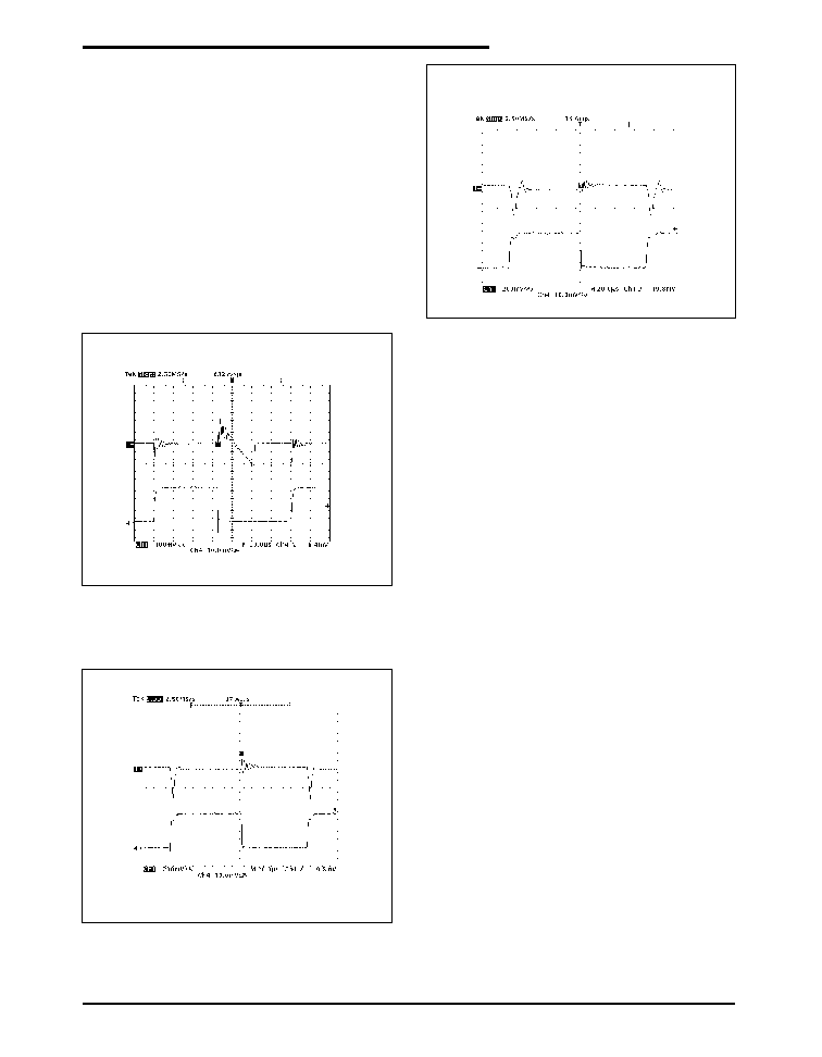
Figure 16. Load Step Response (0 to 800mA), Vin=3.3V,
Vout=1.8V, Cin=10
µF, Cout=2.2µF, Ceramic; 1 = Vout,
4= Iload
Figure 17. Load Step Response (0 to 800mA), Vin=3.3V,
Vout=1.8V, Cin=10
µF, Cout=2.2µF, OSCON; 1 = Vout,
4= Iload
APPLICATION INFORMATION

7
Date: 8/25/04 SPX1117 800mA Low Dropout Voltage Regulator
© Copyright 2004 Sipex Corporation
Thermal Characteristics
The thermal resistance of SPX1117 (SOT-223
Package) is 15
∞C/W from junction to tab and 31
∞C/W from tab to ambient for a total of 46 ∞C/W
from junction to ambient (Table 1). The SPX1117
features the internal thermal limiting to protect
the device during overload conditions. Special
care needs to be taken during continuous load
conditions such that the maximum junction tem-
perature does not exceed 125
∞C. Thermal pro-
tection is activated at >155
∞C and deactiviated
at <140
∞C.
Taking the FR-4 printed circuit board and 1/16
thick with 1 ounce copper foil as an experiment
(fig.13), the PCB material is effective at trans-
mitting heat with the tab attached to the pad area
and a ground plane layer on the backside of the
substrate. Refer to table 1 for the results of the
experiment.
The thermal interaction from other components
in the application can effect the thermal resis-
tance of the SPX1117. The actual thermal
resistance can be determined with experimenta-
tion.
SPX1117 power dissipation is calculated as
follows:
P
D
= (V
IN
- V
OUT
)(I
OUT
)
Maximum Junction Temperature range:
T
J
= T
A
(max) + P
D
* thermal resistance
(junction-to-ambient)
Maximum junction temperature must not ex-
ceed the 125
∞C.
Ripple Rejection
Ripple rejection can be improved by adding a
capacitor between the ADJ pin and ground as
shown in Figure 23. When ADJ pin bypassing
is used, the value of the output capacitor re-
quired increases to its maximum. If the ADJ pin
is not bypassed, the value of the output capacitor
can be lowered to 10
µF for an electrolytic alu-
minum capacitor or 2.2
µF for a ceramic or solid
tantalum capacitor (Fig 22).
However the value of the ADJ-bypass capacitor
should be chosen with respect to the following
equation:
C = 1 / ( 6.28 * F
R
* R
1
)
Where
C = value of the capacitor in Farads
(select an equal or larger standard value),
F
R
= ripple frequency in Hz,
R
1
= value of resistor R1 in Ohms.
If an ADJ-bypass capacitor is used, the ampli-
tude of the output ripple will be independent of
the output voltage. If an ADJ-bypass capacitor
is not used, the output ripple will be proportional
to the ratio of the output voltage to the reference
voltage:
M = V
OUT
/ V
REF
Where M = multiplier for the ripple seen when
the ADJ pin is optimally bypassed.
V
REF
=1.25V
Ripple rejection for the adjustable version is
shown in Figure 20.
Figure 19. Substrate Layout for SOT-223
50 X 50mm
35 X 17mm
16 X 10mm
-90
-80
-70
-60
-50
-40
-30
-20
-10
0
10
100
1000
10000
100000
1000000
Frequency, Hz
Ripple Rejection, Db
Figure 20. Ripple Rejection; Vin=3.3V, Vout=1.8V
(adj.), Iload=200mA
APPLICATION INFORMATION: Continued

8
Date: 8/25/04 SPX1117 800mA Low Dropout Voltage Regulator
© Copyright 2004 Sipex Corporation
Output Voltage
The output of the adjustable regulator can be set
to any voltage between 1.25V and 15V. The
value of V
OUT
can be quickly approximated using
the formula
V
OUT
=1.25 *(R
1
+ R
2
)/R
1
.
A small correction to this formula is required
depending on the values of resistors R
1
and R
2
,
since the adjustable pin current (approx 50
µA)
flows through R
2
. When I
ADJ
is taken into ac-
count, the formula becomes
PC BOARD TOPSIDE COPPER BACKSIDE COPPER
THERMAL RESISTANCE
JUNC. TO AMB.
mm
2
mm
2
mm
2
∞C/W
2500
2500
2500
46
2500
1250
2500
47
2500
950
2500
49
2500
2500
0
51
2500
1800
0
53
1600
600
1600
55
2500
1250
0
58
2500
915
0
59
1600
600
0
67
900
240
900
72
900
240
0
85
V
OUT
= V
REF
(1+ (R
2
/R
1
)) + I
ADJ
* R
2
,
where
V
REF
=1.25V.
Layout Considerations
Parasitic line resistance can degrade load regu-
lation. In order to avoid this, connect R
1
directly
to V
OUT
as illustrated in Figure 25. For the same
reason, R
2
should be connected to the negative
side of the load.
Figure 21. Current Source
Figure 22. Typical Adjustable Regulator
LOAD
ADJ
SPX1117
V
IN
C
1
OUT
IN
4.7µF
C
2
I
OUT
R
1
V
REF
R
1
I
OUT
=
+
V
OUT
IN
OUT
I
ADJ
SPX1117
C
1
R
1
R
2
V
OUT
V
IN
C
2
V
OUT
= V
REF
(1+R
2
/R
1
) +I
ADJ
R
2
V
REF
50µA
ADJ
4.7µF +
TABLE 1
APPLICATION INFORMATION: Continued

9
Date: 8/25/04 SPX1117 800mA Low Dropout Voltage Regulator
© Copyright 2004 Sipex Corporation
Figure 24. 5V Regulator with Shutdown
SPX1117
V
IN
R
1
R
2
10µF
10µF*
1k,
330
1%
+
+
4.7µF
C
1
*C
1
improves ripple rejection.
Z
C
should be ~ R1 at ripple frequency
5V
ADJ
IN
OUT
(Note A)
V
OUT
Note A: V
IN(MIN)
= (Intended V
OUT
) + (V
DROPOUT (MAX)
)
1%
1k
SPX1117
10µF
1%
330W
1%
+
+
4.7µF
5V
ADJ
IN
OUT
(Note A)
1K
1k
TTL
Input
2N3904
DROPOUT (MAX)
Note A: V
IN(MIN)
= (Intended V
OUT
) + (V
)
V
IN
Figure 25. Recommended Connections for Best Results
Figure 23. Improving Ripple Rejection
SPX1117
R
2
R
1
Connect R
2
to Load
R
L
Connect R to
Case of Regulator
R
P
Parasitic Line
Resistance
ADJ
V
OUT
V
IN
APPLICATION INFORMATION: Continued
PINOUTS
1
3
2
SOT-223 (M3)
Top View
TO-263-3 (T)
1
2
3
Front View
TO-220-3 (U)
1
2
3
Front View
TO-252 (R)
ADJ/GND
V
OUT
1
2
3
V
IN
ADJ/GND
V
OUT
V
IN
ADJ/GND
V
OUT
V
IN
ADJ/GND
V
OUT
V
IN
Top View
10
Date: 8/25/04 SPX1117 800mA Low Dropout Voltage Regulator
© Copyright 2004 Sipex Corporation
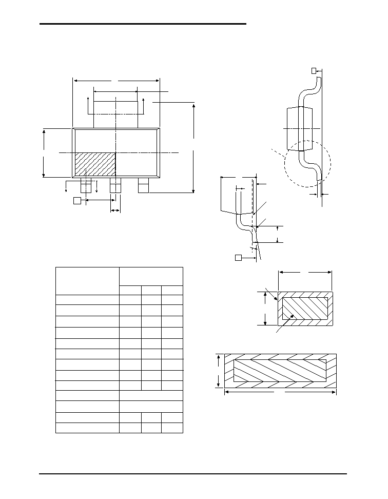
PACKAGE: 3 PIN SOT-223
See detail
A
C
b2
c
GAUGE
PLANE
SEATING
PLANE
H
A
A1
L
C
0
E
D
1
e
E1
C
C
N
B
B
b2
b
Section C-C
- - 1.80
0.02 - 0.10
Dimensions in (mm)
3 PIN SOT-223
JEDEC TO-261
(AA) Variation
6.50
6.70 7.00 7.30
A
A1
D
E
E1
e
L
MIN NOM MAX
c
0.23
0.30
0.35
6.30
6.70
¯
0∫
-
10∫
A2
1.50 1.60 1.70
0.66 0.76 0.84
b
b2
2.90 3.00 3.10
3.30 3.50 3.70
2.30 BASIC
e1
4.60 BASIC
0.75 - -
c
WITH PLATING
BASE METAL
b
Section B-B
3 PIN SOT-223

11
Date: 8/25/04 SPX1117 800mA Low Dropout Voltage Regulator
© Copyright 2004 Sipex Corporation
PACKAGE: 3 PIN TO-252
4
3
2
1
E
b
2
-A-
L
2
D
L
3
L
1
b
1
e
-C-
e1
D
1
E
1
BACK VIEW A-A
TERM 4
C
.010
M
A M
3 PLCS
-B-
A
A
1
C
1
c
8
A
A
SEATING
PLANE
H
L
NOTES
1. Refer To Applicable Symbol List.
2. Dimensions And Tolerancing Per Ansi Y14.5m - 1982.
3. Lead Dimension Uncontrolled in L3
4. Tab Contour Optional Within Dim. b2 & L2 And E1 & D1
5. D1 & E1 Establishes A Minimum Mounting Surface for
Terminal 4.
6. L is the Termal Length for Soldering.
7. Controlling Dimension: Inch
8. 2 Mils Suggested For Postive Contact At Mounting.
S
Y
M
B
O
L
MIN.
N
O
T
E
INCHES
MAX
MIN.
MAX
0.098
0.180
2.184
0.889
0.635
7.620
5.207
0.457
0.457
5.969
4.318
6.350
4.318
9.398
0.508
0.635
0.889
1.143
4
4,5
4,5
6
4
3
MM
2.3876
1.143
0.889
1.143
5.461
0.5842
0.5842
6.223
-
6.731
-
10.414
-
1.016
1.270
1.524
A
A1
b
b1
b2
c
c1
D
D1
E
E1
e
e1
H
L
L1
L2
L3
0.086
0.035
0.025
0.300
0.205
0.018
0.018
0.235
0.170
0.250
0.170
0.370
0.020
0.025
0.035
0.045
0.094
0.045
0.035
0.045
0.215
0.023
0.023
0.245
-
0.265
-
0.410
-
0.040
0.050
0.060
2.489
4.572

12
Date: 8/25/04 SPX1117 800mA Low Dropout Voltage Regulator
© Copyright 2004 Sipex Corporation
PACKAGE: 3 PIN TO-220
H1
B
SEATING
PLANE
A1
A
CHAMFER
OPTIONAL
C
A2
A
A
.140 - .190
.020 - .055
Dimensions in
(mm)
3 PIN TO-220
JEDEC TO-220
(AB) Variation
.080 - .115
.015 .027 .040
.015 - .038
.045 - .070
.014 - .022
.480 - .507
A
A1
A2
b
b1
b2
b3
c1
D1
D2
.380 - .420
E
MIN NOM MAX
.045 - .068
c
.014 - .024
D
.560 - .650
.330 - .355
E1
.270
-
.350
E2
- - .030
e
.100 BSC
e1
.200 BSC
N
4
H1
.230 - .270
L1
- - .250
L2
- - -
P
.139 - .161
Q
.100 -
.135
E
¯P
Q
D
D1
E2
E/2
L
L1
C
C
D
D
2X
3X b

13
Date: 8/25/04 SPX1117 800mA Low Dropout Voltage Regulator
© Copyright 2004 Sipex Corporation
PACKAGE: 3 PIN TO-263
0.103 BSC
0.356
0.005
(9.042
0.127)
±
±
(15.24 0.635)
±
(2.616)
0.032
+-
0.001
(0.813
0.025)
+-
0.176 0.005
0.050 0.002
0.015
+-
0.003
0∞ 8∞
(0.381
0.074)
+
-
0.100
0.010
(2.540
0.254)
±
±
(4.470
0.127)
±
(1.270
0.051)
±
±
±
0.050 (1.270)
0.405 ± 0.005
(10.287 ± 0.127)
0.055 (1.397)
0.600 ± 0.025
14
Date: 8/25/04 SPX1117 800mA Low Dropout Voltage Regulator
© Copyright 2004 Sipex Corporation
Corporation
ANALOG EXCELLENCE
Sipex Corporation reserves the right to make changes to any products described herein. Sipex does not assume any liability arising out of the
application or use of any product or circuit described herein; neither does it convey any license under its patent rights nor the rights of others.
Headquarters and
Sales Office
233 South Hillview Drive
Milpitas, CA 95035
TEL: (408) 934-7500
FAX: (408) 935-7600
ORDERING INFORMATION
PART NUMBER ACC. OUTPUT VOLTAGE
PACKAGE
SPX1117M3 ................................. 1% ...................................... Adj .......................... 3 Pin SOT-223
SPX1117M3/TR ........................... 1% ...................................... Adj .......................... 3 Pin SOT-223
SPX1117M3-1.5 ........................... 1% ..................................... 1.5V ......................... 3 Pin SOT-223
SPX1117M3-1.5/TR ..................... 1% ..................................... 1.5V ......................... 3 Pin SOT-223
SPX1117M3-1.8 ........................... 1% ..................................... 1.8V ......................... 3 Pin SOT-223
SPX1117M3-1.8/TR ..................... 1% ..................................... 1.8V ......................... 3 Pin SOT-223
SPX1117M3-2.5 ........................... 1% ..................................... 2.5V ......................... 3 Pin SOT-223
SPX1117M3-2.5/TR ..................... 1% ..................................... 2.5V ......................... 3 Pin SOT-223
SPX1117M3-2.85 ......................... 1% .................................... 2.85V ........................ 3 Pin SOT-223
SPX1117M3-2.85/TR ................... 1% .................................... 2.85V ........................ 3 Pin SOT-223
SPX1117M3-3.0 ........................... 1% ..................................... 3.0V ......................... 3 Pin SOT-223
SPX1117M3-3.0/TR ..................... 1% ..................................... 3.0V ......................... 3 Pin SOT-223
SPX1117M3-3.3 ........................... 1% ..................................... 3.3V ......................... 3 Pin SOT-223
SPX1117M3-3.3/TR ..................... 1% ..................................... 3.3V ......................... 3 Pin SOT-223
SPX1117M3-5.0 ........................... 1% ..................................... 5.0V ......................... 3 Pin SOT-223
SPX1117M3-5.0/TR ..................... 1% ..................................... 5.0V ......................... 3 Pin SOT-223
SPX1117R ................................... 1% ...................................... Adj ............................. 3 Pin TO-252
SPX1117R/TR ............................. 1% ...................................... Adj ............................. 3 Pin TO-252
SPX1117R-1.5 ............................. 1% ..................................... 1.5V ............................ 3 Pin TO-252
SPX1117R-1.5/TR ....................... 1% ..................................... 1.5V ............................ 3 Pin TO-252
SPX1117R-1.8 ............................. 1% ..................................... 1.8V ............................ 3 Pin TO-252
SPX1117R-1.8/TR ....................... 1% ..................................... 1.8V ............................ 3 Pin TO-252
SPX1117R-2.5 ............................. 1% ..................................... 2.5V ............................ 3 Pin TO-252
SPX1117R-2.5/TR ....................... 1% ..................................... 2.5V ............................ 3 Pin TO-252
SPX1117R-2.85 ........................... 1% .................................... 2.85V ........................... 3 Pin TO-252
SPX1117R-2.85/TR ..................... 1% .................................... 2.85V ........................... 3 Pin TO-252
SPX1117R-3.0 ............................. 1% ..................................... 3.0V ............................ 3 Pin TO-252
SPX1117R-3.0/TR ....................... 1% ..................................... 3.0V ............................ 3 Pin TO-252
SPX1117R-3.3 ............................. 1% ..................................... 3.3V ............................ 3 Pin TO-252
SPX1117R-3.3/TR ....................... 1% ..................................... 3.3V ............................ 3 Pin TO-252
/TR = Tape and Reel
Pack quantity is 500 for TO-263, 2,000 for TO-252, and 2,500 for SOT223.
Available in lead free packaging. To order add "-L" suffix to part number.
Example: SPX1117M3-5.0/TR = standard; SPX1117M3-L-5.0/TR = lead free

15
Date: 8/25/04 SPX1117 800mA Low Dropout Voltage Regulator
© Copyright 2004 Sipex Corporation
PART NUMBER ACC. OUTPUT VOLTAGE
PACKAGE
SPX1117T .................................... 1% ...................................... Adj ............................. 3 Pin TO-263
SPX1117T/TR .............................. 1% ...................................... Adj ............................. 3 Pin TO-263
SPX1117T-1.5 ............................. 1% ..................................... 1.5V ............................ 3 Pin TO-263
SPX1117T-1.5/TR ........................ 1% ..................................... 1.5V ............................ 3 Pin TO-263
SPX1117T-1.8 ............................. 1% ..................................... 1.8V ............................ 3 Pin TO-263
SPX1117T-1.8/TR ........................ 1% ..................................... 1.8V ............................ 3 Pin TO-263
SPX1117T-2.5 ............................. 1% ..................................... 2.5V ............................ 3 Pin TO-263
SPX1117T-2.5/TR ........................ 1% ..................................... 2.5V ............................ 3 Pin TO-263
SPX1117T-2.85 ........................... 1% .................................... 2.85V ........................... 3 Pin TO-263
SPX1117T-2.85/TR ...................... 1% .................................... 2.85V ........................... 3 Pin TO-263
SPX1117T-3.0 ............................. 1% ..................................... 3.0V ............................ 3 Pin TO-263
SPX1117T-3.0/TR ........................ 1% ..................................... 3.0V ............................ 3 Pin TO-263
SPX1117T-3.3 ............................. 1% ..................................... 3.3V ............................ 3 Pin TO-263
SPX1117T-3.3/TR ........................ 1% ..................................... 3.3V ............................ 3 Pin TO-263
SPX1117U ................................... 1% ...................................... Adj .............................. 3 Pin TO220
SPX1117U-1.5 ............................. 1% ..................................... 1.5V ............................. 3 Pin TO220
SPX1117U-1.8 ............................. 1% ..................................... 1.8V ............................. 3 Pin TO220
SPX1117U-2.5 ............................. 1% ..................................... 2.5V ............................. 3 Pin TO220
SPX1117U-2.85 ........................... 1% .................................... 2.85V ............................ 3 Pin TO220
SPX1117U-3.0 ............................. 1% ..................................... 3.0V ............................. 3 Pin TO220
SPX1117U-3.3 ............................. 1% ..................................... 3.3V ............................. 3 Pin TO220
ORDERING INFORMATION
Corporation
Sipex Corporation
Headquarters and
Sales Office
233 South Hillview Drive
Milpitas, CA 95035
TEL: (408) 934-7500
FAX: (408) 935-7600
Available in lead free packaging. To order add "-L" suffix to part number.
Example: SPX1117M3-5.0/TR = standard; SPX1117M3-L-5.0/TR = lead free
/TR = Tape and Reel
Pack quantity is 500 for TO-263, 2,000 for TO-252, and 2,500 for SOT223.