1
Date:5/25/04
SP29150/51/52/53 1.5A Low Dropout Voltage Regulator
© Copyright 2004 Sipex Corporation
1.5A Low Dropout Voltage Regulator
Adjustable & Fixed Output, Fast Response Time
SPX29150/51/52/53
DESCRIPTION
FEATURES
Adjustable Output Down To 1.25V
1% Output Accuracy
Output Current of 1.5A
Low Dropout Voltage of 390mV @
1.5A
Extremely Tight Load and Line
Regulation
Extremely Fast Transient Response
Reverse-Battery Protection
Zero Current Shutdown (5 pin version)
Error Flag Signal Output for Out of
Regulation State (5 pin version)
Standard TO-220 and TO-263
Packages
Æ
The SPX29150/51/52/53 are 1.5A, highly accuracy voltage regulators with a low drop out
voltage of 390mV dropout (typical) @ 1.5A. These regulators are specifically designed for low
voltage applications that require a low dropout voltage and a fast transient response. They
are fully fault protected against over-current, reverse battery, and positive and negative
voltage transients. On-Chip trimming adjusts the reference voltage to 1% initial accuracy.
Other features in the 5 pin versions include Enable, and Error Flag.
The SPX29150/51/52/53 is offered in 3 & 5-pin TO-220 & TO-263 packages. For a 3A version,
refer to the SPX29300 data sheet.
APPLICATIONS
Powering VGA & Sound Card
LCD Monitors
USB Power Supply
Power PCTM Supplies
SMPS Post Regulator
High Efficiency "Green" Computer
Systems
High Efficiency Linear Power Supplies
Portable Instrumentation
Constant Current Regulators
Adjustable Power Supplies
Battery Charger
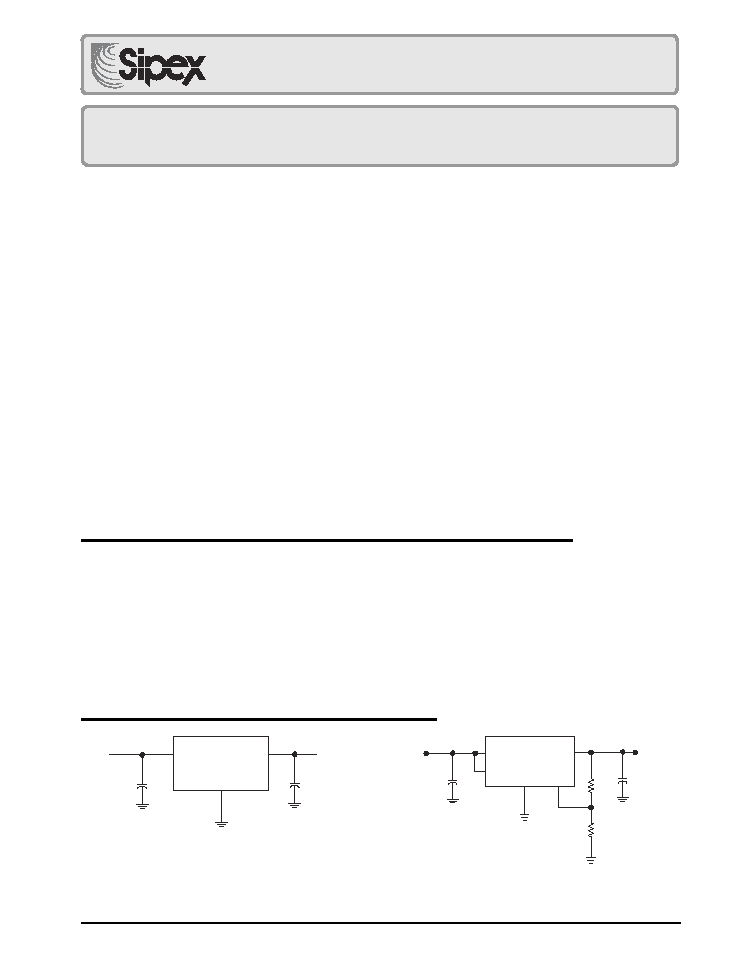
SPX29150
V
OUT
V
IN
6.8 F
+
+ 10 F
1
2
3
SPX29152
VOUT
VIN
GND
ADJ
1
2
3
4
5
R1
R2
6.8 F
+
+ 10 F
Figure 1. Fixed Output Linear Regulator
Figure 2. Adjustable Output Linear Regulator
TYPICAL APPLICATION CIRCUIT
Now Available in Lead Free Packaging
Refer to page 8 for pinouts.

Date:5/25/04
SP29150/51/52/53 1.5A Low Dropout Voltage Regulator
© Copyright 2004 Sipex Corporation
2
ABSOLUTE MAXIMUM RATINGS
Lead Temperature (soldering, 5 seconds) ................260
∞
C
Storage Temperature Range........................-65
∞
C to +150
∞
C
Operating Junction Temperature Range......-40
∞
C to +125
∞
C
Input Voltage (Note 7) .................................................... 16V
at V
IN
=V
OUT
+ 1V and I
OUT
= 10mA, C
IN
= 6.8
µF, C
OUT
= 10
µF, T
A
= 25
∞C, unless otherwise specified. The Boldface applies
over the junction temperature range. Adjustable versions are set to 5.0V.
SPX29150/51
PARAMETER
CONDITIONS
TYP
MIN
MAX
UNITS
Fixed Voltage Options
1.8V Version
Output Voltage
I
OUT
= 10mA
1.8
1.782
1.818
V
10mA
I
OUT
1.5A, 2.5V V
IN
16V
1.8
1.764
1.836
2.5V Version
Output Voltage
I
OUT
= 10mA
2.5
2.475
2.525
V
10mA
I
OUT
1.5A, 3.5V V
IN
16V
2.5
2.450
2.550
3.3V Version
Output Voltage
I
OUT
= 10mA
3.3
3.267
3.333
V
10mA
I
OUT
1.5A, 4.3V V
IN
16V
3.3
3.234
3.366
5.0V Version
Output Voltage
I
OUT
= 10mA
5.0
4.950
5.050
V
10mA
I
OUT
1.5A, 6.0V V
IN
16V
5.0
4.900
5.100
All Voltage Options
SPX29150/51/52/53
Line Regulation
I
OUT
=10mA,(V
OUT
+1V)
V
IN
16V
0.1
0.5
%
Load Regulation
V
IN
=V
OUT
+1V, 10mA
I
OUT
I
FULLLOAD
0.2
1
%
V/T
V
OUT
Temp Coefficient
13
100
ppm/
∞C
Dropout Voltage
I
OUT
=100mA
70
200
mV
(Note 1, except 1.8V)
I
OUT
=750mA
230
I
OUT
=1.5A
390
600
Ground Current
I
OUT
=750mA, V
IN
=V
OUT
+1V
12
25
mA
(Note 3)
I
OUT
=1.5A
45
Ground Pin Current
V
IN
=0.1V less than specified V
OUT,
0.9
mA
at Dropout
I
OUT
=10mA
Current Limit
V
OUT
=0V (Note 2)
2.2
1.7
A
Output Noise Voltage
C
L
=10
µF
400
µV
RMS
(10Hz to 100kHz)
I
L
=100mA
C
L
=33
µF
260
Reference Voltage
Adjustable version only
1.240
1.228
1.252
V
1.215
1.265
Reference Voltage
Adjustable version only (Note 8)
1.203
1.277
Adjust Pin Bias Current
40
80
nA
120
Reference Voltage
(Note 4)
13
ppm/
∞C
Temp. Coeff.
Adjust Pin Bias
0.1
nA/
∞C
Current Temp. Coeff.
ELECTRICAL CHARACTERISTICS
3
Date:5/25/04
SP29150/51/52/53 1.5A Low Dropout Voltage Regulator
© Copyright 2004 Sipex Corporation
at V
IN
=V
OUT
+ 1V and I
OUT
= 10mA, C
IN
= 6.8
µF, C
OUT
= 10
µF, T
A
= 25
∞C, unless otherwise specified. The Boldface applies
over the junction temperature range. Adjustable versions are set to 5.0V.
PARAMETER
CONDITIONS
TYP
MIN
MAX
UNITS
FLAG OUTPUT (ERROR COMPARATOR)
SPX29150/29151/29153
Output Leakage
V
OH
=16V
0.1
1
µA
Current
2
Output Low Voltage
Device set for 5V,V
IN
=4.5V, I
OL
=250
µA
200
300
mV
400
Upper Threshold
Device set for 5V, (Note 5)
60
40
mV
Voltage
25
Lower Threshold
Device set for 5V, (Note 5)
75
95
mV
Voltage
140
Hysteresis
Device set for 5V, (Note 5)
15
mV
ENABLE Input
SPX29151/29152
Input Logic Voltage
Low (OFF)
V
IN
<10V
0.8
V
High (ON)
2.4
ENABLE Input Pin
V
EN
=16V
100
600
µA
750
V
EN
=0.8V
1
µA
2
Regulator Output
(Note 6)
10
500
µA
Current in Shutdown
Thermal Resistance
TO-200 Junction to Case, at Tab
3
∞C/W
TO-220 Junction to Ambient
60
TO-263Junction to Case, at Tab
3
TO-263 Junction to Ambient
60
NOTES:
Note 1: Dropout voltage is defined as the input to output differential when the output voltage drops to 99% of its nominal value.
Note 2: V
IN
= V
OUT
(NOMINAL) +1V. For example, use V
IN
= 4.3V for a 3.3V regulator. Employ pulse-testing procedures to minimize temperature rise.
Note 3: Ground pin current is the regulator quiescent current. The total current drawn from the source is the sum of the load current to the ground current.
Note 4: Thermal regulation is defined as the change in the output voltage at a time T after a change in power dissipation is applied, excluding load or line regulation
effects.
Note 5: Comparator threshold is expressed in terms of a voltage differential at the Adjust terminal below the nominal reference voltage measured 6V input. To
express these thresholds in terms of output voltage change, multiply the error amplifier gain = V
OUT
/V
REF
= (R1 + R2)/R2. For example, at a programmable
output voltage of 5V, the Error output is guaranteed to go low when the output drops by 95mVx 5V/ 1.240V = 38mV. Threshold remain constant as a percent of
V
OUT
as V
OUT
is varied, with the dropout warning occurring at typically 5% below nominal, 7.7% guaranteed.
Note 6: V
EN
0.8V and V
IN
16V, V
OUT
= 0.
Note 7: Maximum positive supply voltage of 20V must be of limited duration (<100m_) < 1%. The maximum continuous supply voltage is 16V.
Note 8: V
REF
V
OUT
(V
IN
-1), 2.5V
V
IN
16V, 10mA I
L
I
FL
, T
j
< T
jmax
.
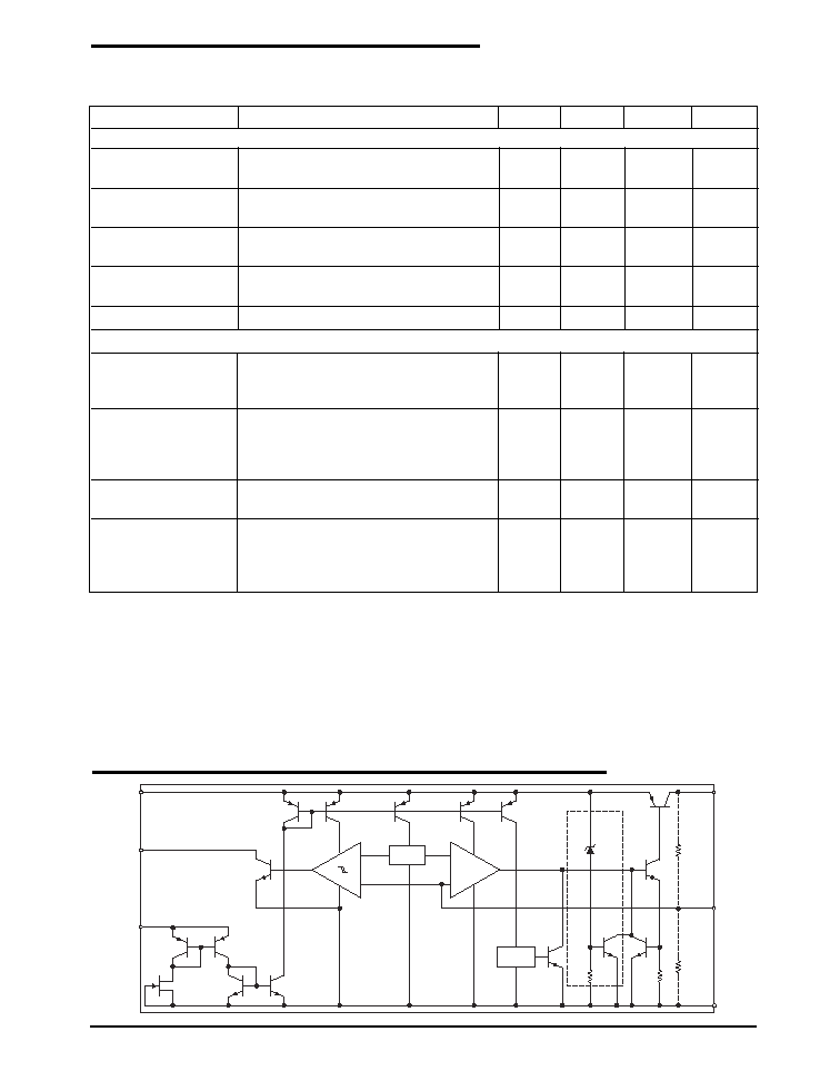
Reference
Thermal
Shutdown
EN
IN
OUT
ADJ
GND
O.V
I
LIMIT
28V
R1*
R2*
1.180V
1.240V
+
+
-
-
FLAG
BLOCK DIAGRAM
ELECTRICAL CHARACTERISTICS
Date:5/25/04
SP29150/51/52/53 1.5A Low Dropout Voltage Regulator
© Copyright 2004 Sipex Corporation
4
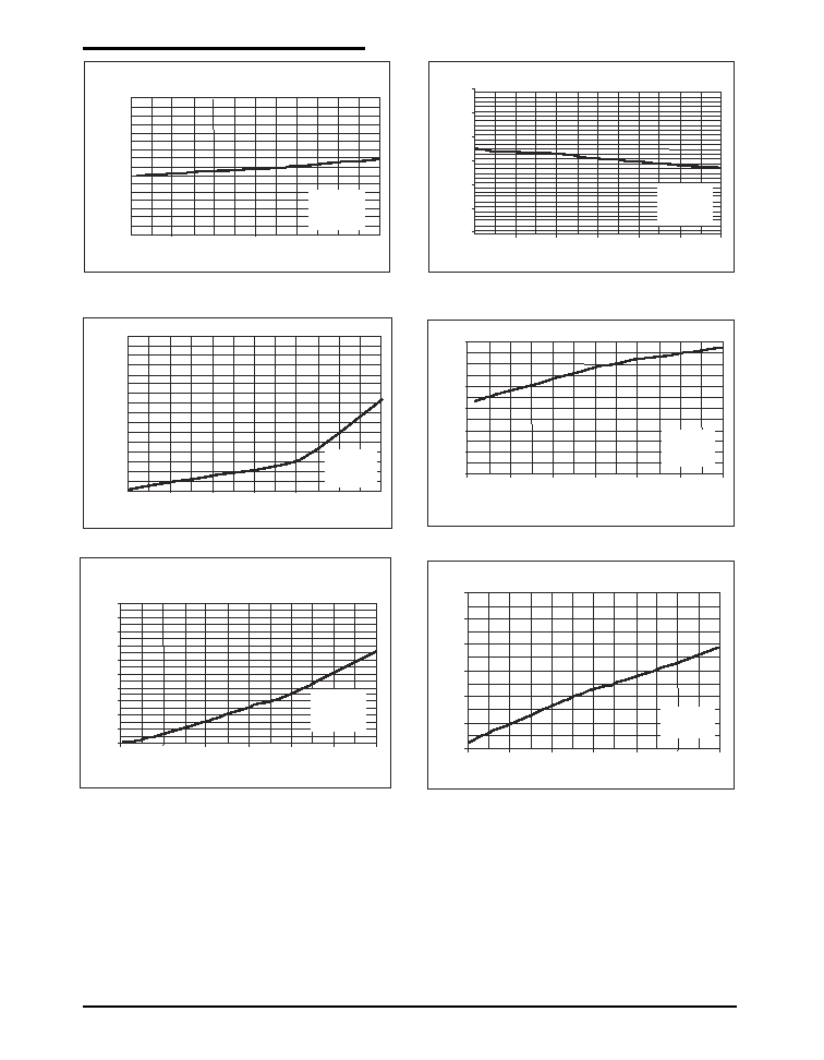
TYPICAL PERFORMANCE CHARACTERISTICS
Figure 3. Line Regulation
Figure 4. Load Regulation
Figure 5. Ground Current vs Load Current
Figure 6. Ground Current vs Input Voltage
Figure 7. Ground Current vs Load Current in Dropout
Figure 8. Dropout Voltage vs Load Current
3.280
3.285
3.290
3.295
3.300
3.305
3.310
3.315
3.320
4
6
8
10
12
14
16
Vin (V)
3.3V Device
IL = 10mA
CL = 10 F
Vout (V)
3.280
3.285
3.290
3.295
3.300
3.305
3.310
0
0.25
0.5
0.75
1
1.25
1.5
IL (A)
Vin = 4.3V
CL = 10 F
3.3V Device
Vout (V )
0.0
10.0
20.0
30.0
40.0
50.0
60.0
70.0
80.0
0
0.25
0.5
0.75
1
1.25
1.5
IL (A)
3.3V Device
Vin = 4.3V
CL = 10 F
Ignd (mA)
180
200
220
240
260
280
300
4
6
8
10
12
14
16
Vin (V)
3.3V Device
IL = 10mA
CL = 10 F
Ignd (uA)
0
10
20
30
40
50
60
70
80
90
100
0
0.25
0.5
0.75
1
1.25
1.5
IL (A)
3.3V Device
Vin = 3.2V
CL = 10 F
Ignd (mA)
0
100
200
300
400
500
600
0
0.25
0.5
0.75
1
1.25
1.5
IL (A)
3.3V Device
CL = 10 F
Vdropout (mV)

5
Date:5/25/04
SP29150/51/52/53 1.5A Low Dropout Voltage Regulator
© Copyright 2004 Sipex Corporation
Figure 9. Ground Current vs Temperature
Figure 10. Output Voltage vs Temperature at
at I
LOAD
=10mA
I
LOAD
=10mA
Figure 11. Ground Current vs Temperature at
Figure 12. Output Voltage vs Temperature in Dropout
I
LOAD
=500
at I
LOAD
=750mA
Figure 13. Ground Current vs Temperature at
Figure 14. Output Current vs Temperature in Dropout
I
LOAD
=1.5A
at I
LOAD
=1.5A
TYPICAL PERFORMANCE CHARACTERISTICS
180
190
200
210
220
230
240
250
260
270
280
-40
-20
0
20
40
60
80
100
120
Temperature (
o
C)
3.3V Device
Vin = 4.3V
IL = 10mA
CL = 10 F
Ignd (uA)
5.00
5.20
5.40
5.60
5.80
6.00
6.20
6.40
6.60
6.80
7.00
-40
-20
0
20
40
60
80
100
120
Temperature (
o
C)
3.3V Device
Vin = 4.3V
IL = 500mA
CL = 10 F
Ignd (mA)
20
21
22
23
24
25
26
27
28
29
30
-40
-20
0
20
40
60
80
100
120
Temperature (
o
C)
3.3V Device
Vin = 3.2V
IL = 750mA
CL = 10 F
Ignd (mA)
36.0
38.0
40.0
42.0
44.0
46.0
48.0
50.0
52.0
-40
-20
0
20
40
60
80
100
120
Temperature (
o
C)
3.3V Device
Vin = 4.3V
IL = 1.5A
CL = 10 uF
Ignd (mA)
70
75
80
85
90
95
100
-40
-20
0
20
40
60
80
100
120
Temperature (
o
C)
3.3V Device
Vin = 3.2V
IL = 1.5A
CL = 10 F
Ignd (mA)
3.220
3.230
3.240
3.250
3.260
3.270
3.280
3.290
3.300
3.310
3.320
-40
-20
0
20
40
60
80
100
120
Temperature (
o
C)
3.3V Device
Vin = 4.3V
IL = 10mA
CL = 10 F
Vout